
Zhaosong Li, Dan Lu, Yiming He, Fangyuan Meng, Xuliang Zhou, Jiaoqing Pan, "InP-based directly modulated monolithic integrated few-mode transmitter," Photonics Res. 6, 463 (2018)
- Photonics Research
- Vol. 6, Issue 5, 463 (2018)
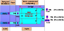
Fig. 1. Diagram of the few-mode transmitter. DML, directly modulated laser. MMI, multimode interference coupler. W is the width of the MMI section. L π W 1 and W 2 are the widths of Port4 and Port3, respectively.
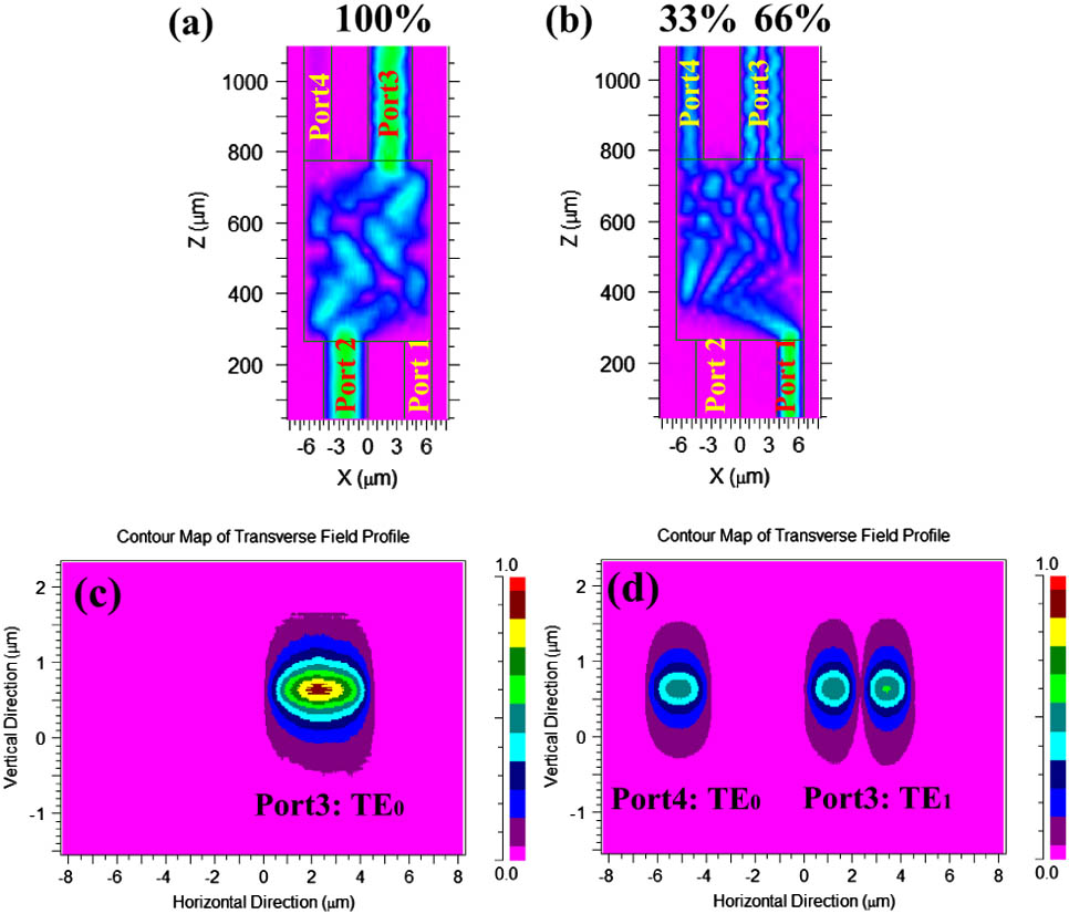
Fig. 2. Optical fields of the MMI-based mode converter/multiplexer. (a), (b) in the X - Z X - Y
Fig. 3. Epitaxial structure of the few-mode transmitter. SCH, separate confinement heterostructure; QW, quantum well; QB, quantum barrier.
Fig. 4. PL spectrum of the material. The PL wavelength for the passive and active sections were around 1.2 and 1.55 μm, respectively.
Fig. 5. SEM pictures of (a) the butt-joint interface and (b) MQWs, and (c) the microscope picture of the transmitter.
Fig. 6. Near-field pattern of (a) TE 0 TE 1 LP 01 LP 11
Fig. 7. PIV curve, spectrum, and frequency response characteristic of DML1 (TE 1 − 3 dB
Fig. 8. PIV curve, spectrum and frequency response characteristic of DML2 (TE 0 − 3 dB
Fig. 9. 10 Gbit/s eye diagram of the (a) TE 0 TE 1
Fig. 10. BER curves at 10 Gbit/s for the TE 0 TE 1


Set citation alerts for the article
Please enter your email address

© Copyright 2018-2021 | Chinese Laser Press. All Rights Reserved 沪ICP备15018463号-20