Abstract
A monolithic integrated few-mode transmitter comprising of two directly modulated distributed feedback lasers and a multimode-interference-coupler-based mode converter-multiplexer with 66% mode conversion efficiency was designed and demonstrated. A fundamental mode and a first-order mode were successfully generated from the transmitter, with the output power of 4 and 5.5 mW at a pump current of around 150 mA, respectively, at the common output port. The small signal modulation bandwidth of the and channels reached 17.4 and 14.7 GHz, respectively. Error-free direct modulation of the two-mode transmitter was demonstrated, with a power penalty of 4.3 dB between the mode and the mode at the bit error rate of .1. INTRODUCTION
With the development of communication technology, the ever-increasing demands for bandwidth and transmission capacity are pushing device speed and traditional multiplexing technology close to their limits. In recent years, mode division multiplexing (MDM) has been proposed to further increase the transmission capacity of communication networks or on-chip systems [1–9]. In a typical MDM system, high-order modes are converted from a single-mode laser source, then externally modulated and multiplexed into a few-mode channel. The laser sources, modulators, mode converters, and multiplexers are usually discrete devices, resulting in a complex and bulky transmitter system [10–12]. Much effort has been put into the design and development of integrated MDM devices. Various on-chip mode converters and mode (de)multiplexers have been reported either in the silicon [13–15] or the InP platforms [5,7,16,17], aiming at not only long-haul optical fiber communication systems but also short-reach optical interconnects. Up to now, most on-chip MDM devices are passive, performing the mode-manipulation functions. It would be more attractive if all the functional components were integrated into a single chip, forming a standalone few-mode transmitter. The silicon platform is a popular choice for passive devices due to its more standardized design, lower loss, and accurate processing control [1]. But the difficulty in efficient lasing and amplification in the silicon platform remains as a problem for a fully integrated few-mode transmitter, while the InP platform, with the advantage in the active and passive integration, offers a full integration possibility to bring together the functionality of lasers, modulators, and mode-manipulation devices. It is a promising solution to considerably reduce the complexity, footprint, power consumption, and cost of an MDM system.
In this paper, we report, to the best of our knowledge, the first directly modulated monolithic integrated few-mode transmitter in the InP platform. Two directly modulated lasers (DML) and a mode converter-multiplexer with mode conversion () efficiency of 66% were integrated in a single chip. A fundamental mode and a first-order mode with output power of 4 and 5.5 mW, respectively, at a pump current around 150 mA were generated from the few-mode transmitter. and modes were successfully excited by the two TE modes. The small signal bandwidth of the two DMLs reached 17.4 and 14.7 GHz, respectively. Error-free direct modulation was demonstrated, with a power penalty of 4.3 dB between the mode and the mode at the bit error rate of .
2. PRINCIPLE AND FABRICATION
Figure 1 shows a diagram of the few-mode transmitter. It consists of two DMLs as light sources and modulators and a multimode interference coupler (MMI) [16–19] as the mode converter/multiplexer. DML1 and DML2 are distributed feedback (DFB) lasers, responsible for generating two directly modulated modes. The principle of the MMI-based mode converter/multiplexer can be referred to Refs. [20–22]. By properly choosing the position and width of the input and output ports of the MMI, mode conversion and multiplexing with different mode conversion efficiency can be realized [20]. In this work, an MMI with 66% mode conversion efficiency () is adopted. The length of the multimode section of the MMI is , where is the beat length of the two lowest-order modes. As shown in Fig. 1, the input Port1 and Port2 are placed, respectively, at the bottom and W/3 from the top, where W is the real MMI width. Port3 and Port4 are placed at W/3 from the bottom and the top, respectively. Port3 is the output port for the multiplexed modes, comprising the mode generated from DML2 and mode converted from DML1.
Sign up for Photonics Research TOC. Get the latest issue of Photonics Research delivered right to you!Sign up now
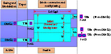
Figure 1.Diagram of the few-mode transmitter. DML, directly modulated laser. MMI, multimode interference coupler. W is the width of the MMI section. is the beat length of the two lowest-order modes. W1 and W2 are the widths of Port4 and Port3, respectively.
The MMI-based mode converter/multiplexer was first simulated by the 3D beam propagation method before fabrication. The optimum width and length of the MMI section were found to be 13 and 500 μm, respectively. In the simulation, the operation wavelength was 1550 nm. The material refractive indices of the InP buffer layer, the core layer, i.e., the InGaAsP with 1.2 μm bandgap (1.2Q), and the cladding (InP) were set to be 3.167, 3.382, and 3.167, respectively. The widths of the Port1, 4 and Port2, 3 were 2.7 and 4.5 μm, respectively. The DMLs were ridge DFB lasers with a ridge width of 3 μm and length of 250 μm, respectively. The holographic exposure technology was used in the grating fabrication, and the grating period was 240 nm. High-frequency electrodes were adopted in the design. A taper structure was placed between DML2 and Port2 to provide an adiabatic transition between the two ridges with different widths. To eliminate the influence of the output at Port4, a curved waveguide was adopted to guide the unused mode power off the testing path. The total size of the transmitter was about .
As shown in Fig. 2, the fundamental mode from Port2 will emit from Port3 with the mode pattern unchanged after passing through the MMI, while the fundamental mode from Port1 will be converted into the first-order mode and emit from Port3. The optical fields in the plane and the plane of the MMI-based mode converter/multiplexer are shown in Figs. 2(a), 2(b) and 2(c), 2(d), respectively.

Figure 2.Optical fields of the MMI-based mode converter/multiplexer. (a), (b) in the plane and (c), (d) in the plane.
Figure 3 shows the epitaxial structure of the few-mode transmitter. The active section consists of a 0.5 μm InP buffer, an 80 nm 1.2Q lower separate confinement heterostructure (SCH) layer, multiple quantum wells (MQWs), an 80 nm 1.2Q upper SCH layer, a 1.7 μm InP cladding, and a 0.2 μm InGaAs contact layer. The structure of the MMI section consists of a 0.5 μm InP buffer, a 0.3 μm core layer with 1.2Q and a 1.7 μm InP cladding. The material structures were grown by metal organic chemical vapor deposition in a three-step regrowth progress. Butt-joint technology was used to integrate the DFB-LDs with the MMI-based mode converter/multiplexer. The photoluminescence (PL) spectrum of the active section and passive section is shown in Fig. 4. The PL wavelengths for the passive and active sections were around 1.2 and 1.55 μm, respectively. The ridge waveguide was about 1.9 μm in height. The scanning electron microscope (SEM) pictures of the butt-joint interface and MQWs and the microscope picture of the transmitter are shown in Fig. 5.
Figure 3.Epitaxial structure of the few-mode transmitter. SCH, separate confinement heterostructure; QW, quantum well; QB, quantum barrier.
Figure 4.PL spectrum of the material. The PL wavelength for the passive and active sections were around 1.2 and 1.55 μm, respectively.
Figure 5.SEM pictures of (a) the butt-joint interface and (b) MQWs, and (c) the microscope picture of the transmitter.
3. DEVICE CHARACTERIZATION
The chip was tested on an AlN submount with a controlled temperature of 20°C. The mode pattern of the transmitter was first evaluated. Figures 6(a) and 6(b) demonstrate the near-field pattern of the fundamental mode and the first-order mode at the output Port3, respectively, corresponding to the separate operation of DML2 and DML1. The generated two modes were then coupled into a 200 m two-mode few mode fiber to excite the fiber modes. Figures 6(c) and 6(d) show the and modes excited by the and modes, respectively. A clear optical fiber mode pattern can be excited by the few-mode transmitter.
Figure 6.Near-field pattern of (a) mode and (b) mode measured at the common output Port3 of the transmitter, and the excited (c) mode and (d) mode measured from a 200 m two-mode fiber, respectively.
The light power and voltage versus injection current (PIV) curve, spectrum and the small signal modulation bandwidth of DML1 and DML2 are shown in Figs. 7 and 8, respectively. The threshold currents of the two DMLs were 25 and 30 mA, respectively, as shown in Figs. 7(a) and 8(a). The optical powers of the DML1 and DML2 were 9 and 17.5 mW at around 150 mA, respectively. The optical powers measured at Port3 were 4 and 5.5 mW, respectively, as shown in the blue curves in Figs. 7(a) and 8(a). The mode conversion efficiency from mode to mode was about 60%, which was consistent with our design. While the mode power originated from DML2 was considerably low, it could be due to the processing problem at the taper structure interfaces. The kinks in the PI curves correspond to the mode hopping points, which should come from the influence of the facet or MMI interface reflections of the waveguide. The mode hopping may result in a different lasing wavelength, change of optical power, and eye diagram degradation. The reflection can be avoided by introducing antireflecting coating at the facet and tapered structure at the MMI interface. The wavelength of the two DMLs was around 1538 nm, as shown in Figs. 7(b) and 8(b). In single-mode state, the side mode suppression ratios for both DMLs were above 35 dB. The small-signal modulation bandwidth of the two DMLs was 14.7 GHz and 17.4 GHz at bias currents of 49 and 64 mA, respectively, measured by a vector network analyzer (VNA, HP 8510C). The differences in wavelength, power, and modulation bandwidth between the two DMLs could be due to the processing errors in grating and waveguide etching, etc.
Figure 7.PIV curve, spectrum, and frequency response characteristic of DML1 ( channel). (a) PIV curve, (b) optical spectrum, (c) bandwidth.
Figure 8.PIV curve, spectrum and frequency response characteristic of DML2 ( channel). (a) PIV curve, (b) optical spectrum, (c) bandwidth.
Then, the DMLs were modulated, separately, at a bit rate of 10 Gbit/s using a bit error rate (BER) tester (Agilent Technologies N4901B). The eye diagrams measured at Port3 are shown in Fig. 9. Figures 9(a) and 9(b) are the eye diagrams of the fundamental mode and first-order mode. The bias currents of DML1 and DML2 were 66 and 109 mA at driving voltages of 1.66 and 1.7 V, respectively. Error-free performance of the two mode channels can be obtained for back-to-back BER test. The back-to-back BER curves are shown in Fig. 10. The power penalty between mode and mode is 4.3 dB at the BER of .
Figure 9.10 Gbit/s eye diagram of the (a) mode channel and (b) mode channel.
Figure 10.BER curves at 10 Gbit/s for the mode channel and mode channel.
4. SUMMARY
An InP-based monolithically integrated few-mode transmitter is demonstrated. and modes were generated from the transmitter, and then the two modes were used to excite the and fiber modes. The small-signal bandwidths for the two mode channels reached 17.4 and 14.7 GHz, respectively. A clear, opened 10 Gbit/s eye diagram was obtained. The BER performance of the few-mode transmitter was evaluated. The directly modulated monolithic integrated few-mode transmitter may find potential applications in short-range or on-chip MDM systems, where intensity modulation with direct detection (IM/DD) is preferred.
References
[1] D. Chen, X. Xiao, L. Wang, Y. Yu, W. Liu, Q. Yang. Low-loss and fabrication tolerant silicon mode-order converters based on novel compact tapers. Opt. Express, 23, 11152-11159(2015).
[2] W. Zhao, K. Chen, J. Wu, K. Chiang. Horizontal directional coupler formed with waveguides of different heights for mode-division multiplexing. IEEE Photon. J., 9, 6601509(2017).
[3] K. Chen, Z. Nong, J. Zhang, X. Cai, S. He, L. Liu. Multimode 3 dB coupler based on symmetrically coupled waveguides for on-chip mode division multiplexing. J. Lightwave Technol., 35, 4260-4267(2017).
[4] X. Wu, K. Xu, C. Huang, C. Shu, H. Tsang. Mode division multiplexed 3 × 28 Gbit/s on-chip photonic interconnects. Conference on Lasers and Electro-Optics (CLEO), STu4G.6(2016).
[5] Z. Li, D. Lu, L. Zhao, S. Liang, X. Zhou, J. Pan. An InP-based two-mode converter-(de)multiplexer with 100% mode conversion efficiency by using multimode interference couplers as the building blocks. Conference on Lasers and Electro-Optics (CLEO), JW2A.123(2016).
[6] Y. Chaen, R. Tanaka, K. Hamamoto. Optical mode converter using multi-mode interference structure. Microoptics Conference (MOC), 1-2(2013).
[7] L. Zhang, D. Lu, Z. Li, B. Pan, L. Zhao. C-band fundamental/first-order mode converter based on multimode interference coupler on InP substrate. J. Semicond., 37, 124005(2016).
[8] D. Dai, J. Wang, Y. Shi. Silicon mode (de)multiplexer enabling high capacity photonic networks-on-chip with a single-wavelength-carrier light. Opt. Lett., 38, 1422-1424(2013).
[9] D. Dai, J. Wang, S. He. Silicon multimode photonic integrated devices for on-chip mode-division-multiplexed optical interconnects. Prog. Electromagn. Res., 143, 773-819(2013).
[10] S. Cai, S. Yu, M. Lan, L. Gao, S. Nie, W. Gu. Broadband mode converter based on photonic crystal fiber. IEEE Photon. Technol. Lett., 27, 474-477(2015).
[11] F. Ferreira, D. Borne, P. Monteiro, H. Silva. Crosstalk optimization of phase masks for mode multiplexing in few mode fibers. Optical Fiber Conference (OFC), JW2A.37(2012).
[12] M. Segall, V. Rotar, J. Lumeau, L. Glebov. Volume phase plates for optical beam control. Frontiers in Optics, JWA02(2010).
[13] D. Dai, M. Mao. Mode converter based on an inverse taper for multimode silicon nanophotonic integrated circuits. Opt. Express, 23, 28376-28388(2015).
[14] J. Xing, Z. Li, X. Xiao, J. Yu, Y. Yu. Two-mode multiplexer and demultiplexer based on adiabatic couplers. Opt. Lett., 38, 3468-3470(2013).
[15] L. Han, S. Liang, H. Zhu, L. Qiao, J. Xu, W. Wang. Two-mode de/multiplexer based on multimode interference couplers with a tilted joint as phase shifter. Opt. Lett., 40, 518-521(2015).
[16] F. Guo, D. Lu, R. Zhang, H. Wang, C. Ji. A two-mode (de)multiplexer based on multimode interferometer coupler and Y-junction on InP substrate. IEEE Photon. J., 8, 2700608(2016).
[17] Z. Li, D. Lu, B. Zuo, S. Liang, X. Zhou, J. Pan. Proposal of an InP-based few-mode transmitter based on multimode interference couplers for wavelength division multiplexing and mode division multiplexing applications. Chin. Opt. Lett., 14, 080601(2016).
[18] M. Bachmann, P. A. Besse, H. Melchior. General self-imaging properties in N × N multimode interference couplers including phase relations. Appl. Opt., 33, 3905-3911(1994).
[19] M. Bachmann, P. A. Besse, H. Melchior. Overlapping-image multimode interference couplers with a reduced number of self-images for uniform and nonuniform power splitting. Appl. Opt., 34, 6898-6910(1995).
[20] J. Leuthold, J. Eckner, E. Gamper, P. A. Besse, H. Melchior. Multimode interference couplers for the conversion and combining of zero- and first-order modes. J. Lightwave Technol., 16, 1228-1239(1998).
[21] G. Fei, D. Lu, R. Zhang, H. Wang, W. Wang, C. Ji. Two-mode converters at 1.3 μm based on multimode interference couplers on InP substrates. Chin. Phys. Lett., 33, 024203(2016).
[22] Z. Li, D. Lu, S. Liang, Z. Liu, J. Pian. A monolithically integrated InP-based few-mode laser. Asia Communications and Photonics Conference (ACP), AF3B.6(2016).


