Jin Sung Kang, Ju-An Yoon, Seung Il Yoo, Jin Wook Kim, Bo Mi Lee, Hyeong Hwa Yu, C.-B. Moon, Woo Young Kim. Highly efficient blue organic light-emitting diodes using various hole and electron confinement layers[J]. Chinese Optics Letters, 2015, 13(3): 032301
Copy Citation Text
In this Letter, blue phosphorescence organic light-emitting diodes (PHOLEDs) employ structures for electron and/or hole confinement; 1,3,5-tris(N-phenylbenzimiazole-2-yl)benzene is used as a hole confinement layer and tris-(phenylpyrazole)iridium [] is utilized for an electron confinement layer (ECL). The electrical and optical properties of the fabricated blue PHOLEDs with various carrier-confinement structures are analyzed. Structures with a large energy offset between the carrier confinement and emitting layers enhance the charge-carrier balance in the emitting region, resulting from the effective carrier confinement. The maximum external quantum efficiency of the blue PHOLEDs with the double-ECLs is 24.02% at and its luminous efficiency is , which is 70.47% improved compared to the device without a carrier-confinement layer.
Organic light-emitting diodes (OLEDs) have heralded a new era in chemistry and physics since the multi-layered OLED was reported in 1987[1]; OLEDs have been used as flat-panel displays and in solid-state lighting applications[2,3]. Although there has been great progress on phosphorescence OLEDs (PHOLEDs)[4–6], the efficiency of blue PHOLEDs requires improvement for commercialization[4,6,7]. Various methods have been reported to improve device performance[8–14] since PHOLEDs were discovered[15–17]. Above all, efficient charge-carrier injection and exciton confinement in the emitting layers (EMLs) have been considered as key factors to obtain high-performance blue OLEDs[14–19]. In fact, quantum well structures leading to carrier confinement have been proven to achieve better device performance such as a high luminous efficiency[20–23], a tunable electroluminescence (EL) zone[24], and carrier balance[25–28], resulting in enhanced exciton yield in the emitting region[22].
In this Letter, carrier-confinement layers were introduced in the EML to enhance the charge balance of OLED devices. For highly efficient blue PHOLEDs the following key points should be considered: (1) use of charge transport layers with a high triplet energy state to block triplet exciton quenching, (2) realizing effective carrier transport to EMLs with a high carrier transport property and favorable highest occupied molecular orbital (HOMO)/lowest unoccupied molecular orbital (LUMO) energy level with neighboring layers, and (3) utilizing electron- and hole-confinement structures.
Among these factors we employ the concept of the carrier-confinement structures to optimize device performance. We also vary the combinations of the EML and carrier-confinement layers to understand the effect of the electron and/or hole confinement in the EML region.
Sign up for Chinese Optics Letters TOC. Get the latest issue of Chinese Optics Letters delivered right to you!Sign up now
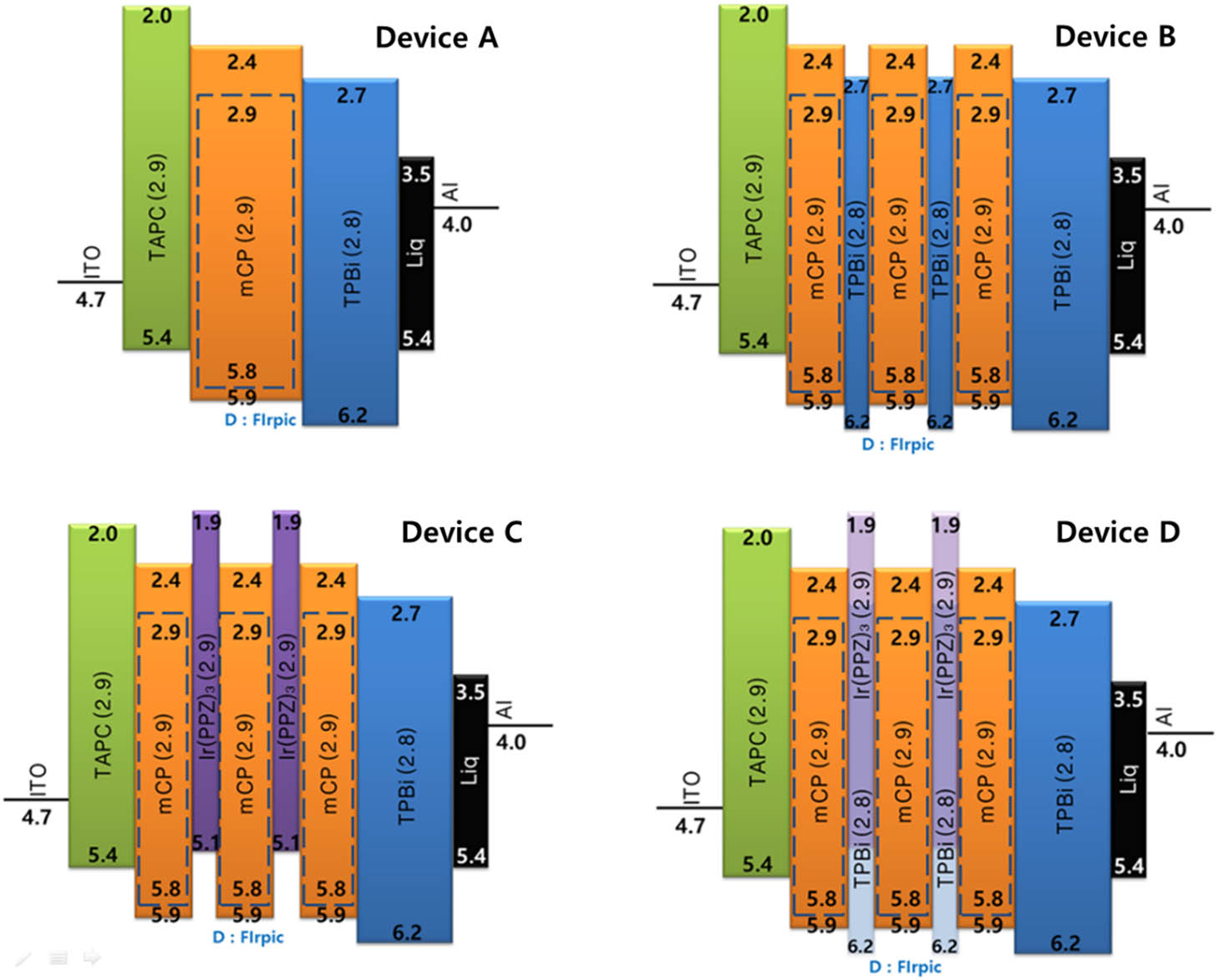
External quantum efficiency (EQE) and Intensity–Voltage–Luminance (I–V–L) characteristics were observed to investigate the effect of the carrier-confinement layer structures. Figure 1 shows the energy band diagrams of blue PHOLED devices. Device A was a reference device, Device B has a hole-confiment layer (HCL), Device C has an electron-confinement layer (ECL), and Device D has a HCL and ECL (). The use of 1,3,5-tris(N-phenylbenzimiazole-2-yl)benzene (TPBi) as the ETL and HCL provides simplicity for the device fabrication process.
Figure 1.Energy band diagrams of blue PHOLED devices.
Glass substrates [coated with indium tin oxide (ITO)] with a sheet resistance of were used. The ITO glass was cleaned in an ultrasonic bath by a regular cleaning sequence: deionized water, isopropyl alcohol, acetone, deionized water, and isopropyl alcohol. Thereafter, the pre-cleaned ITO glass was treated with plasma under vacuum conditions of , 100 W, for 2 min. All organic materials were deposited by thermal evaporation under a pressure of . The blue PHOLEDs were composed of 4,4′-cyclohexylidenebis [N,N-bis(4-methylphenyl)benzenamine] (TAPC) as a hole transport layer (HTL), EML, carrier confiment layers, TPBi as an ETL, 8-hydroxyquinolinolato-lithium (Liq) as an electron injection layer (EIL), and aluminum as a cathode. 1,3-bis(N-carbazolyl) benzene (mCP) is doped with bis[2-(4,6-difluorophenyl)pyridinato-,N](picolinato)iridium(III) (FIrpic) for the EML, and TPBi and are employed as the HCL and ECL, respectively. The thickness of the individual EML was optimized; however, the total thickness of the emitting region was kept at 30 nm. The electrical and optical characteristics of the blue PHOLEDs were measured and analyzed by a Keithley 238, LMS PR-650 spectrophotometer, colorimeter, and the I–V–L system.
Figure 2 shows the current density–voltage characteristics of Devices A–D. The characteristics of the current density are attributed to the carrier mobility and the energy barrier height for injection. The current densities of Devices A–D at 10 V were 88.93, 74.19, 49.05, and , respectively. The conventional OLED with no confinement layer, Device A, has the highest current density because in other devices, the carrier flow is lowered by the large existing energy barriers between the EML and carrier-confinement layers. This phenomenon can be explained by the Schottky diode equation describing the relation of I–V characteristics as follows where is a constant factor of the OLED, is the quantity of electric charge, is the barrier height, is the Boltzmann constant, is the temperature, and is the applied voltage. From Eq. (1) it was found that the barrier height () explains why Devices B, C, and D show lower current density than Device A. In particular the lower current density from Devices C and D is attributable to the larger energy offset in the LUMO side compared to Device A[29].
Figure 2.Current density–voltage characteristics of blue PHOLEDs.
The luminance as a function of density of Devices A–D is shown in Fig. 3(a). Luminance of Devices A–D were 20240, 21890, 29430, and , respectively, at . In general, the mobility of holes is faster than that of electrons[30,31]. Hole mobility of TAPC is whereas electron mobility of TPBi is . The effective electron confinement in the EML leads to a high local electron density which results in an improved charge-carrier balance. Although both Devices C and D used ECLs, the luminance of Device C is higher than Device D because the carrier-confinement layers of Device D are composed of a mixture of TPBi (the HCL) and (the ECL), providing additional available electron or hole transport channels so that less carrier confinement was created. As shown in Fig. 3(b) the normalized EL spectra show that all the devices are nearly identical. This phenomenon elucidates that varying the confinement layer affects the energy transfer between neither the host nor dopant in an EML, nor in the recombination zone.
Figure 3.(a) Luminance–current density characteristics of blue PHOLEDs; (b) EL spectra of blue PHOLEDs at a bias of 6 V.
Therefore, it was observed that the luminance is affected by the carrier confinement structure and Device C has an ideal EML structure for efficient electron and hole recombination.
Figure 4 shows the luminous efficiency–luminance and power efficiency–luminance characteristics of the blue PHOLEDs. The maximum luminous efficiencies of Devices A–D were 25.67, 28.52, 43.76, and , respectively. Device C has the highest luminous efficiency whereas the lowest luminous efficiency was found from Device A. Usually hole density is higher than electron density in an EML because a hole has a faster mobility than an electron. However, Device B with the HCL performs more recombinations in an EML due to its higher hole density yet does not show a significant improvement in the luminious efficiency because the electron density is used to influence more than the hole density in hole-electron recombinations.
Figure 4.(a) Luminous efficiency–luminance characteristics and; (b) power efficiency–luminance characteristics of blue PHOLEDs.
Despite the lower mobility of electrons, in general, compared to that of holes in organic layers, well-balanced charge carriers can be obtained by the carrier confinement in the emitting region due to the large energy barriers between the EML and carrier-confinement layers, bringing a higher probability of electron and hole recombination. Also, hole traps occur due to the low HOMO energy level of , which causes an efficient charge-carrier balance and enhanced recombination. As seen in Fig. 4(a), the highest luminous efficiency was achieved from Device C with only ECLs and Device D with both the ECL and HCL shows the second-highest luminous efficiency. The structure with only ECLs gives a stronger impact on the luminous efficiency of the devices.
The external quantum efficiency () of OLEDs can be explained as the ratio of the number of photons emitted from the OLEDs to that of injected hole and electrons into the organic layers, and is described with four different factors as follows where the charge balance factor accounts for the probability of electron and hole recombination, and the singlet-triplet factor, , distinguishes between the two material classes of the fluorescent and phosphorescent emitters. The fluorescent emitters can assume and for the phosphorescent emitters . The third factor represents the radiative quantum efficiency of the emitting material in an unbounded medium. The outcoupling factor describes efficiency of light extraction from the devices[29,32,33].
Figure 5 plots external quantum efficiency as a function of luminance for Devices A–D. The external quantum efficiencies of Devices A–D were 14.78%, 16.26%, 24.02%, and 22.05%, respectively, at . Device C has the highest external quantum efficiency while Device A has lowest external quantum efficiency.
Figure 5.External quantum efficiency–luminance characteristics of blue PHOLEDs.
Considering that the four factors of the external quantum efficiency of Devices A–D correspond to the same emitting materials yet different layer configurations (depending on the use of electron and/or hole confinement layers), , , and of each device are the almost the same value, except for . From this aspect, the highest external quantum efficiency from Device C with the double-ECLs can be explained with a higher value of , resulting from the high local electron density. In addition, the absence of the carrier confinement layers in Device A causes relatively imbalanced charge-carriers in the emitting zone, showing the lowest external quantum efficiency among the four devices.
In conclusion, we demonstrate highly efficient blue PHOLEDs with the carrier-confinement layers contributing to improved charge-carrier balance in the emitting region. It is observed that the device with the ECL shows higher efficiency compared to the device with the HCL. In particular, Device C with double-ECLs has with the 70.47% improvement in comparison to Device A with the absence of the carrier-confinement layers, and 23.40% maximum external quantum efficiency is achieved. We will continue research on understanding and optimizing the effects of hole and electron confinement in the emitting area to achieve an enhanced luminous efficiency of blue PHOLEDs.
References
[1] C. W. Tang, S. A. VanSlyke. J. Appl. Phys., 51, 21(1987).
Jin Sung Kang, Ju-An Yoon, Seung Il Yoo, Jin Wook Kim, Bo Mi Lee, Hyeong Hwa Yu, C.-B. Moon, Woo Young Kim. Highly efficient blue organic light-emitting diodes using various hole and electron confinement layers[J]. Chinese Optics Letters, 2015, 13(3): 032301