1Interdisciplinary Center for Quantum Information, New Cornerstone Science Laboratory, State Key Laboratory of Extreme Photonics and Instrumentation, College of Optical Science and Engineering, Zhejiang University, Hangzhou, China
2Jiaxing Key Laboratory of Photonic Sensing & Intelligent Imaging, Intelligent Optics & Photonics Research Center, Jiaxing Research Institute Zhejiang University, Jiaxing, China
3Collaborative Innovation Center of Extreme Optics, Shanxi University, Taiyuan, China
An optical micro/nanofiber (MNF) is a quasi-one-dimensional free-standing optical waveguide with a diameter close to or less than the vacuum wavelength of light. Combining the tiny geometry with high-refractive-index contrast between the core and the surrounding, the MNF exhibits favorable optical properties such as tight optical confinement, strong evanescent field, and large-diameter-dependent waveguide dispersion. Meanwhile, as a quasi-one-dimensional structure with extraordinarily high geometric and structural uniformity, the MNF also has low optical loss and high mechanical strength, making it favorable for manipulating light on the micro/nanoscale with high flexibility. Over the past two decades, optical MNFs, typically being operated in single mode, have been emerging as a miniaturized fiber-optic platform for both scientific research and technological applications. In this paper, we aim to provide a comprehensive overview of the representative advances in optical MNFs in recent years. Starting from the basic structures and fabrication techniques of the optical MNFs, we highlight linear and nonlinear optical and mechanical properties of the MNFs. Then, we introduce typical applications of optical MNFs from near-field optics, passive optical components, optical sensors, and optomechanics to fiber lasers and atom optics. Finally, we give a brief summary of the current status of MNF optics and technology, and provide an outlook into future challenges and opportunities.
An optical micro/nanofiber (MNF) is a kind of quasi one-dimensional (1D) free-standing optical waveguide with a diameter close to or less than the vacuum wavelength of the transmitted light. The earliest report of glass MNFs with diameters around 1 µm could be traced back to 1887 when Boys fabricated glass threads by drawing molten minerals at a high speed[1]. However, at that time, those MNFs were not used for optical waveguiding. Instead, owing to their excellent elasticity and small resilience of these threads, they were used as elastic springs or suspension wire for measuring a very small force or torsion[2,3]. In 1910, Hondros and Debye reported the first theoretical model for waveguiding light along a dielectric cylinder, and showed that electromagnetic waves could be confined and propagated in a lossless dielectric cylindrical waveguide, with a diameter below the wavelength[4]. However, it was not until the 1950s that these waveguiding modes in cylindrical waveguides, named as “surface waves,” began to receive much attention[5–8]. In 1951, O’Brien and van Heel proposed covering low-index cladding on the surface of cylindrical waveguides to reduce the crosstalk between the waveguides[9], and in the following years, Hopkins and Kapany demonstrated sub-micrometer multiple fibers coated with low-index cladding for image transmission[10–12]. In 1966, Kao and Hockham proposed the possibility of developing low-loss glass fibers[13], opening up the era of optical fiber communication, as well as low-loss fiber optics and technology. From then on, taper drawing a standard silica fiber became a routine approach to fabricating an MNF (typically called the fiber taper) connected with a silica fiber through a conical taper, and the shape of the taper and the diameter of the waist (i.e., MNF) could be controlled much better than before[14–18]. Relying on the surface waves (i.e., waveguided evanescent fields) of these MNFs[19,20], a variety of applications were proposed or developed including optical filters[21,22], couplers[23,24], evanescent field amplification[25], sensors[26,27], and supercontinuum generation[28], while the diameters of the MNFs used or assumed were mostly larger than the vacuum wavelength of the guided light.
In 2003, Tong and Mazur experimentally demonstrated that subwavelength-diameter silica nanofibers taper drawn from silica fibers could be used for low-loss optical waveguiding[29], opening an opportunity for guiding light in MNFs with smaller sizes and stronger “surface waves,” which in turn, bestowed the MNFs with tight optical confinement, strong evanescent fields, and highly engineerable waveguide dispersion[30]. Shortly after, such MNFs were experimentally proved to have losses (e.g., 1.4 dB/mm[31]) lower than all other subwavelength-width optical waveguides in visible and near-infrared (NIR) spectral ranges[32]. Since then, a number of improved MNF fabrication techniques, based on flame-heated[33–40], electrically heated[41–45], and laser-heated[46–48] taper drawings of standard optical fibers, have been demonstrated[49,50]. So far, waveguiding loss of silica MNFs can typically be below 0.1 dB/m, with the lowest value of 0.03 dB/m[37] (i.e., three orders of magnitude lower than that of a planar waveguide with similar width[51]). Also, with a high-precision real-time diameter-monitoring technique[38,39,45,50,52], the diameter of the MNF can be obtained on-demand, with the best precision of [39]. Moreover, by keeping the tapering angle below the mode-transition critical angle, the single-mode light field in a standard-sized fiber can be squeezed into an MNF mode almost losslessly (typical loss ), with the highest fiber-MNF-fiber overall transmittance exceeding 99.9% (i.e., insertion loss )[53]. The excellent fiber compatibility not only offers an efficient and compact input/output scheme, but also facilitates the handling and manipulation of MNFs in experiments. More recently, based on the ultra-low optical loss of pristine MNFs, high-power () continuous-wave (CW) optical waveguiding in a subwavelength-diameter silica MNF at 1550-nm wavelength has been experimentally realized, with the smallest MNF diameter down to 410 nm (i.e., )[54], opening an opportunity for MNF-based high-power optical applications. In addition, besides the silica glass, many other types of glass (e.g., phosphate, tellurite, and chalcogenide glass[55–57]) have also been drawn into MNFs, which greatly enriches the category of optical MNFs.
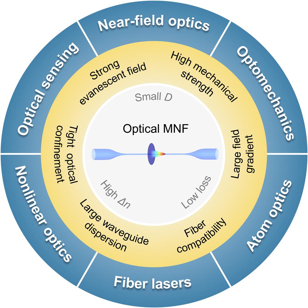
Generally, as the fiber diameter decreases to the subwavelength scale, the MNF exhibits fascinating optical properties that are different from standard optical fibers, including a strong evanescent field, tight optical confinement, surface field enhancement, and diameter/wavelength-dependent large waveguide dispersion[30,58–60]. Also, benefitting from nearly perfect structural and geometric uniformities, glass MNFs possess remarkable mechanical properties, such as high tensile strength (e.g., higher than 10 GPa[61]) and excellent elasticity[61–63], which enable robust and flexible manipulation of freestanding MNFs in various surroundings (e.g., vacuum, gas, or liquid). These favorable optical and mechanical properties, as well as high physical and chemical stabilities of silica glass, make the MNFs a versatile platform for studying light-matter interaction on the micro/nanoscale and developing related photonic technologies [see Fig. 1]. Firstly, the strong evanescent field of the MNF is ideal for studying the near-field interaction between the waveguide mode and matter [e.g., molecules, nanoparticles (NPs), and two-dimensional (2D) materials] located close to the fiber surface, and developing highly efficient near-field coupling techniques (e.g., in/out-coupling of nanowaveguides), as well as functionalization of the MNF itself (e.g., evanescently coupled active or nonlinear materials). Secondly, the tightly confined high-fraction evanescent fields of optical MNFs make the waveguiding field highly sensitive to the refractive-index change of the surrounding environment and/or coupled samples, offering special advantages for high-sensitivity optical sensing on the micro/nanoscale[64–66]. Thirdly, when being squeezed adiabatically from a larger-area mode of a standard optical fiber, the tightly confined field of an MNF mode (i.e., with a very small mode area), is highly favorable for enhancing nonlinear optical effects in the MNF or coupled materials[67–69], as has been widely investigated for harmonic generation[70–72], Brillouin scattering (BS)[73,74], four-wave mixing (FWM)[75], stimulated Raman scattering (SRS)[76,77], and supercontinuum generation[31,78,79]. Fourthly, the waveguide dispersion of optical MNFs is strongly dependent on the diameter or wavelength, offering a compact, flexible, low-loss, and fiber-compatible scheme for dispersion management in nonlinear optics[78,80], pulse compression[81], and fiber lasers[82–84]. Fifthly, by selecting an appropriate diameter-to-wavelength ratio (), a large field gradient in the evanescent field can be generated in the vicinity of the MNF surface, which has been exploited for manipulating micro/nanoparticles[85] and cold atoms[86–88]. Finally, owing to their small mass, optical MNFs can exhibit a sensitive optomechanical response (typically manifested as mechanical vibrations) to the momentum change of the waveguided light fields[89–91], which has been adopted for studying optoacoustic interactions[73,74,92,93] and optomechanical technology[94]. So far, optical MNFs have been attracting broad interest from near-field optics, nonlinear optics, atom optics, and optomechanics to optical nanowaveguides, micro-couplers, resonators, sensors, and lasers.
Sign up for Photonics Insights TOC. Get the latest issue of Photonics Insights delivered right to you!Sign up now
Figure 1.Overall description of optical MNFs in terms of characteristics and applications.
Overall, the past two decades have witnessed an encouraging development of optical MNFs. As a miniaturized fiber-optic platform, optical MNFs not only retain the intrinsically outstanding waveguiding properties of conventional optical fibers, but also offer favorable nanophotonic behaviors. Parallel to the flourishing of fiber-optic technology and nanotechnology in the early 21st century, high-quality glass MNFs have been developed as low-dimensional ultralow-loss optical waveguides on the (sub)wavelength scale, and have been inspiring abundant research interest in multidisciplinary fields from time to time. Previously, MNF optics and applications have been reviewed in many articles[49,50,58–60,65–67,69,84–88,95,96], with most of them focusing on a certain specific research area such as fabrication[49,50], nonlinear optics[67,69], optomechanics[85], atom optics[86–88], passive components[60], optical sensors[64–66], and fiber lasers[84]. There are several comprehensive review articles[58,59] or a monograph[97], but they all have been published for more than 10 years. Now it is the time to give an updated and comprehensive review, to include the latest progress and new insights in this field.
In this regard, we review the development of optical MNFs over the past two decades, with emphases on their fabrication, properties, and applications. The article contains the following six sections: (1) Introduction—a brief introduction to the historical background and a summary of properties and potentials of glass MNFs; (2) Fabrication of Optical MNFs—recent advances in the fabrication of optical MNFs, especially an advanced fabrication technique with real-time high-precision diameter control; (3) Optical Waveguiding Properties of the MNFs—theoretical and experimental waveguiding properties of optical MNFs, including linear and nonlinear optical properties; (4) Mechanical Behavior—elastic and plastic deformation, with emphases on elastic strain and tensile strength of glass MNFs; (5) MNF-Based Applications—from near-field optical coupling, passive optical components, optical sensors, and optomechanics to fiber lasers and atom optics; (6) Conclusion and Outlook—a brief summary of the current status of MNF optics and technology, and an outlook of future challenges and opportunities.
2 Fabrication of Optical MNFs
The materials of optical MNFs are generally divided into glassy or crystal materials. Silica glass, which presents a number of advantages of excellent homogeneity, broadband optical transparency (around 250–2800 nm), high physical and chemical stability, low thermal expansion, temperature-dependent viscosity, and easy remolding, is a typical glassy material for optical MNFs. Historically, since the first glass MNF was drawn from molten quartz by a flying arrow in the late 19th century[1], with the advancement of technology in the first half of the 20th century, silica MNFs were feasible to fabricate from glass in a stable and efficient manner, and their optical properties (e.g., birefringence and bending loss) were investigated[98,99]. After the 1960s, along with the development of standard glass fibers, glass MNFs were routinely taper drawn from glass fibers heated by flame or laser beams[24,100,101], which also facilitated optical launching and handling of the MNFs that were naturally connected to the glass fibers. Meanwhile, mechanized or automated stretching systems were invented to better control the tapering shape and improve the repeatability[18,24]. The emergence of subwavelength-diameter MNFs in the 2000s, especially for waveguide dispersion management and cold atom manipulation, puts forward higher requirements on the diameter accuracy, and mechanized stretching systems with real-time feedback for high-precision diameter control were thus developed.
For glass MNF, high-temperature drawing is the main fabrication technique. When heated, glass becomes viscous[102], making it possible to be drawn into a fiber with a diameter down to nanometer scale. Meanwhile, the high-temperature drawing process bestows the MNF a pristine molten-frozen surface, with an intrinsic surface roughness down to sub-nanometer scale[103–105]. Therefore, compared with other approaches (e.g., chemical etching[106] and excimer laser ablation[107]), the high-temperature drawing technique offers glass MNFs with unparalleled geometric uniformity and surface smoothness (e.g., in surface roughness), which are essential for low-loss optical waveguiding[29,33,34,56]. With the assistance of a scanning heating system (i.e., “flame brush”[18,49,108] and later the “scanning fiber” with a motionless flame[40]), the length of the uniform-diameter MNFs can reach tens of centimeters[40].
Inspired by glass MNFs, other types of optical MNFs have been fabricated from functional materials other than glass. For example, a variety of polymers [e.g., polymethyl methacrylate (PMMA)[109], polystyrene (PS)[110,111], and polyacrylamide (PAM)[112]] or biomaterials (e.g., silkworm silk[113], spider silk[114,115], lotus root silk[116], and Escherichia coli[117]) have been fabricated into MNFs by physical (solution/melt) drawing[109–112], chemical/biological synthesis[113–118], or electrospinning[119], and used to waveguide light for a variety of purposes. In addition, recently, crystal micro/nanoscale wires made of semiconductors[120–123], dielectrics[124,125], or even ice[126] have also been called optical “nanofibers” or “microfibers” when they are used for optical waveguiding, just as we named waveguiding wire-like sapphire single crystals as sapphire optical fibers some 30 years ago[125,127], although they are typically fabricated by bottom-up crystal growth processes[128–132].
This section focuses on high-temperature drawing techniques of glass optical MNFs and the corresponding diameter control and characterization techniques. The fabrication of other types of MNFs can be found in many review articles elsewhere[128–136].
2.1 Taper Drawing of Silica Fibers
The taper-drawing technique is a top-down approach that physically tapers and extends a structure based on its viscosity at a certain temperature or concentration. This technique works for glassy materials (e.g., glass, polymer, or even metals) and can reduce the cross-sectional size of the taper down to nanometer scale, while maintaining an ultra-low surface roughness. Figure 2(a) shows a structural diagram of taper drawing a standard glass fiber by stretching both sides of the heated fiber. When the diameter goes down to the target size, an MNF is obtained with both ends connected to standard fibers through conical transition regions, and this kind of MNF is usually called a “biconical” MNF. The typical taper drawing process and the geometry of the transition region of an MNF can be predicted by a tapering model proposed by Birks and Li[18]. Relying on a flame brush technique, which will be introduced in detail in Section 2.1.1, one can fabricate MNFs with various profiles (e.g., linear, exponential, and sinusoidal) of the transition region for different purposes.
Figure 2.(a) Structural diagram of a biconical optical MNF. SMF, single-mode fiber; , tapering angle of the transition region; , fiber diameter in the transition region. (b) Tapering angle of a typical MNF (black squares) and calculated critical angle (red dots) as functions of local taper diameter at 1550-nm wavelength[40].
The optical loss of the transition region is mostly concerned. As a bridge connecting with a standard fiber pigtail and the MNF, the transition region allows the compression of the propagation light field from 10-μm to sub-1-μm sizes. When the propagation light goes through the transition region, the fundamental mode is progressively waveguided at the silica-air interface as the higher-order modes, leading to continuous weak coupling and interference between the fundamental mode and high-order modes. If the taper angle of the transition region is too steep [ in Fig. 2(a)], a certain fraction of the mode energy will be transferred from the fundamental mode to high-order modes and radiation modes, resulting in a radiation loss and thus reduction of the optical transmittance[137]. To prevent the mode leakage as far as possible, the waveguiding mode should adiabatically couple from the core to the cladding and couple back to the core, suggesting that all the energy remains in the fundamental mode during the mode evolution[16,18,137,138]. The adiabatic criterion for the transition region is[18,138,139]where the left-hand formula represents the characteristic length of the fiber diameter variation with a tapering angle [see Fig. 2(a)], while the right-hand formula represents the beat length between the fundamental mode and one of the high-order modes. is the fiber diameter of the transition region. and are propagation constants of the fundamental mode and the first excited high-order mode (i.e., mode), respectively. Figure 2(b) shows the profile of the transition region of a typical adiabatic MNF. The red dots are the calculated critical angle of the mode, while the black dots, always located below the red dots, represent the actual tapering angles . Under such an adiabatic criterion, the mode-coupling loss can be minimized during the MNF fabrication.
For a standard silica fiber, the softening temperature and annealing temperature are about 1665°C[140] and 1140°C[141], respectively. To draw a silica fiber into an MNF, the heating temperature should be higher than the annealing temperature. Since the viscosity of the fiber is temperature-dependent, the optimal drawing speed for a low-loss MNF varies with the heating temperature. So far, the reported heating temperature for drawing a silica fiber falls between 1160°C and about 1500°C, with a drawing speed ranging from 0.04 mm/s to about 0.5 mm/s, correspondingly[37–46,49,50]. As a reference, for a drawing speed of 0.1 mm/s, the typical heating temperature of the heating source is ranging from 1200°C to 1300°C.
In real fabrication, the precision of mechanical motion components and the stability of the thermal field for fiber heating are crucial to obtain MNFs with excellent diameter uniformities and extraordinary surface smoothness. Also, the choice of heating methods is particularly important for taper drawing different glass materials, as well as for obtaining MNFs with different properties. Currently, there are three heating methods: flame, electric, and laser-heated methods, as introduced below.
2.1.1 Flame-heated taper drawing of glass fibers
The typical fabrication system of the “flame-heated taper drawing” is shown in Fig. 3(a). A fixed gas nozzle, cooperating with a mass flow controller, provides a stable flame (e.g., oxyhydrogen flame[37,142,143] and isobutane-oxygen flame[33]) for heating a standard fiber. Once a bare fiber located at the heating zone reaches a stable temperature, two high-precision translation stages on both sides smoothly draw the fiber into an MNF. Usually, in the case of a fixed hot zone and simply drawing a fiber to both sides, it is challenging to achieve a uniform waist length exceeding 1 cm. As an alternative, the flame brush technique, first used for fabricating fiber couplers[144], has been commonly adopted to fabricate fiber tapers[18] and optical MNFs[58] with larger lengths. Using this fabrication technique and the fabrication system in Fig. 3(a), we can obtain a long-length optical MNF. Figure 3(b) gives the schematic (upper, not to scale) and experimentally measured (bottom) fiber diameter evolution of a typical biconical silica MNF ( in diameter and 9 cm in uniform length), in which the scanning electron microscope (SEM) image [see Fig. 3(b), bottom inset] reveals an extremely smooth surface of the MNF.
Figure 3.Typical flame-heated taper-drawing fabrication system. (a) Photograph of a flame-heated taper-drawing system for fabricating silica MNFs. Inset: close-up image of the flame nozzle. (b) Schematic (upper, not to scale) and experimentally measured (bottom) fiber diameter evolution of a biconical drawn silica MNF along the fiber length[54]. The MNF has a diameter of about 930 nm and a uniform length of 9 cm. The diameter evolution of the tapering region (red circles) was measured by an optical microscope (upper insets), while that of the MNF (blue circles) was measured by a scanning electron microscope (bottom inset).
Typically, the flame brush technique has two configurations. The first is that the flame moves to and fro to heat and scan an optical fiber, while two translation stages move outward to draw the fiber[145,146]. Note that the hydrogen flame may be fluttered by the airflow during the reciprocating motion, resulting in an uneven heating of the fiber. Alternatively, using an electric heater or a laser heater can be much more stable in the scanning process, which is also called as “modified flame brush technique”[58]. In the second type the flame is motionless, while the fiber is scanned and stretched on top of the flame, driven by the translation stages[40]. It is worth mentioning that the excellent stability and smoothness of the moving translation stages are critical to removing uncertainties and obtaining a high-quality MNF in the taper-drawing process. In recent years, with the development and widespread adoption of high-precision, high-stability, and highly controllable translation stages, the uncertainties in the MNF fabrication, especially in the second configuration, have been effectively suppressed.
With these improved fabrication systems, MNFs with low loss, large length, and high diameter uniformity can be routinely obtained. For instance, in 2014 Hoffman et al. achieved an optical transmittance as high as in a single-mode MNF (500 nm in diameter and 5 mm in length) at 780-nm wavelength[37], corresponding to a loss as low as . In 2020, Yao et al. reported a 99.4%-transmittance low-loss MNF with a diameter of 1.2 µm, diameter uniformity of , and a length of 10 cm at 1550-nm wavelength[40].
Typical optical and electron microscope images of as-fabricated MNFs are shown in Fig. 4. Figure 4(a) shows a bright-field optical microscopic image of a 550-nm-diameter silica MNF. Although measuring the accurate diameter of such a thin MNF is beyond the capability of conventional optical microscopy, the diameter uniformity and the defect-free surface of the MNF can be clearly observed. To examine the MNF with a higher resolution, electron microscopes are typically adopted. Figures 4(b)–4(e) present SEM images of as-fabricated silica MNFs, manifesting excellent diameter uniformities with fiber diameter down to 30 nm [see Fig. 4(b), a bundle of MNFs with diameters of 140, 510, and 30 nm, respectively], extraordinary surface smoothness [see Fig. 4(c)], long length [see Fig. 4(d)], and outstanding mechanical strength [see Fig. 4(e)]. To investigate the surface roughness of optical MNFs, a higher-magnification transmission electron microscope (TEM) can be used. Figure 4(f) gives a TEM image of a 330-nm-diameter MNF[29], obtaining a root-mean-square roughness of about 0.2 nm, which is much better than all other types of subwavelength-diameter/width optical waveguides. The electron diffraction pattern [see the inset of Fig. 4(f)] manifests that the silica MNF is amorphous.
Figure 4.Structural characterization of silica MNFs. (a) Optical microscope image of a 550-nm-diameter silica MNF. SEM images of (b) self-supporting bundle of MNFs assembled with silica MNFs with diameters of 140, 510, and 30 nm[97], (c) 790-nm-diameter silica MNF with a smooth surface, (d) coiled 260-nm-diameter silica MNF with a total length of about 4 mm[29], and (e) 360-nm-diameter silica MNF with a bending radius of 3 µm[95]. (f) TEM image of the surface of a 330-nm-diameter silica MNF[29]. Inset: electron diffraction pattern of the MNF.
However, the flame-heated configuration has some limitations: (1) the flame will cause airflow disturbance to the MNF, especially to the MNF with a diameter of a few hundred nanometers or less; (2) the combustion byproducts may adhere to the surface of MNFs, resulting in the surface contamination. To address these issues, one may use other types of heating sources.
2.1.2 Electrically heated taper drawing of glass fibers
Compared with the flame, the electric heater not only provides a more stable temperature environment with minimal airflow disturbance and contamination, but also offers an opportunity to draw fiber in the atmosphere other than air (e.g., argon and nitrogen), and can thus effectively isolate the glass from oxygen or when needed. Also, by controlling the supply current, the heating temperature can be controlled much more precisely and conveniently than the flame. Figure 5 shows photographs of typical electric heaters used for drawing glass MNFs. For high-temperature operation (e.g., ), the optional materials for heating elements are silicon nitride, silicon carbide, platinum, and metal alloy wires (e.g., FeCrAl). Besides silica fibers, the electric heating method is also suitable for taper drawing MNFs from other types of glass fibers, especially soft glass with relatively low softening temperatures [see Fig. 5(b)][55,147,148]. More recently, using a wide-zone electric heater, a parallel fabrication technique of silica MNFs has been reported[149], which enables simultaneous drawing of multiple MNFs with almost identical geometries. However, it should be mentioned that compared to the flame, the electric heating element will inevitably suffer from aging when operating at high temperatures (e.g., ) in the long term, and thus usually has a limited lifespan (e.g., hundreds of hours).
Figure 5.Typical electric heaters in fiber-drawing systems. Photographs of (a) a ceramic heater for drawing silica MNFs (NTT-AT, CMH-7022) and (b) a self-designed U-type copper heater for drawing soft-glass MNFs.
In the far-infrared spectrum, silica glass exhibits significant optical absorption. Therefore, a 10.6-μm-wavelength laser can be used for pollution-free heating and drawing fibers[150,151]. Previously, a direct laser-heating approach was adopted for fabricating silica MNFs with relatively large diameters (e.g., several micrometers). For example, in 1999 Dimmick et al. used a laser beam [13 W in power and 820 µm at half-maximum (FWHM) in a focused spot size] to fabricate MNFs with diameters down to 4.6 µm[24]. However, due to the Mie scattering, the effective absorption decreases with a reduced fiber diameter. Consequently, when the fiber diameter goes down to a certain value at which the effective heating temperature of the MNF drops below the allowable drawing temperature, the drawing process is forced to stop[24,150]. Typically, with a reasonable laser power (e.g., less than 1 kW), the minimum diameter of the MNF obtained by this direct laser-heating approach can hardly go below 1 µm. To draw thinner MNFs with a laser-heating system, an indirect laser-heating approach can be used. In 2004, using a sapphire tube to absorb the laser beam and create a stable high-temperature zone for heating a fiber, Sumetsky et al. successfully fabricated MNFs with diameters less than 100 nm[152]. Such an indirect laser-heating configuration offers the flexibility to adjust the heating temperature by the laser power and temperature distribution by the tube geometry. More recently, using micro-sized plasmonic heaters (i.e., pieces of metal plates), Jia et al. obtained nonadiabatic optical MNFs with steep tapering angles and ultra-short transition regions (e.g., a few tens of micrometers)[153]. Owing to the compactness of the fabrication system, the taper-drawing process can be carried out inside an SEM chamber and in-situ monitored with a high resolution.
2.1.4 High-precision diameter control and measurement
High-precision diameter control is essential to avoid radiation loss in the tapering transition region, as well as to field distribution and waveguide dispersion management in the uniform MNF for applications ranging from near-field optical coupling[154], optical sensing[65,66], and harmonic generation[71] to pulse compression[81,84] and atom trapping[86–88]. To date, the most frequently adopted method is real-time feedback control by monitoring the intermodal interference and high-order-mode cutoff during the fabrication process[38,39,45]. In 2014, Yu et al. first reported a diameter-control method with feedback by monitoring the cutoff of the mode in the intermodal interference[45], showing a diameter error of less than 2%. Later in 2017, Xu et al. demonstrated a feedback control of the MNF diameter by monitoring the drops of high-order modes at 785-nm wavelength, stopping the drawing process after a certain time according to the constant hot-zone model, and obtaining a precision better than 5 nm for fiber diameters in the range of 800–1300 nm[38]. More recently, Kang et al. improved the diameter-control technique by employing a white-light source as the probing light, real-time monitoring, and immediately stopping the drawing process at the cutoff of the mode[39], and realized a precision of about with fiber diameters from 360 to 680 nm. Figure 6 shows the real-time diameter control of the taper drawing a 360-nm-diameter MNF by monitoring the -mode cutoff at 532-nm wavelength. Once the abrupt intensity drop for the mode is observed, the MNF pulling process is terminated instantly.
Figure 6.Schematic diagram of the diameter-control technique in the fabrication of a silica MNF based on the mode-cutoff feedback[39].
With the above-mentioned high-precision diameter control technique, MNFs with accurate diameters and excellent diameter uniformity can be fabricated with good reproducibility, which have found applications in MNF Fabry-Pérot (FP) cavities[53] and high-efficiency harmonic generation[54]. Besides the high-order-mode cutoff, the scattering intensity of waveguiding evanescent fields has also been used for real-time diameter control[52]. Also, the diameter uniformity and control accuracy can be further improved by optimizing the heating condition, feedback system, and mechanical performance of the fabrication system.
In addition, it is worth mentioning that, driven by the demand for in-situ diameter measurement of the MNF, a number of non-destructive optical methods have been reported over the last 20 years. For example, in 2004 Warken and Giessen demonstrated that the profile of subwavelength-diameter MNFs could be measured by the diffraction pattern, with a resolution of over a length of 5 cm[155]. Similarly, a series of optical microscopy techniques have also been reported for measuring the MNF diameter with a resolution of below 50 nm[156–159]. In 2006, Sumetsky et al. proposed a fiber-assisted scanning detection technique for probing the surface and bulk distortions of optical MNFs[160]. By scanning a partly stripped 125-μm-diameter fiber along an MNF and detecting the optical transmission of the MNF, sub-nanometer measurement accuracy of the MNF diameter was realized. Besides, many other techniques based on external gratings[161,162], near-field probing[52,163–165], stress-strain analysis[62], Rayleigh scattered light imaging[166,167], optical backscattering reflectometry technique[168], short-time Fourier transform analysis on the modal evolution[169], second- and third-harmonic generation[170], and forward BS[171], with a resolution from 15 nm to 40 pm, have been reported in recent years.
2.2 More Fabrication Techniques
The aforementioned technologies primarily use standard fibers as preforms for fabricating MNFs with mechanized systems. However, not all materials can be obtained in fiber forms, especially those actively functionalized glass or polymer materials. Therefore, several other fabrication techniques, including drawing MNFs directly from bulk pieces of glass[56], polymer solution[112,172–174], or melt[175–177], have been reported in recent years. Meanwhile, the fabrication of glass MNFs using chemical etching[106] and electric arc[178–180], and polymer MNFs using chemical synthesis[118], electrospinning[119], and nanolithography[181], has also been demonstrated. In addition, bottom-up synthesized techniques, originally for growing crystalline whiskers[182], have also been improved for growing highly uniform single-crystal photonic semiconductor micro/nanowires (also called MNFs recently)[136,183,184], oxide nanowires[185–187], or even ice microfibers[126], for low-loss optical waveguiding. As most of these techniques have been reviewed elsewhere[128–136], limited by the space of this article, we will not go into detail.
3 Optical Waveguiding Properties of the MNFs
For guiding light on the micro/nanoscale, optical waveguiding behaviors are the most concerned properties of the MNFs. Since the first waveguiding model of the dielectric cylinders[4], so far, comprehensive theoretical models have been established for both linear and nonlinear optical waveguiding in MNFs. Incorporated with versatile numerical calculation software products (e.g., MATLAB, Mathematica, COMSOL, and Ansys Lumerical FDTD), waveguiding behaviors of complicated MNF-based structures (e.g., bending loss in bent MNFs[188,189], near-field coupling between multiple MNFs[190–194], output endface patterns[195], and strong mode-coupling-induced ultra-confined optical fields[196–198]) can now be obtained with a high precision. Meanwhile, along with the fast-developed experimental techniques for the manipulation and characterization of individual MNFs, the optical properties of MNFs have been measured and engineered experimentally. The first half of this section aims to provide a comprehensive understanding of the waveguiding behaviors in subwavelength-diameter MNFs based on analytical and numerical approaches. In the latter half of the section, we mainly discuss and summarize recent advances in optical waveguiding properties.
3.1 Fundamental Waveguide Theory of Optical MNFs
Due to the large index contrast between the core of subwavelength-diameter MNFs (e.g., for silica) and surrounding (e.g., for air), it is difficult to calculate the propagation light field using weakly guiding approximation. The most frequently used method is solving for the propagation constants based on exact solutions of Maxwell’s equations and numerical calculations[30]. Generally, an as-fabricated optical MNF possesses an extremely uniform diameter, smooth surface [see Figs. 4(a), 4(c), and 4(f)], and perfect circular cross section [see Fig. 7(a)], which are also well-defined in the theoretical model. The length of the MNFs (typically ) is large enough to establish the spatial steady state, and the MNF diameter (, typically ) is not very thin so that the macroscale parameters of permittivity () and permeability () can be used to describe the responses of a dielectric medium to an incident electromagnetic field. The MNF is assumed to have an infinite air-clad with a step-index profile (i.e., two-layer structure), which is expressed as where and are the refractive indices of the MNF core and the surrounding, respectively. It is worth noting that for MNFs with more layers of index profiles, a multiple-layer-structured cylindrical waveguide model should be employed[199–201]. For non-dissipative and source-free MNF materials, Maxwell’s equations can be reduced to the following Helmholtz equations[30,202]: where , is the vacuum wavelength of the transmitted light and is the propagation constant. Given the perfect circular cross section of a subwavelength-diameter MNF, Eq. (3) can be analytically solved in the cylindrical coordinate and the eigenvalue equations for the and modes are obtained as[30,203]for the modes: and for the modes: with the normalized transverse wave numbers and given by with the -number given by where is the Bessel function of the first kind and is the modified Bessel function of the second kind.
Figure 7.Calculation of waveguiding modes in optical MNFs. (a) SEM image of a 400-nm-diameter tellurite glass MNF with a circular cross section[56]. (b) Calculated propagation constant () of waveguiding modes in an air-clad silica MNF at a wavelength of 633 nm[30]. Solid line: fundamental mode. Dotted lines: high-order modes. Dashed line: critical diameter for single-mode operation. (c) Electric fields of several waveguiding modes in a 600-nm-diameter silica MNF at 633-nm wavelength. (d) SEM image of a 900-nm-diameter CdS nanowire with a hexagonal cross section[208]. and are the diagonal-circle approximation diameter and circular-area-equivalence diameter for nanowires with different cross sections, respectively.
By numerically solving the eigenvalues of Eqs. (4)–(6), the propagation constants of waveguiding modes supported by a circular-cross-section MNF can be obtained [see Fig. 7(b)]. The diameter-dependent waveguiding properties of air-clad silica MNFs at 633-nm wavelength are presented. One can clearly see that when the MNF diameter reduces to a certain value [denoted as a dashed vertical line in Fig. 7(b), corresponding to the -number to be 2.405], only the fundamental mode (i.e., mode) exists and higher-order modes are effectively suppressed. In other words, the -number can be used to evaluate whether an MNF is operated at a single mode for a given wavelength. In principle, for the case of single-mode operation in a subwavelength-diameter MNF, the electric field of the mode is quasi-linearly polarized. Specifically, the transverse component of the field is linearly polarized in time at each fixed local point, while the total electric field vector rotates elliptically with time, in a plane parallel to the MNF axis[88,204]. The transverse component inside the MNF is not only linearly polarized in time but also almost linearly polarized in space, while the orientation angle of the transverse component outside the MNF varies in space. To maintain the polarization state in the waveguiding mode field of a subwavelength-diameter MNF, several methods have been developed including using scattering imaging[205,206] and directional coupling[207]. Additionally, it is widely known that standard fiber falls in the regime of paraxial or weakly guiding, and thus the description of waveguiding modes can be greatly simplified using degenerated linearly polarized (LP) modes. However, due to the large index contrast, the waveguiding modes in an optical MNF are non-degenerate with complex polarization properties. To observe the light field distribution intuitively, Fig. 7(c) shows electric fields of several waveguiding modes in a 600-nm-diameter silica MNF including , , , and modes at 633-nm wavelength. It is worth mentioning that 1D crystalline nanowires, usually polygonal in cross section [see Fig. 7(d)], are also widely used as nano-waveguides. To quickly and accurately estimate their waveguiding properties (e.g., propagation constants), Bao et al. proposed a circular-area-equivalence scheme to treat a polygonal-cross-section nanowire as a circular MNF with an equivalent cross-section area[208], and showed its advantages of simplicity, intuition, high accuracy, and versatility in numerical calculation, even for cross sections with fewer sides. Following the fundamental waveguide theory above, we can judiciously investigate and design the optical waveguiding properties of optical MNFs.
3.2 Basic Optical Waveguiding Properties
3.2.1 Evanescent field and optical confinement of waveguiding modes
When the fiber diameter goes down to the subwavelength scale, the light waveguided in an MNF contains an evanescent wave carrying a significant fraction of the power, which penetrates a certain distance outside the core. The power distribution in an optical MNF can be written by the time-averaged Poynting-vector component along the -axis[30,69,202]: where and represent spatial distributions of electric and magnetic fields, respectively, and denotes a unit vector in the -direction.
For the fundamental mode, the -component of the Poynting vector is obtained as inside the core (): and outside the core (): with
The fractional power inside the core (i.e., the percentage of the confined light power inside the core) is defined as with .
For reference, Fig. 8(a) presents the power distribution of the mode at 633-nm wavelength in silica MNFs with diameters of 800, 400, and 200 nm[32,59], clearly showing the increasing fractional power outside the fiber core with decreasing fiber diameter. While an 800-nm-diameter MNF exhibits good optical confinement at 633-nm wavelength with major energy inside the core, a 200-nm-diameter MNF leaves a large amount of light ( in power) outside the core as evanescent waves. For optical and photonic applications, a tight optical confinement is beneficial for reducing the modal diameter and increasing the integrated density of optical circuits with less crosstalk, while a large evanescent field is helpful for near-field energy exchange between the MNFs and other 1D optical waveguides within a short interaction length, as well as for improving the sensitivity of the MNF-based sensors and optomechanical devices.
Figure 8.Optical waveguiding properties of silica MNFs. (a) -direction Poynting vectors of the fundamental mode in silica MNFs with different diameters at 633-nm wavelength in 3D view (upper row) and 2D view (lower row)[30,32]. (b) Diameter dependence of the waveguide dispersion of fundamental modes in silica MNFs at the wavelengths of 633 nm and 1.5 µm, respectively[30]. (c) Calculated longitudinal electric-field intensity distribution of two evanescently coupled parallel 350-nm-diameter silica MNFs at 633-nm wavelength[154]. The overlapping length between two MNFs is 4.8 µm. (d) Schematic diagram of two evanescently coupled identical parallel MNFs (upper row)[190]. The lower row shows calculated cross-sectional electric-field intensity in the - and -polarizations of fundamental modes in the MNF ( or 2). The radius of two identical MNFs is 200 nm, and the input light wavelength is 800 nm. (e) Schematic illustration of the crosstalk in two intersecting silica MNFs[213]. (f) Calculated output patterns of 400-nm-diameter silica MNFs with flat, 30°-tapering-angled, and 60°-tapering-angled endfaces in air[195]. The input light wavelength is set to be 633 nm. The white-line rectangles in (c) and (f) map the topography profile of the MNFs.
As the subwavelength-diameter MNF enables a considerably high fraction of the mode power outside the core, a strongly diameter-dependent waveguide dispersion can be achieved with a magnitude much larger than that in a standard fiber. The group velocity dispersion (GVD, ) of an optical MNF is defined as with group velocity given by
Based on Eqs. (14) and (15), Fig. 8(b) gives the dispersion of the fundamental mode in air-clad MNFs as a function of the MNF diameter at the wavelengths of 633 nm and 1.5 µm[30]. One can clearly see that the GVD in the normal dispersion regime can go up to ns/(nm·km) level, while that of the weakly guided glass fibers is on the order of tens of ps/(nm·km). Moreover, the large waveguide dispersion in an MNF can also dominate over the material dispersion. To be specific, of an 800-nm diameter MNF is about at 1.5-μm wavelength, which is times larger than that of the material dispersion. Therefore, we can finely tailor the total dispersion (combined material and waveguide dispersions) to be zero, positive, or considerably negative by controlling the MNF diameter and length. In practice, effective dispersion management using subwavelength-diameter MNFs has been widely applied for supercontinuum generation[78,80], FWM[75], ultrafast fiber lasers[82,83,209,210], and quantum optics[211,212].
3.2.3 Near-field coupling and crosstalk between two MNFs
The aforementioned waveguiding properties are basically appropriate for single optical MNFs. The investigation of the mutual interaction of waveguiding modes between two optical MNFs is also important for photonic applications. When two parallel MNFs are in close contact, the evanescently coupled MNFs with high index contrast cannot be treated as weakly coupled systems. In this case, it is difficult to perform the calculation analytically and thus numerical methods are more appropriate. In 2007, Huang et al. investigated evanescent coupling between two air-clad parallel MNFs by means of the finite-difference time-domain (FDTD) simulation[154]. Figure 8(c) presents the longitudinal electric-field intensity distribution of two parallel evanescently coupled silica MNFs (350 nm in diameter) at 633-nm wavelength. For the case of two parallel MNFs with a certain distance [see Fig. 8(d), upper row], Le Kien et al. investigated the coupling of fundamental waveguiding modes in two identical parallel MNFs based on the coupled mode theory[190]. The lower row of Fig. 8(d) shows the cross-sectional profiles of the electric-field intensity distributions at 800-nm wavelength in the - and -polarized fundamental modes of a single MNF (400 nm in diameter), which are symmetric with respect to the principal axes and . On this basis, Le Kien et al. studied the optical force and optical trap of an atom around the middle between two coupled identical parallel MNFs over the next few years[191–193]. The optical forces between the MNFs were attractive for the fields of symmetric modes (i.e., even modes) and repulsive for the fields of antisymmetric modes (i.e., odd modes). For a ground-state cesium atom around the middle of two coupled identical parallel optical MNFs, a net trapping potential with a significant depth of about 1 mK, a large scattering-limited coherence time of several seconds, and a large recoil-heating-limited trap lifetime of several hours can be obtained by properly choosing realistic parameters. Such a twin-MNF structure can also be used for highly efficient single-photon collection, with optimal coupling efficiency [194]. When the mode overlapping and coupling between two nanowaveguides exceed a certain degree, strong mode coupling occurs. In 2022, in a coupled nanowire pair (CNP), Wu et al.[196] reported strong mode coupling induced slit waveguiding mode, in which an ultra-confined optical field was generated with an optical confinement down to sub-1-nm level () and a peak-to-background ratio of . Shortly after, Yang et al. proposed a waveguiding scheme to generate such a sub-nanometer-confined optical field using a tapered optical fiber[197], showing great flexibilities for narrow linewidth, broadband tunability, and ultrafast pulsed operation. More recently, Yang et al. reported a similar mode-coupling-induced nano-slit mode in a coupled glass MNF system, showing the possibility of generating a sub-nm-thick blade-like optical field[198]. With the same scale as a small molecule, this kind of confined optical field is promising for super-resolution nanoscopy, atom/molecule manipulation, and ultra-sensitive detection.
Besides parallel MNFs, coupling between two intersecting MNFs has been investigated. In 2019, Li et al. investigated the crosstalk between two intersecting optical MNFs[213], as schematically shown in Fig. 8(e). When the intersection angle is large enough (e.g., ), the crosstalk of two single-mode MNFs can be better than . For a perpendicular intersection (i.e., intersection angle of 90°), the crosstalk is minimized to be better than . Meanwhile, the crosstalk is not only intersection-angle-dependent, but also related to the MNF diameter and separation of two MNFs. Following these results, it is possible to design a close arrangement of the optical MNFs with acceptable crosstalk.
3.2.4 Endface output patterns
As a kind of quasi-1D optical waveguide structure on the micro/nanoscale, glass MNFs with diameters smaller than the light wavelength are promising for tailoring endface output patterns, which is highly desirable in many photonic applications like subwavelength-dimension light beams[214], optical probes[215], and point sources[216,217]. In 2007, Ma et al. exploited a near-field scanning optical microscope (NSOM) to scan the endfaces of glass MNFs (including silica and tellurite MNFs) and obtained the endface output patterns of the MNFs on a substrate[218]. To further investigate the longitudinal-field-intensity distribution of the MNFs, Wang et al. numerically calculated the output patterns of the MNFs at 633-nm wavelength by means of a three-dimensional finite-difference time-domain (3D-FDTD) approach[195]. For reference, Fig. 8(f) shows the calculated longitudinal field-intensity distribution of 400-nm-diameter MNFs with flat and tapered endfaces. Compared with standard optical fibers, glass MNFs possess much lower reflectance (e.g., with a flat endface, the reflectance is about 2% in glass MNFs and 4% in standard optical fibers). For the MNFs with tapered endfaces, the light output from the tapered tip spreads out symmetrically along the propagation direction. Interestingly, the smaller tapering angle yields a larger divergence of the output from the tapered tip, which is well suitable for the generation of point sources.
3.3 Optical Loss
For standard single-mode fibers, the minimum transmission loss (e.g., 0.14 dB/km at 1550-nm wavelength[219]) is generally determined by the fundamental scattering and intrinsic absorption of silica glass. As the diameter decreases to the subwavelength scale, due to the decreased mode area, a high-fraction evanescent field, and normally open-air clad of the MNFs, the optical transmittance is very sensitive to a number of factors, including surface roughness, diameter fluctuation, surface contamination, and micro-bending, resulting in an overall loss much higher than that of a standard silica fiber. Fortunately, in the past 20 years, benefitting from the great progress in the fiber fabrication and protection techniques, the optical loss of an MNF has been significantly reduced.
3.3.1 Scattering loss
For a subwavelength-diameter optical MNF with a clean surface, the scattering loss mainly arises from the surface roughness. To be specific, the molten-drawn process of the MNFs thermally activates capillary waves that are frozen onto the surface at the glass transition temperature, inevitably leading to quasi-long-range correlations in the surface height (i.e., surface roughness)[103–105,220–222]. By a roughness-induced current model, in 2007 Zhai and Tong numerically calculated the roughness-induced scattering loss of silica, tellurite, phosphate, and silicon MNFs with sinusoidally perturbed surfaces[223]. As shown in Fig. 9(a), with the same roughness amplitude, the loss coefficient exhibits an oscillating dependence on the perturbation period, indicating that the distribution of the perturbation period (i.e., the correlation length) should be determined for accurate estimation. Shortly after, by treating the perturbed surface as a random field and determining the radiated power with averaging over the perturbation ensemble, Kovalenko et al. investigated the radiation losses of optical MNFs with random rough surfaces in the assumption of Gaussian statistics, and estimated the loss value based on an inverse-square perturbation power spectrum[224]. Around the same time, by considering the nonadiabatic intermodal transition, Sumetsky investigated the radiation loss of a subwavelength-diameter MNF introduced by a tiny intrinsic nonuniformity, and showed an exponential dependence of the loss on the MNF diameter[225], with an important conclusion that the allowed minimum diameter of an optical MNF is about 1/10 the vacuum wavelength of the guided light. Subsequently, with an experimental test on a tapered fiber, Sumetsky et al. demonstrated that a subwavelength-diameter MNF can exhibit a low loss only if its diameter is larger than a threshold value, which is primarily determined by the wavelength and the characteristic length of the long-range nonuniformity[226]. Later, Hartung et al. determined that a threshold diameter of a 10-mm-long MNF appears to be [227]. In addition, considering that in some cases the MNFs are supported on a substrate, the radiation loss caused by the substrate has also been investigated[228,229]. Generally, to effectively alleviate or eliminate the optical loss induced by the substrate, the MNF should not be too thin and the refractive index of the substrate should be lower than the effective index of the MNF. It is also important to mention that the surface contamination of the MNF will give rise to a further increase in radiation loss[35]. Typically, the contamination originates from electrostatic and diffusive adhesion of ambient microparticles and molecules. Therefore, an isolation of optical MNFs to atmospherical contamination is necessary for practical use.
Figure 9.Optical losses and absorption of optical MNFs. (a) Roughness-induced radiation losses in air-clad MNFs versus the perturbation period[223]. The amplitude of the surface roughness is assumed to be 0.2 nm and the wavelength of the input light is 1550 nm. (b) Mathematical simulation model of a circular 90° bent MNF[188]. Inset: topography profile of the bent MNF. (c) Electric-field intensity distributions in the plane () of a 450-nm-diameter MNF at a wavelength of 633 nm, with bent radii of (I) 5 µm and (II) 1 µm. The output mode profiles of the 5-μm and 1-μm bent MNFs at the P1 transverse cross planes in (b) are shown in (III) and (IV), respectively. The black solid lines map the topography profiles of the MNFs. (d) Bending losses of a 350-nm-diameter silica MNF (I-line, squares), 350-nm-diameter PS MNF (II-line, circles), and 270-nm-diameter ZnO MNF (III-line, triangles) at 633-nm wavelength (quasi- and quasi- polarizations) as functions of the bending radius. (e) Schematic diagram of combined effects of the fiber heating, mechanically tapering, and pulsed laser guiding processes on the structural changes of siloxane rings[234]. Heating and mechanical stretching processes break the six-membered rings into highly strained three-membered rings. Given the bandgap value of silica (), using a laser with photon energy in the range of can break the highly strained three-membered rings and generate oxygen-dangling bonds. (f) Defect-absorption-induced temperature rise of a 1.2-μm-diameter silica MNF as a function of the waveguiding power around 1550-nm wavelength[54].
As freestanding waveguided structures, optical MNFs are required to be bent in some cases. As a benefit of the high-refractive-index contrast between the MNF and surrounding, waveguiding modes can be tightly confined inside the MNF, enabling a low bending loss through relatively sharp bends (e.g., a few micrometers in bending radius). In 2009, Yu et al. numerically calculated the bending loss of optical MNFs with circular 90° bends by means of 3D-FDTD simulations [see Fig. 9(b)][188]. It can be seen in Figs. 9(c) and 9(d) that when waveguiding a 633-nm-wavelength light, a bent silica MNF with a diameter of 350 nm and bending radius of 5 µm has an acceptable bending loss of 1 dB/90°. However, as the bending radius reduces to 1 µm, a serious energy leakage occurs around the bending region [see Fig. 9(c)]. In such a sharp bend, to reduce the bending loss, one has to replace the silica MNF with higher-refractive-index MNFs such as PS and ZnO MNFs [see Fig. 9(d)]. Another possible approach proposed by Yang et al. recently is to rearrange the mode field by placing Au NPs around the inner side of the bent MNF[189]. Owing to the localized surface plasmon resonance (LSPR), a considerable fraction of energy can be confined to the interface of the Au NPs and the optical MNF, leading to a reduction in the bending loss. In addition, it is found that, compared with suspended MNF, in a substrate-supported MNF, the bending radius should be larger to guarantee a low propagation loss[230].
3.3.3 Optical absorption
As is well known, the intrinsic absorption of silica glass is very low in its optically transparent window. However, in the high-temperature taper-drawing process, the six-membered rings of the amorphous silica are likely to deform to three-membered rings (i.e., strained Si-O-Si bonds), as the precursor sites for Si and O dangling bonds [see Fig. 9(e)][231–234]. It has been demonstrated that the surface dangling bonds of the MNFs will be photoactivated by a pulsed laser/high-power CW laser, and act as point defects[54,233,234]. Such point defects can be identified by photoluminescence (PL) emission spectra. The point defects on the MNF surface will give rise to an increase in surface roughness and optical absorption, resulting in additional optical losses. It is worth mentioning that the photothermal effect induced by optical absorption is prominent when the MNFs are operated under high optical power[54]. As shown in Fig. 9(f), an evident temperature rise in a high-power waveguiding MNF was measured using a knot resonator (e.g., the temperature of the MNF operating at 5 W was 152°C).
3.3.4 Progresses in loss reduction in optical MNFs
With the improvement of the fabrication and characterization techniques, the measured waveguiding losses of as-fabricated MNFs, especially of subwavelength-diameter MNFs, have been effectively reduced over the last 20 years. As summarized in Fig. 10, since the first reported experimental loss of at 1550-nm wavelength in a subwavelength-diameter silica MNF in 2003[29], the loss has been reduced quickly to a level of 0.001 dB/mm[31]. In 2014, Hoffman et al. reported the lowest loss of at 780-nm wavelength in a 500-nm-diameter silica MNF[37], which is orders of magnitude lower than all other available nanowaveguides [see Fig. 11]. For long MNFs, in 2020 Yao et al. demonstrated ultra-long subwavelength-diameter MNFs (e.g., 15 cm in length) with optical transmittance as high as 97.5% at 1550-nm wavelength[40]. In the same year, Ruddell et al. reported silica MNFs with diameters below 400 nm and transmission higher than 99.9% at 852.3-nm wavelength[53], which were used for constructing high-finesse fiber FP cavities. Besides silica, optical MNFs made of other glass materials have also been extensively studied. For example, in 2006, Brambilla et al. reported the fabrication of compound-glass (e.g., lead-silicate and bismuth-silicate) subwavelength-diameter optical MNFs[55], with measured losses of to at 1550-nm wavelength. In 2007, Mägi et al. reported an overall tapering loss of 3 dB for a biconical fiber taper (1.2 µm in diameter, 18 mm in MNF length, and 164 mm in total length) around 1550-nm wavelength[57]. In 2012, Baker and Rochette measured a propagation loss of at 1530-nm wavelength in a PMMA-cladded chalcogenide MNF (450 nm in core diameter, 13.7 µm in PMMA-cladding diameter)[235]. More studies on optical loss in chalcogenide MNFs have been reported[236].
Figure 10.Optical losses of silica and MNFs over the last 20 years[29,31,33,37,41–43,53,143,211,235–237].
Although low-loss optical MNFs have been well-developed since their first experimental demonstration, most of them are operated in low-power regions, for example, in CW or averaged power. To further enhance the interaction between the waveguiding mode and matters within the mode field, the most straightforward method is increasing the waveguiding power in the MNFs. Recently, Zhang et al. reported high-power CW optical waveguiding in high-quality silica MNFs around 1550-nm wavelength[54]. As seen in Fig. 12(a), the measured output power () of a 1.1-μm-diameter changes quite linearly with the input power (), and the MNF maintains a high transmittance () with waveguided power up to 13 W and a fiber diameter down to 410 nm (i.e., of the vacuum wavelength). At such high power, the maximum power density inside the MNF can be higher than [see Fig. 12(b)]. The ultralow absorption of the silica fiber (used as the preform), high precision in the taper-drawing process, and high cleanliness of both taper-drawing and testing environment enable 10-W-level optical waveguiding in silica MNFs. Furthermore, there are no predominant single scattering points on the surface of MNFs when waveguiding a high-power CW light, indicating that the upper limit of the waveguiding power in an MNF will be higher. By measuring the power-dependent temperature rise in the MNF, a damage threshold of 70 W was predicted [see Fig. 9(f)].
Figure 12.High-power CW optical waveguiding in subwavelength-diameter silica MNFs[54]. (a) High-power optical transmittance of a 1.1-μm-diameter MNF around 1550-nm wavelength, with a CW waveguided power from 0 to 13 W. (b) Calculated diameter-dependent maximum power density in the MNFs at a waveguided power of 1 W. Insets: cross-sectional power density distribution of 0.5-μm-diameter and 1.1-μm-diameter silica MNFs.
As we discussed previously, the surface contamination of the MNFs (e.g., dust and particulate) will introduce additional optical propagation loss. Generally, the degradation is more prominent as the MNF becomes thinner. For the purpose of long-term usage and stability of glass MNFs, adequate protection is highly desirable. Typically, the package of glass MNFs can be categorized into three types: polymer embedding, air-tight sealing, and vacuum packaging. Polymer embeddingLow-refraction polymer is widely exploited to embed and protect glass MNFs from optical degradation. In 2007, Vienne et al. proposed to embed MNFs in a low-index fluoropolymer matrix, and experimentally demonstrated polymer-embedded MNF resonators with Q-factors of 12000[241]. In 2008, Xu and Brambilla compared the effectiveness of packaging of the MNFs in a perfluoro polymer (i.e., Teflon)[242]. While a bare MNF decreased with a rate of in optical transmittance, the embedded MNF remained basically unchanged within 6 days. After that, a variety of low-loss, low-refractive-index materials have been employed for MNF packaging, including polydimethylsiloxane (PDMS)[243–247], Teflon[248,249], hydrophobic aerogel[250], ultraviolet (UV) curable polymer[251,252], and high-substitution hydroxypropyl cellulose[253,254]. Figure 13(a) illustrates a silica MNF embedded in a PDMS film[247], showing the advantages of a small footprint, high flexibility, and conformability to non-flat surfaces (e.g., a human hand).Air-tight sealingSealing the MNFs inside an air-tight box has also been commonly adopted. For example, in 2021 Bouhadida et al. carried out long-term and repeatable measurements of optical transmittance of a 1-μm-diameter MNF at 1.5-μm wavelength[255]. They found that when the MNF was put in an airtight box, the degradation rate of the optical transmittance was as low as in several months. According to the degradation rate, they predicted an acceptable decrease of in the optical transmittance after more than 4 years. Recently, Zhang et al. transferred an as-fabricated 1.2-μm-diameter MNF into a 3D-printed acrylic box protected by high-purity nitrogen gas [see Fig. 13(b)][54]. The encapsulated MNF shows an ability to waveguide a high-power CW light around 1550-nm wavelength for long-term operation. Specifically, the MNF was tested at 12-W power continuously for 20 min every day for 2 months. Over the whole test period of 2 months, the optical transmittance of the MNF remained around 95%, as shown in Fig. 13(c). Apart from an airtight box, other sealed chambers have also been applied to satisfy various experimental requirements, for example, capillary[256–258] and stainless steel tube[92,259].Vacuum treatingFor atom optics, silica MNFs are usually installed in a vacuum chamber. During the installation procedure, a flux of argon gas is maintained to protect the MNF surface from pollution[260]. After the introduction of atom vapor, one of the major challenges is that the warm atoms will accumulate on the MNF surface, leading to optical scattering of waveguide modes and consequently, a drastic degradation in optical transmission. For instance, Lai et al. reported that the transmission of a sub-500-nm-diameter silica MNF degraded to 1.5% of its initial value in rubidium vapor in a full 2700-s run[261]. In this scheme, the base pressure and temperature in the vacuum chamber were and , respectively. To alleviate the atom accumulation, they designed a heating unit to raise the surface temperature of the MNF, enabling the stable preservation of the MNF with a relatively high optical transmittance () surrounded by a high-density rubidium vapor. Afterwards, Lamsal et al. employed metastable xenon as a promising alternative to rubidium[262,263], in which a sub-500-nm-diameter silica MNF resided in a vacuum chamber backfilled with xenon gas. Using this low-pressure system (around 30 mTorr), they demonstrated a complete lack of optical transmission degradation in a 350-nm-diameter silica MNF over several hours[263].In addition, safe and convenient handling of the MNFs without breaking is also required in experiments. For this purpose, a U-shaped bracket is typically employed for detaching an as-fabricated MNF from the taper-drawing system [see Fig. 13(d)] and transferring it to other places, such as an air-tight box for surface protection [see Fig. 13(e)].
Figure 13.Encapsulation of optical MNFs. (a) Schematic of an MNF embedded in a PDMS film on a glass substrate[247]. Inset: photograph of an MNF-embedded PDMS patch attached to a human hand. (b) Photograph of an optical MNF sealed in an airtight 3D-printed acrylic box, filled with high-purity nitrogen gas[54]. (c) Long-term optical transmission of the MNF presented in (b) around 1550-nm wavelength. The waveguided power of the MNF is 12 W. (d) Photograph of an as-fabricated MNF mounted on a U-shaped bracket, with two standard fiber pigtails fixed on both sides of the bracket through the glue. (e) Photograph of an MNF sealed in an air-tight box.
The above-mentioned optical properties are in the realm of linear optics, in which the induced polarizability has a linear relationship with the electric-field intensity. This is valid only when the power density of the waveguiding modes is low. For a high-power optical waveguiding MNF (in pulsed or high-power CW), the nonlinear effect should be considered, in which the optical response could be described by the relationship[264]where is the vacuum permittivity, is the linear susceptibility, and and are the second- and third-order nonlinear optical susceptibilities, respectively. In the nonlinear optical processes, is associated with second-order nonlinear effects such as SHG, sum-frequency and difference-frequency generation (SFG and DFG), and optical parametric oscillation. is related to third-order nonlinear effects including supercontinuum generation, THG, BS, SRS, FWM, and optical Kerr effect.
As we reviewed in Section 3.2, the tight optical confinement, long interaction length, and large diameter-dependent dispersion make optical MNFs excellent candidates for nonlinear optical processes. For example, the power density of the evanescent field can be enhanced to in a 340-nm-diameter silica MNF waveguiding a 1-W 780-nm-wavelength light[20]. Figure 14(a) shows the wavelength-dependent GVD in silica MNFs. For a given MNF diameter, there is a maximum value of the GVD (on the order of thousands of ) in the normal dispersion region. Generally, the optical nonlinearity of photonic waveguides is described by the nonlinear parameter as[68]where is a nonlinear-index coefficient (for silica, [71]), is the angular frequency, is the speed of light in vacuum, and is known as the effective mode area of the waveguiding modes, which is expressed as[68]
Figure 14.Nonlinear optical properties of optical MNFs. (a) Wavelength dependence of the GVD with different MNF diameters. (b) Nonlinear coefficient of silica MNFs versus the fiber diameter at 532-nm wavelength. Spectra of the (c) SHG and (d) THG in a silica MNF (779 nm in diameter, 7 cm in length) pumped by a 5-W-power CW light[54]. The optimal phase matching of the SHG and THG is achieved at wavelengths of 1558.2 and 1572.5 nm, respectively. SH, second harmonic; TH, third harmonic. Insets of (c) and (d) show optical microscope images of output spots of the SH and TH signals at the output end of the standard fiber connected with the MNF, respectively. (e) Supercontinuum generation in a silica MNF pumped by 532-nm-wavelength ns pulses[31], with output far-field patterns from the MNF at (I) low and (II) maximum powers. The pattern in (II) was passed through 10-nm bandpass filters at the center wavelengths of (III) 633, (IV) 589, and (V) 450 nm.
Figure 14(b) plots the diameter-dependent nonlinear parameter of silica MNFs at a wavelength of 532 nm. It is observed that the 350-nm-diameter MNF has a maximum nonlinear parameter of , and the dispersion coefficient falls in the vicinity of the zero-dispersion region. For comparison, the zero-dispersion wavelength of the silica MNFs can be much shorter than that of a standard optical fiber (around 1310-nm wavelength). Moreover, the zero-dispersion wavelength is also diameter-dependent, which provides great convenience for dispersion management in nonlinear processes. In this subsection, we will provide an overview of the nonlinear optical properties in optical MNFs.
3.4.1 Pulse propagation
Generally, for nonlinear applications, ultrashort pulses with high peak power are used to achieve a high nonlinear conversion efficiency. To study the femtosecond pulse propagation in a subwavelength-diameter optical MNF, in 2004 Kolesik et al. proposed a theoretical model for simulation according to a corrected nonlinear Schrödinger equation[265]. Based on the theoretical framework, supercontinuum generation in optical MNFs can be accurately modeled[79,266]. In 2005, Foster et al. experimentally demonstrated the soliton-effect self-compression of ultrafast pulses from 70 to 6.8 fs[81], corresponding to a compression factor of 10.29 and a quality factor of 0.73. Using a nonlinear-envelope equation, they predicted that self-compression could be further down to single-cycle duration. In 2012, Lægsgaard developed a full-vectorial nonlinear propagation formalism for studying the spectrum evolution of short broadband pulses in fiber tapers[267]. In this method, they proposed a perturbative scheme for interpolating fiber parameters along the taper, which provides higher accuracy. Benefitting from the large effective nonlinearity and broad region of anomalous GVD of the MNFs, one can utilize optical MNFs with specific diameters to compress the pulse.
3.4.2 SHG and THG
Harmonic generation including SHG and THG is a kind of nonlinear optical process, in which new signal sources with short wavelengths can be generated. With the rapid development of fiber technology, fiber-based harmonic generation has received much attention, showing the advantages of small footprint, long interaction length, good stability, and low cost. Generally, the SHG is very weak in a silica fiber due to the central-symmetry nature of an amorphous silica. However, when the fiber diameter decreases to the subwavelength scale, the surface dipole and bulk multipole nonlinearities will contribute evidently to the second-order nonlinearity. The theoretical framework of the SHG in MNFs has been well-studied since 2010[268–270]. For efficient SHG, intermodal phase matching and high mode overlapping are highly desirable. In the small-signal limit, the SHG process can be modeled by the following equation: where and are the amplitudes of the fundamental and SHG modes, is the propagation constant mismatch between the SHG signal and the pump, and represents the overlap between the fundamental and the second-harmonic modes, which is expressed as where is the angular frequency of the SHG signal, is the second-order nonlinear polarization (including both dipole contributions from the surface and multipole contributions from the bulk), is the vector normal to the surface, and the electric and magnetic fields of the SH modes are expressed as and .
In 2013, Gouveia et al. experimentally exploited a 700-nm-diameter silica MNF to realize the intermodal phase-matching SHG, with conversion efficiency up to when pumped with 1550-nm-wavelength pulses (90 W in peak power)[72]. By assembling an MNF into a loop resonator that incorporated the phase-matched region of the MNF, they further improved the efficiency by 5.7 times. Very recently, Zhang et al. proposed to accomplish perfect intermodal phase matching and maximum mode overlapping between the fundamental and the harmonic modes by precisely controlling the fiber diameter and finely tuning input light wavelength. Using an 11.3-W 1558.2-nm-wavelength CW light [see Fig. 14(c)], they demonstrated CW-pumped SHG, with conversion efficiency up to , which is higher than those pumped by short pulses[54]. Besides a single MNF structure, other MNF-based structures have been reported for the enhancement of the SHG effect. For example, in 2013 Luo et al. proposed a slot MNF configuration to enhance surface power density and nonlinearity, showing a 25-fold increase in the SHG conversion efficiency as compared to a circular-cross-section MNF[271]. In 2018, Wu et al. employed an optical MNF coupler to achieve quasi-phase matching by coupling compensation. High-efficiency SHG was experimentally demonstrated, with conversion efficiency four orders of magnitude higher than that of each individual MNF[272].
Compared with the SHG, THG is more widely studied in optical MNFs. In 2003, Akimov et al. demonstrated the THG in a 2.6-μm-diameter silica MNF using 30-fs 1250-nm-wavelength pulses[70]. In the following 20 years, a series of theoretical and experimental studies have been carried out to optimize the conversion efficiency in nonlinear optical processes[71,273–280].
For an air-clad optical MNF with a step-index profile, the third-order nonlinear susceptibility is assumed to be -independent, whose value is constant within the cross section of the MNF while zero outside of the MNF. Then the THG process can be modeled by the following coupled-mode equations[71]: where and are the amplitudes of the fundamental and THG modes, is the mismatch of the propagation constant between the third-order harmonic signal and the pump, and is nonlinear overlap integrals (as defined in Ref. [71]). Among them, and govern the self-phase modulation of the pump and the harmonic signal, is related to the cross-phase modulation, and represents the overlap between the pump and the third-harmonic modes.
To achieve efficient THG in an optical MNF, the intermodal phase mismatch (i.e., the propagation-constant mismatch between the high-order modes of the third-order harmonic signal and the fundamental mode of the pump) should be as small as possible, and the overlap integral should be sufficiently large. In 2005, Grubsky and Savchenko theoretically predicted that with an appropriate MNF diameter, an ideal conversion efficiency could be achieved as high as 50% in a 1-cm-long silica MNF[71]. However, it is difficult to obtain such high efficiency because the inherent nonuniformity of optical MNFs may adversely affect the perfect phase matching. In recent years, several effective approaches to realizing quasi-phase matching between the fundamental pump mode and the third-harmonic modes have been reported by Jiang et al. and Hao et al., such as the employment of a counter-propagating pulse train[277], nonlinear phase modulation[278,279], and mechanical strain[280]. Indeed, the THG conversion efficiency excited by short laser pulses reported so far is basically on the order ranging from to . Additionally, pumped with a high-power CW light, high-efficiency THG could also be observed in a 779-nm-diameter MNF (1572.5 nm in fundamental light wavelength), as presented in Fig. 14(d). When the waveguided power of the MNF was increased to 11.3 W, the conversion efficiency was measured as , falling within the range of typical results obtained with short pulses. Since silica MNFs have the potential to waveguide a higher-power light (both in CW and pulsed), the higher conversion efficiency of the harmonic generation is foreseeable in the future.
3.4.3 Four-wave mixing
The FWM process is a third-order optical nonlinear process containing the creation of signal and idler photons ( and ) and the annihilation of two pump photons ( and ) simultaneously. This process is governed by the conservation of the energy and momentum: , and . The tailorable dispersion characteristics of optical MNFs are beneficial for efficient FWM. In 2012, Li et al. reported for the first time the cascaded FWM in optical MNFs pumped by two synchronized picosecond lasers (around 850-nm wavelength)[75]. They showed that the spectrum range could span from several hundreds of nanometers to almost one octave, depending on the MNF diameter, pump power, and wavelength detuning of the two pumps. In practice, the FWM in an optical MNF has been widely applied in quantum optics and nonlinear optics. For example, in 2013 Cui et al. utilized spontaneous FWM in a 15-cm-long MNF to generate correlated photon pairs[211]. Likewise, in 2019 Kim et al. realized the generation of photon pairs via a spontaneous FWM process using a 12-cm-long 615-nm-diameter MNF[281]. In 2021, Delaye et al. reported the emission of photon pairs by the FWM in a silica MNF, with a high coincidence to accidental ratio and high pair emission rate[212]. On the other hand, Abdul Khudus et al. demonstrated parametric amplification through the FWM in silica MNFs with a wavelength band over 1000 nm in 2016[282].
3.4.4 Brillouin scattering
BS is known as a third-order nonlinear process that involves the interaction between an electromagnetic wave and an acoustic wave. An incident photon at frequency is scattered into an up- or downshifted photon with frequencies depending on the phase-matching condition, where frequency is the frequency of the acoustic field. Since its discovery in optical fibers in 1972[283], the BS has been extensively studied in both fundamental and applied sciences[284]. Over the past decade, the advent of optical MNFs has driven immense scientific interest in studying the photon-phonon interaction in subwavelength-dimension structures. Compared with standard optical fibers, optical MNFs with low dimension and hard mechanical boundary conditions enable the enhancement of optical nonlinearity and tightly confined modes of both photons and phonons. It has been reported by Beugnot et al. in 2014 that in a subwavelength-diameter MNF, two kinds of acoustic modes will be excited during the backward BS process: hybrid acoustic wave (HAW) and surface acoustic wave (SAW) modes[73]. The SAWs propagate at a velocity between 0.87 and 0.95 of a shear wave velocity (for fused silica, ), leading to new optical sidebands down-shifted from 6 GHz in the spectrum. The HAWs propagate at an intermediate speed between shear and longitudinal waves with acoustic frequencies of . Interestingly, the SAWs in the MNFs are inherently sensitive to surface features and defects, which offers attractive potential for optical sensing, detection, strain measurement, and optomechanics[63,74,92,285]. Another novel effect, the so-called BS self-cancellation, was demonstrated experimentally by Florez et al. in 2016[286]. Specifically, they scanned the MNF diameter to precisely control the acoustic and optical mode profiles, where the photo-elastic and moving-boundary effects canceled out exactly. In 2018, Chow et al. utilized a phase correlation distributed Brillouin approach to experimentally demonstrate the presence of surface and hybrid acoustic waves at distinct fiber locations[287]. Apart from the backward BS, the forward BS in silica MNFs has been investigated over the last few years[171,288,289]. In 2018, Jarschel et al. constructed a pump and probe forward BS setup to excite the fundamental torsional-radial acoustic mode in a silica MNF[171]. The frequency shift of the torsional-radial acoustic mode can be used to characterize the MNF diameter, as has been mentioned in Section 2.1.4. After that, two theoretical frameworks were reported by Cao et al. on the inter-mode forward BS[288] and Brillouin gain characteristics[289] in silica MNFs. Very recently, Xu et al. realized strong forward intermodal optomechanical interactions in a few-mode optical MNF, with long phonon lifetimes () and strong coupling ()[93].
3.4.5 Stimulated Raman scattering
The SRS is an inelastic third-order nonlinear process in which energy is transferred from input photons to molecular vibrations. Unlike the stimulated BS with a photon-to-acoustic phonon process, the SRS involves a photon-to-optical phonon interaction. In the SRS process, a Stokes (anti-Stokes) photon at a longer (shorter) wavelength with respect to the pump wavelength will be generated. As discussed in Section 3.2, subwavelength-diameter optical MNFs possess a high-fraction evanescent field with high optical intensity. Such a unique evanescent field can create a strong interaction with external materials (with high Raman gain). By this way, in 2013 Shan et al. theoretically investigated[76] and experimentally achieved[77] the SRS in a liquid (e.g., ethanol and mixture of toluene and ethanol) pumped by the evanescent fields of silica MNFs. In 2019, Bouhadida et al. developed the external Raman conversion efficiency to 60% with high reproducibility by optimizing the MNF diameter[290]. Besides the liquid surroundings, the evanescent-wave SRS can also be achieved with a silica MNF immersed in the gas. It has been reported by Qi et al. in 2019 that the SRS efficiency of an MNF surrounded by hydrogen gas is orders of magnitude higher than that in a hollow-core photonic crystal fiber[291]. Relying on the SRS spectroscopy, a novel optical sensing and detection technique with fast response, high sensitivity, and wide dynamic range is on the rise.
3.4.6 Supercontinuum generation
Supercontinuum generation is a kind of complex optical nonlinear process that involves self-phase modulation, Raman scattering, and FWM. Since its first experimental observation in borosilicate glass in 1970[292], the supercontinuum generation has received extensive attention. In 1976, Lin and Stolen demonstrated supercontinuum generation in a 19.5-m silica fiber using a 20-kW 10-ns dye-laser pulse[293]. In principle, to generate a supercontinuum source with a wide spectral range in an optical waveguide, the high optical power density of waveguiding modes, high optical nonlinearity of the waveguide, long nonlinear interaction length, and flat zero-dispersion region are required. The flexibly controllable dispersion and high nonlinear parameter of subwavelength optical MNFs just satisfy these demands[265,294] [see Figs. 14(a) and 14(b)]. In 2004, Leon-Saval et al. reported that supercontinuum spectra with a 400-nm broadening could be observed from 20-mm-long sub-micrometer optical MNFs pumped by 532-nm-wavelength ns pulses[31]. When the peak power is sufficiently high, a significant broadening of the supercontinuum spectrum occurs and the supercontinuum white-light source can be extracted from the output endface of a standard fiber connected with a silica MNF [see Fig. 14(e)]. Afterwards, supercontinuum generation in silica MNFs has been studied at the central wavelengths of 800[79,295] and 1064 nm[78]. From the numerical simulation, Hartung et al. also reported the possibility of using optical MNFs with normal dispersion behavior for coherent supercontinuum generation at deep-UV wavelengths[80]. The short length of the employed silica MNFs allows a low loss in the UV-wavelength edge, making them ideal candidates for deep-UV supercontinuum generation. Meanwhile, chalcogenide glasses have broadband intrinsic transparency (0.5 to 25 µm) and high optical nonlinearity (for the , [296]) for supercontinuum generation from visible to infrared ranges.
Compared with silica MNFs, the chalcogenide MNFs taper drawn from standard chalcogenide fibers show greater potential in nonlinear optics. Besides the UV and visible spectrum regions, NIR and mid-infrared (MIR) supercontinuum sources generated from highly nonlinear chalcogenide-glass MNFs have received a lot of attention in the past 20 years. In 2008, Yeom et al. first demonstrated low-threshold supercontinuum generation around 1550-nm wavelength using an MNF. In the following years, several interesting investigations on the NIR supercontinuum generation in chalcogenide-glass MNFs have been reported[297–299]. For the MIR supercontinuum generation, Marandi et al. achieved a spectrum broadening from 2.2 to 5 µm at 40 dB below the peak in 2012[300]. In 2014, Al-kadry et al. demonstrated two-octave MIR supercontinuum generation from 1.1 to 4.4 µm at [301]. In 2015, using a 15-cm-length chalcogenide MNF (1.9 µm in core diameter), Sun et al. realized the supercontinuum generation spanning from 1.5 µm to beyond 4.8 µm at [302]. In 2017, Hudson et al. coupled 4.2-kW-power pulses into a polymer-protected MNF and successfully demonstrated a spectrum spanning from 1.8 to 9.5 µm at points (2.4 octaves)[303]. In the same year, Wang et al. reported a broadband spectrum spanning from 1.4 to 7.2 µm in chalcogenide tapered fibers pumped in the normal dispersion regime[304]. The generated MIR supercontinuum sources have found important implications in the applications of molecular spectroscopy, MIR frequency comb, early cancer diagnosis, and remote sensing[147,305,306].
4 Mechanical Behavior
As an important property of an optical MNF, the mechanical behavior, basically depending on the material used, is different from that of standard optical fibers with typical diameters around 125 µm. Generally, similar to mechanical behaviors of many other 1D nanostructures that have been extensively investigated[307–310], owing to the decreased defect size and density with decreasing fiber diameter, the silica MNF demonstrates enhanced mechanical properties regarding tensile strength and allowed strain, which is beneficial for flexible manipulation, characterization, and functionalization of the MNF. Meanwhile, the low geometric dimension, high material purity, and structural uniformity of the MNF make it an ideal platform for investigating the deformation behaviors of such covalently bonded nanostructures, as well as offering a bridge between experiments and molecular dynamics simulations. This section reviews the mechanical properties of both elastic and plastic deformations of silica MNFs, with emphasis on elastic modulus, tensile strength, and linear strain, which are within the elastic limit in most applications.
4.1 Elastic Deformation
For an optical MNF with a diameter close to the wavelength of the waveguided light, the allowed minimum bending radius is determined by the bending loss[152,188]. Typically, for low-loss waveguiding, is much larger than the allowed minimum elastic bending radius . Thus, in optical applications, almost all deformation of the silica MNF is elastic.
4.1.1 Elastic modulus
The elastic modulus, which reflects the stiffness of solid materials, is a crucial indicator for describing the elastic properties, and it varies significantly among different materials. For amorphous silica, the elastic modulus measured in bulk glass is typically around 72 GPa. The question of whether the elastic modulus of amorphous silica changes with different physical sizes is a topic of interest, and a number of simulations and experiments have been conducted on low-dimensional structures, including films, micro/nanoparticles, and MNFs[311–313]. Among these structures, the MNF is a widely investigated quasi-1D structure due to its excellent diameter uniformity, high surface quality, and convenience for measurement of mechanical properties. There is sufficient experimental evidence that silica MNFs with diameters larger than 50 nm still exhibit the elastic modulus close to bulk amorphous silica. For example, in 2004 Chen et al. determined the elastic modulus of MNFs in the diameter range of 23.3–133 µm by resonance vibration measurements, and obtained a mean value of [314]. In 2006, using a scanning probe microscope, Silva et al. directly measured the elastic modulus of silica MNFs with diameters ranging from 280 to 1950 nm, which varied from 68 to 76 GPa[315]. In the same year, utilizing an atomic force microscope (AFM), Ni et al. measured the elastic modulus of ultrathin silica MNFs with diameters ranging from 50 to 100 nm, and obtained a modulus of [316].
4.1.2 Elastic strain and tensile strength
The allowed elastic strain is a measure of the mechanical strength of a structure. In the case of MNFs, elastic tensile strain and tensile strength are two key factors that attract considerable attention. There are two main reasons: firstly, in practical applications, it is challenging to directly apply axial compression strain or stress to MNFs given their quasi-1D structure. Instead, bending and stretching are the most typical forms of strain loading. Secondly, in terms of fracture, the fracture of MNFs usually occurs when the tensile strength exceeds the failure limit, and the allowed compression strength is typically higher than the tensile strength. The relationship between the elastic strain and corresponding tensile strength can be expressed as where is the elastic modulus of the fiber material, which is around 72 GPa for amorphous silica. Under elastic bending, the tensile strength can be estimated as where is the MNF diameter and is the bending radius.
In 2003, by bending MNFs to the point of fracture, Tong et al. estimated that the fracture strengths of silica MNFs were typically higher than 5.5 GPa[29]. In 2009, Brambilla et al. directly measured the fracture strength of silica MNFs with diameters from 120 to 600 nm by loading vertical tension. As shown in Fig. 15(a), the measured fracture strength exceeds 10 GPa for most MNFs, with maximum values in MNFs with diameters of 100–200 nm. The strength of the MNF is higher than that of standard communication optical fibers (about 5 GPa)[317]. It is worth mentioning that under large elastic strain, similar to that observed in silica glass[318,319], nonlinear elasticity can also be observed in an MNF. For example, in 2019 through the backward BS in silica MNFs (660 and 930 nm in diameter, respectively), Godet et al. experimentally verified the third-order nonlinear behavior of elasticity when the tensile strain is larger than 2%[63].
Figure 15.Mechanical properties of optical MNFs. (a) Dependence of fracture strengths of silica MNFs on the MNF radius [61]. (b) SEM image of a plastically bent silica MNF (800 nm in MNF diameter)[321]. The sharp bent radius is less than 1 µm. (c) SEM image of a 170-nm-diameter tellurite glass MNF with sharp plastic bends[56]. (d) Maximum plastic elongation of silica MNFs. The horizontal dashed line (purple) indicates a reference line of 1%[323].
Meanwhile, the strength of silica MNFs is dependent on their fabrication method. For instance, the strength of the MNF obtained by hydrogen flame heating seems relatively low compared with that obtained by electric heating or laser heating. This is because the water molecules produced by the hydrogen flame will partially enter the silica network through the chemical reactions (), forming defects that reduce the strength of MNFs[320]. Similarly, when the MNFs are exposed to the air for a prolonged period, water molecules and other molecules will attach to the fiber surface and may lead to an accumulated decrease in strength. Therefore, effective packaging and isolating an MNF from environmental contamination is also beneficial to maintain its excellent mechanical properties.
4.2 Plastic Deformation
As an amorphous glass structure, a glass MNF can be plastically deformed under certain conditions. So far, two approaches have been studied for plastic deformation of MNFs: high-temperature annealing under elastic deformation and room-temperature deformation in ultrathin MNFs. Annealing is a versatile approach to plastically deforming glass MNFs with all diameters. When an elastically deformed MNF is annealed under high temperature, the strain can be released and the deformation can be transformed into permanent plastic deformation. In 2005, Tong et al. annealed an elastically bent silica MNF for 2 h at 1400 K in a vacuum () and obtained a permanent plastic bend[321]. As shown in Fig. 15(b), sharp plastic bends (the bending radius of less than 1 µm) can be achieved by performing the annealing-after-bending process. The annealing approach is also applicable to other types of glass MNFs. For example, Fig. 15(c) shows sharp plastic bends made on a 170-nm-diameter tellurite glass MNF[56]. Plastic deformation realized by such annealing-after-bending process can avoid long-term fatigue and fracture of sharply bent glass MNFs, and the geometry of the deformation can be designed and assembled before annealing.
For ultrathin silica MNFs, it is found that they can undergo plastic deformation at room temperature, and can be employed as an ideal platform for studying the deformation behaviors of these covalently bonded nanostructures. In such cases, low-density electron beams and slower strain rates are commonly used. For instance, in 2010 Zheng et al. showed that under room temperature () and a strain rate per second, and moderate exposure to a low-intensity () electron beam, a superplastic elongation in tension was achieved in a 36-nm-diameter silica nanofiber[322]. In 2016, Luo et al. found that when the MNF diameter was below 18 nm, it would undergo a brittle-to-ductile transition at room temperature, and large tensile plastic elongation (up to 18%) could be realized at a strain rate ranging from to per second, as shown in Fig. 15(d)[323]. These studies may help understand the mechanical behaviors of low-dimensional amorphous structures.
5 MNF-Based Applications
As a miniature fiber-optic platform, optical MNFs have been extensively studied over the past two decades. Their remarkable optical properties, including ultralow loss, tight optical confinement, high-fraction accessible evanescent fields, and engineerable waveguide dispersion, incorporated with a small footprint and excellent mechanical properties, have inspired a variety of possibilities from near-field coupling, passive optical components, optical sensing, and fiber lasers to nonlinear optics, optomechanics, and atom optics. Since a complete coverage of these possibilities will be miscellaneous and lengthy, in this section we introduce typical MNF-based applications in different categories. Also, as MNF-based nonlinear optics has been introduced in Section 3.4, we will not go into further detail here.
5.1 Near-Field Optical Coupling
As has been discussed in Section 3.3, optical MNFs have the special advantages of low-loss waveguiding with tightly confined high-fraction evanescent fields, which makes them favorable for compact and high-efficiency near-field optical coupling with external structures on the micro/nanoscale. Assisted with micro/nanomanipulation, a variety of MNF-based coupling structures, including 1D optical waveguides, 2D materials, and 3D micro-cavities, have been demonstrated, as introduced in this section.
5.1.1 1D optical waveguides
1D optical waveguides with (sub)wavelength-scale cross sections are the mostly used micro/nanoscale waveguiding structures. Benefitting from the strong evanescent field, the waveguiding modes of an optical MNF can be efficiently coupled into a 1D photonic or even plasmonic waveguide via near-field coupling. Figure 16(a) shows the near-field coupling of two tellurite glass MNFs with diameters of 350 nm (top arm) and 450 nm (bottom arm), respectively[56]. With a 633-nm-wavelength light launching into the 450-nm-diameter MNF from the bottom left arm, a certain portion of the light is coupled into and waveguided along the 350-nm-diameter MNF (top arm). By changing the coupling length and MNF diameters, the coupling efficiency can be optimized (e.g., with a coupling length on 2-μm level[154]). The efficient evanescent-field coupling technique is also applicable to plasmonic nanowaveguides. In 2009, Guo et al. reported direct coupling of photonic (e.g., silica MNFs or ZnO nanowires) and plasmonic nanowaveguides (Ag nanowires) via near-field coupling [see Fig. 16(b)] with coupling efficiency up to 80%, and further demonstrated hybrid “photon-plasmon” functionalized components such as polarization splitters, Mach-Zehnder interferometers (MZIs), and micro-ring resonators[324]. By optimizing the coupling conditions, in 2013 Li et al. demonstrated a coupling efficiency of up to 92% in a silica MNF-Ag nanowire structure[325]. Similarly, a number of other types of 1D waveguides, including polymer MNFs [see Fig. 16(c)][110], semiconductor nanowires (e.g., CdS, CdSe, ZnO, and CdTe) [see Fig. 16(d)][326–330], ice MNFs[126], niobium nitride (NBN) superconducting nanowire[331–333], and on-chip silicon waveguides[334–338], have been evanescently coupled using waveguiding MNFs to obtain efficient optical coupling.
Figure 16.Near-field optical coupling with 1D micro/nanowaveguides using silica MNFs. (a) Optical microscope image of optical coupling of a 633-nm-wavelength light between two tellurite glass MNFs with diameters of 350 (top arm) and 450 nm (bottom arm), respectively[56]. Optical microscope images of a silica fiber taper coupled with a (b) 200-nm-diameter silver nanowire[324], (c) 450-nm-diameter polyacrylamide MNF doped with fluorescein sodium salt (FSS-PAM MNF)[110], (d) 170-nm-diameter CdS nanowire[330], and (e) 4.4-μm-diameter ice MNF[126]. The wavelength of the light launched from the left side in (b)–(e) is 633, 355, 473, and 500 nm, respectively. In particular, an obvious PL signal around the 550-nm wavelength of the FSS-PAM MNF is observed in (d). (f) Schematic of an MNF-coupled SNSPD for NIR wavelengths[332]. (g) Optical microscope image of an SU8 capped tapered fiber placed on the fork silicon-nitride-waveguide (SiN WG) coupler for low-loss, high-bandwidth fiber-to-chip coupling[337]. (h) Optical microscope image of a fiber-nanowire-silicon-waveguide cascade structure for efficient fiber-to-chip coupling[338]. The operation wavelength ranges from 1520 to 1640 nm.
It is worth mentioning that MNF-assisted near-field optical coupling also works at low temperatures. For reference, Fig. 16(e) shows the coupling of a blue light (500 nm in wavelength) from a silica MNF to an ice MNF at [126]. The evident output from the right end of the ice MNF confirms the efficient launching of the waveguiding mode of the ice MNF. The low-temperature MNF-based coupling has also been used in superconducting nanowire single-photon detectors (SNSPDs). In 2017, You et al. reported a cascaded “standard fiber-MNF-superconducting nanowire” coupling structure[331,332], as shown in Fig. 16(f). Compared with the conventional planar-waveguide-based coupling structure, the MNF-based structure could offer higher coupling efficiency (up to 90%) between the standard fiber and the NbN superconducting nanowire, enabling high-performance fiber-compatible SNSPDs. Specifically, at a temperature of 2.2 K, the overall detection efficiency reached 50% and 20% at the input light wavelengths of 1064 and 1550 nm, respectively. Later in 2019, by further optimizing the coupling condition, Hou et al. improved the detection efficiency to 66% and 45% at the wavelengths of 785 and 1550 nm, respectively, offering the possibility for ultra-wideband weak-light detection with quantum-limit sensitivity[333].
Another notable example is MNF-assisted optical coupling between standard single-mode fibers and on-chip planar waveguides, which is one of the main challenges in silicon photonics[339]. In 2007, Zhang et al. reported end-fire coupling from a subwavelength-diameter silica MNF to a silicon waveguide, with coupling efficiency higher than 40% over a wide wavelength range of 1300–1700 nm[334]. Later in 2011, Shen et al. proposed optical coupling of a silica MNF and tapered silicon waveguide, showing improved coupling efficiency higher than 80% in the wavelength range of 1300–1700 nm[335]. Similarly, in 2017 Chen et al. reported vertical near-field coupling of a 976-nm-wavelength CW light from an -co-doped tellurite glass MNF to a silicon racetrack resonator, and realized waveguided luminescence at the telecommunication band[336]. In 2020, Khan et al. employed a capped, terminating, adiabatic tapered fiber to couple with a fork silicon nitride (SiN) waveguide [see Fig. 16(g)], demonstrating a coupling loss as low as 1.4 dB around 1550-nm wavelength and a 3-dB bandwidth of 90 nm[337]. More recently, Jin et al. designed a cascaded coupling structure of a “fiber-nanowire-silicon waveguide” for effective-index matching in each coupling area [see Fig. 16(h)], enabling bidirectional coupling efficiency as high as 90% and a 3-dB bandwidth in excess of 100 nm (1520 to 1640 nm in wavelength) for both TE and TM polarizations[338]. In addition, in some cases where sharp fiber tapers are required (e.g., for ultra-compact optical coupling), one can consider a scheme proposed by Wu et al. recently[340]. A short-length fiber taper (150 µm in length) with a nonlinearly shaped profile was fabricated on the top of a cleaved SMF tip using the direct laser writing method, allowing a relatively high optical transmittance () at 1550-nm wavelength.
5.1.2 2D materials
In recent years, owing to their broadband optical response, fast relaxation, high nonlinearity, and controllable optoelectronic properties, 2D materials have shown great potential for nanophotonics[341,342]. However, due to their atomically thin structures, light absorption is typically weak, and enhancing light-matter interaction is an essential step towards high-efficiency photonic applications in many situations. The tightly confined high-fraction evanescent fields in optical MNFs open a route for the enhancement of interaction between waveguiding modes and 2D materials. Generally, two kinds of methods including optical deposition[343] and micro/nanomanipulation-enabled dry/wet transfer[344,345], can be used to realize the integration of optical MNFs and 2D materials. To date, a variety of 2D-material-integrated MNF photonic devices have been demonstrated in a wide range of applications such as all-optical signal processing[345–348], nonlinear optics[349], mode-locked fiber lasers[343,348,350], optical sensing[351], and quantum optics[352]. For example, Li et al. realized the near-field coupling of graphene films and silica MNFs ( in diameter) in 2014 [see Fig. 17(a)], and demonstrated an all-optical modulator with a response time of 2.2 ps and modulation depth of 38%. Such a graphene-clad-MNF structure can also serve as a saturable absorber to realize ultrafast mode-locked pulse lasers, with advantages of low saturation intensities, ultrafast recovery times, and wide wavelength ranges[350]. In 2019, Chen et al. reported a tungsten disulfide ()-clad-MNF structure and realized the enhancement of PL and SHG through the evanescent-field coupling[353]. In 2020, Jiang et al. integrated silica MNFs with few-layer gallium selenide (GaSe) nanoflakes and achieved high-efficiency second-order nonlinear processes including the SHG and SFG [see Fig. 17(b)][349]. In 2022, Yap et al. deposited nanosheets onto an optical MNF and realized a volatile-organic-compound sensor at room temperature [see Fig. 17(c)], with high sensitivity of 0.0195, 0.0143, 0.0072, and 0.0058 nm/ppm to acetone, ethyl acetate, cyclohexane, and isopropyl alcohol, respectively[351]. Figure 17(d) shows the schematic diagram of coupling quantum emitters by use of a hexagonal boron nitride (hBN)-integrated MNF[352]. Excited by 532-nm-wavelength pulses or CW lasers, the emitters at a wavelength of 666 nm from the hBN were coupled into and waveguided along the MNF, with a coupling efficiency of 10%. This MNF-based coupling scheme provides convenience for efficiently exciting and collecting quantum emitters. More recently, Xiao et al. reported a miniature waveguide photoactuator by embedding an optical MNF in a PDMS/Au nanorod-graphene oxide photothermal film[354]. With a 635-nm-wavelength light coupled into the optical MNF, the photothermal-effect-induced temperature rise led to a significant bending of the photoactuator, with large bending angles (), fast response (1.8 s for 180° bending), and low energy consumption ()[354]. Using the MNF-2D-material-integrated photoactuators, they demonstrated soft grippers for capturing, moving, and releasing small objects with different shapes.
Figure 17.Near-field optical coupling with 2D materials using optical MNFs. Schematic diagrams of silica MNFs coated with (a) thin layer of graphene[345], (b) few-layer GaSe[349], (c) nanosheets[351], and (d) hBN flakes[352].
Optical micro-cavities, taking forms of microscale FP structures, dielectric spheres, disks, cylinders, rings, and other complicated structures, are basic functional structures of photonic applications ranging from nonlinear optics, optical sensing, and microlasers to cavity quantum electrodynamics and optomechanics. Coupling of light into and out of the micro-cavities is the initial step for their characterization and application. Historically, optical MNFs (known as fiber tapers) have long been used for in/out coupling of the micro-cavities, especially for whispering gallery mode (WGM) cavities (in the form of microcylinders, microspheres, microdisks, microbottles, or microbubbles), which have small mode volumes, high Q factors, and small footprints. Compared with other typical coupling methods including free-field coupling, prism coupling, planar-waveguide coupling, and angle-polished-fiber coupling, the MNF-coupling method has advantages including the highest coupling efficiency, low insertion loss, small footprint, and fiber compatibility. For example, in 1997 Knight et al. demonstrated a phase-matched excitation of WGM resonances in a microsphere[101]. By adjusting the diameter of a silica MNF to match the propagation constant of the waveguiding modes with that of the WGMs, they achieved coupling efficiency up to 90%. In 2003, Spillane et al. demonstrated nearly lossless coupling between silica MNFs and silica microspheres[355] with coupling efficiency higher than 99.97%, showing a Q factor in excess of . The ultrahigh-Q factor makes microspheres favorable for a huge range of applications including optical sensing[356], optomechanics[357], nonlinear optics[358], and microlasers[359]. As a case in point, Fig. 18(a) schematically shows a thulium-erbium-ytterbium (Tm-Er-Yb) co-doped silica microsphere cavity coupled with a silica MNF[359]. Pumped by a 975-nm-wavelength CW light at room temperature, an upconversion white light (i.e., three primary RGB lights) can be extracted from the output end of the MNF. In 2005, Dong et al. investigated the coupling between a 2-μm-diameter tapered fiber and a microcylinder resonator (i.e., SMF-28 fiber after thermal treatment) [see Fig. 18(b)], demonstrating a high Q factor up to of the resonator[360]. In 2016, Lu et al. employed a tapered-fiber-coupled silicon microdisk ( in Q factor at 1534.4-nm wavelength) [see Fig. 18(c)] to generate a single-photon source from spontaneous FWM in the microdisk[361]. In 2018, Gorajoobi et al. proposed the coupling of a silica MNF with a +-doped microbottle resonator [see Fig. 18(d)] to excite a low-threshold, high-efficiency, tailorable microbottle laser[362]. Despite the versatility and flexibility of the MNF-micro-cavity coupling system, the robustness of the system is relatively low since optical MNFs are susceptible to environmental perturbations (e.g., airflow disturbance and mechanical vibrations). For practical use, an effective package for the coupling system is highly desirable, such as vacuum treatment and surface protection. Alternatively, Farnesi et al. proposed a robust coupling structure based on a thick MNF (15-18 µm in diameter) with a pair of long-period fiber gratings written in the standard fiber pigtails, and demonstrated total coupling efficiency up to 60% with microspheres or microbubbles[363,364].
Figure 18.Optical MNF as an invaluable tool for evanescent-wave coupling with micro-cavities. Schematic diagrams of the optical MNF-coupled (a) rare-earth-doped microsphere[359], (b) silica microcylinder[360], (c) silicon microdisk[361], and (d) rare-earth-doped microbottle resonators[362].
Benefitting from their superior mechanical behavior and pliability, the freestanding optical MNFs with large available lengths can be handled for high-precision, flexible micro/nanomanipulation, such as fine tailoring, knotting, splicing, positioning, transferring, and assembly. To facilitate the manipulation, optical MNFs are usually placed on a clean surface of a certain substrate (e.g., a silicon, sapphire, wafer, or a glass slide). Electrochemically sharpened tungsten probes with tip sizes of tens to hundreds of nanometers are usually mounted on high-precision moving stages to perform the micro/nanomanipulation under an optical microscopy[34,110,135,243,321]. Some basic manipulations of the optical MNFs have been reported in 2005[321], showing that an optical MNF can be pushed, cut, bent, twisted, picked up, transferred, and positioned on a substrate. Indeed, sharp fiber taper probes with relatively high stiffness can also be used as an effective micro/nanomanipulation tool, offering convenience for high-efficiency direct coupling of the input light from standard fibers to optical MNFs during the manipulation[365]. To bestow the as-fabricated MNFs with more functionalities, optical MNFs can be assembled into a variety of geometries, with typical passive components introduced below.
5.2.1 MNF-based resonators
Owing to the efficient evanescent coupling between touched MNFs, an MNF-assembled resonator can be fabricated by simply folding or knotting an MNF into a knot, loop, ring, or coil geometry. Depending on the ring size and geometry, the Q factor of an MNF resonator typically ranges from to .
The MNF loop resonator, usually formed by twisting an MNF, is the simplest structure among MNF resonators. In 2004, by bending and coiling free silica MNFs into a self-touching microloop structure, Sumetsky et al. developed a self-coupling microloop optical interferometer[152]. Shortly after, by improving the self-coupling condition, the same group successfully demonstrated a loop resonator assembled by a 660-nm-diameter MNF [see Fig. 19(a)], showing a Q factor higher than and a finesse of around 1.5-μm wavelength[366]. In 2006, Sumetsky et al. achieved an intrinsic Q factor of by improving the coupling efficiency and reducing the optical loss of the MNF[367]. To improve the robustness, in 2007 Guo et al. demonstrated a copper-rod-supported loop resonator by wrapping a 2.8-μm-diameter MNF around a 460-μm-diameter copper rod[368]. In addition, an MNF can also be assembled into a Sagnac loop[369], based on which an all-fiber FP resonator can be obtained.
Figure 19.MNF-based photonic components. Optical microscopic images of MNF-based passive optical components including (a) loop[366], (b) knot[54], and (c) ring[378] resonators. (d) Optical microscopic image of an MZI assembled with two 1-μm-diameter silica MNFs[395]. (e) SEM image of a Bragg grating inscribed on a 1.8-μm-diameter silica MNF[401]. (f) SEM image of a plasmonic-photonic cavity with several Au nanorods deposited on a 2.2-μm-diameter silica MNF[413].
In contrast to the self-touching loop structure that is maintained by the van der Waals and electrostatic forces, a knot structure has much higher robustness, especially operating in liquids[370–374]. In 2006, Jiang et al. assembled a free-standing MNF into a knot and demonstrated its high stability in a liquid environment, exhibiting a Q factor as high as and a finesse of 13 around 1570-nm wavelength[370]. Such an MNF knot has only one input/output end connected with a standard fiber, while the other end typically relies on evanescent coupling to the output/input port. To simplify the input/output coupling, in 2011 Xiao and Birks developed a “knot-stretch” approach to assembling MNF knot resonators connected to standard fibers at both sides[371], which also increased the overall robustness of the knot structure [see Fig. 19(b)]. Using high-precision translation stages, they obtained a knot resonator (1 µm in MNF diameter and 570 µm in knot diameter) with a Q factor of and a finesse of 73 around 1550-nm wavelength. In 2017, by attaching an MNF knot (5 µm in MNF diameter and 1 mm in knot diameter) on a 100-nm-thick gold film, Li et al. reported a hybrid plasmonic MNF knot resonator with a Q factor higher than around 1550-nm wavelength[373]. Later in 2020, the same group improved the Q factor of this hybrid plasmonic MNF knot resonator (2.4 µm in MNF diameter and 1.1 mm in knot diameter) to [374].
Furthermore, an MNF can be fabricated into a free-standing closed-loop ring resonator through fusion splicing, which possesses a higher mechanical robustness than the above-mentioned MNF-based resonators. For example, in 2008 Pal and Knoxa used a laser beam to splice MNFs, showing a splicing loss below 0.3%[375]. Shortly after, by fusion-splicing the coupling region of an MNF loop, they obtained a high-stability loop resonator with a Q factor of around 1550-nm wavelength[376]. In 2009, by fusion-splicing two ends of an MNF (3.8 µm in diameter), Wang et al. successfully obtained a 2.4-mm-diameter closed-loop resonator, with a Q factor of and a finesse of 15.3 around 1.5-μm wavelength[377]. In 2011, by fusion-splicing a phosphate glass MNF, Li et al. fabricated a free-standing closed-loop 1.34-mm-diameter ring resonator [see Fig. 19(c), green part], with typical splice losses of and a Q factor of around 1.6-μm wavelength[378].
To obtain a high Q-factor 3D microcavity, in 2004 Sumetsky theoretically proposed a stacked MNF coil resonator[379]. Different from the WGMs in loop/knot resonators, the light confinement in such an MNF coil resonator is achieved by self-coupling between turns rather than by the presence of a closed optical path. In 2007, by wrapping a 1.7-μm-diameter MNF around a 1-mm-diameter rod, Sumetsky et al. experimentally demonstrated a two-turn MNF coil resonator, showing a Q factor as high as around 1530-nm wavelength[380]. In the same year, Xu and Brambilla fabricated an MNF coil resonator by wrapping a 1.5-μm-diameter MNF around a 560-μm-diameter rod in two to four turns, with a Q factor of about around 1530-nm wavelength[381]. To optimize the resonators with higher Q factors, several options of geometry modification have been investigated[382,383]. For example, in 2010 Jung et al. reported a uniform cylindrical MNF coil resonator with an improved Q factor of around 1550-nm wavelength[384].
So far, benefitting from their advantages of high Q-factors, tunable resonance, high robustness, and fiber compatibility, MNF-assembled resonators have been explored for applications from optical sensors[385–389], filters[390], and lasers[391–393] to nonlinear optics[72] and atom optics[394].
5.2.2 MNF-based MZIs
A Mach-Zehnder interferometer (MZI), which typically has an isolated reference arm and a sensing arm, is one of the most common structures used in optical sensors, modulators, and filters. Benefitting from their high-efficiency near-field coupling, MNFs can be assembled into MZIs with small footprints and high flexibility. In 2008, Li and Tong experimentally assembled silica and tellurite glass MNFs into highly compact MZIs [see Fig. 19(d)], with footprints of tens to hundreds of micrometers and extinction ratios of [395]. In 2012, Wo et al. demonstrated a simple and robust MNF-based-MZI structure assembled by a 2-μm-diameter silica MNF for sensing applications[396]. To enhance mechanical stability, MNF-based MZIs can also be embedded into low-index polymer, with a slight degradation in extinction ratio[251]. It is worth mentioning that MNF-based MZIs can also be assembled by the MNFs made of different materials[397]. For example, in 2013, by coupling a Ag nanowire with a silica MNF, Li et al. reported a hybrid photon-plasmon MNF-based MZI, exhibiting a Q factor of and an extinction ratio up to 30 dB around 1550-nm wavelength[325].
5.2.3 MNF Bragg gratings
Similar to the Bragg gratings inscribed on standard fiber, they can also be fabricated on an MNF, making it an MNF Bragg grating (MNFBG) with a much smaller size. So far, MNFBGs have been fabricated by femtosecond laser pulse/CW irradiation[398,399], focused ion beam (FIB) milling[400–402], etching commercial FBG[403,404] or UV irradiated FBG[403,405]. For example, in 2005 Liang et al. reported a chemically etch-eroded MNFBG with a diameter of 6 µm and demonstrated its application in sensing refractive indices of different liquids[403]. In 2011, Liu et al. obtained a 518-μm-long and 1.8-μm-diameter MNFBG by the FIB milling [see Fig. 19(e)][401], with a reflection peak/transmission dip located at 1538-nm wavelength. When being used for optical sensing, such an MNFBG exhibited a sensitivity as high as 660 nm per refractive index unit.
Meanwhile, many other types of gratings, including long-period gratings[179,406,407], Type IIa Bragg gratings[408], chirped Bragg gratings[409], and MNFBGs arrays[404], have also been demonstrated and applied to high-sensitivity optical sensing. Additionally, it is worth noting that, benefitting from the efficient near-field coupling, microscale gratings can also be formed by simply attaching and coupling an MNF to an external grating structure[410], which offers additional flexibility to MNF-based gratings.
5.2.4 MNF-based plasmonic-photonic cavity
By strongly coupling plasmonic modes of metal nanostructures (e.g., metal NPs[411,412]) with WGMs of an optical MNF, a new type of hybrid plasmonic-photonic resonator can be realized. For example, in 2015 Wang et al. constructed a plasmonic-photonic cavity by depositing single Au nanorods on the surface of a silica MNF [see Fig. 19(f)][413]. Owing to the strong coupling between the LSPR modes of the Au nanorod and the WGMs of an MNF, a significant reduction in the LSPR spectral width (from 50 to 2 nm) of the Au nanorod was observed. Such a strong-coupled hybrid plasmonic-photonic resonating scheme has opened a variety of opportunities from improving spatial resolution or sensitivity in optical sensing[414,415] and miniaturizing strong-coupling systems[416] to enabling single-nanorod-based photon-plasmon lasing[417] and enhancing nonlinear optical effects[418–420].
5.3 Optical Sensors
Owing to their favorable waveguiding properties, especially tightly confined high-fraction evanescent fields, optical MNF is one of the most promising choices for optical sensing on the micro/nanoscale. Typically, the changes of surrounding media or samples will change the waveguided light in an MNF via scattering, absorption, dispersion, emission, or other processes, and change the transmitted light in intensity, phase, polarization, or spectral features, which can be used for retrieving the information of the measurands. Compared with other fiber-optic sensing approaches[421–425], MNF-based sensors have the advantages of high sensitivity, small footprints, and fast responses. So far, various MNF-based structures, including straight MNF, MNF-assembled structures, surface functionalized MNF structures, and polymer-embedded MNF structures, have been employed for optical sensing. Over the past few decades, there have been numerous review articles focusing on MNF-based optical sensors or similar devices[64–66,387,426–437]. In this section, we will briefly summarize typical MNF-based sensors and provide an update on the recent advances in this field, categorized with different structures.
5.3.1 As-fabricated straight MNFs
As-fabricated MNFs, usually biconically connected to standard optical fibers, are the simplest optical sensing structures based on surface absorption or scattering. For instance, in 2007 Warken et al. proposed a molecule sensing scheme based on the absorption spectrum of the waveguided light in a 500-nm-diameter silica MNF, and demonstrated the detection of sub-monolayers of 3,4,9,10-perylene-tetracarboxylic dianhydride (PTCDA) molecules[438]. Later in 2014, Yu et al. achieved the single-NP detection and sizing in an aqueous environment using a pair of 500-nm-diameter MNFs[439]. As shown in Fig. 20(a), when an NP is attached to the MNF surface, a downward step in the transmission occurres [see Fig. 20(a), lower panel]. Such a sensing structure can also be extended to MNF arrays, enabling faster and more efficient detection[440].
Figure 20.Typical MNF-based photonic sensors. (a) Schematic illustration of a single NP detection system, where a pair of identical MNFs is used (upper panel)[439]. A diode laser with a wavelength of 680 nm is employed as the probe light. The transmitted light is finally detected by a 125-MHz photodetector and monitored by an oscilloscope. Typical optical transmission of an MNF during a time interval of 10 s when the PS NPs are binding to the surface of the MNF one-by-one (lower panel). Each data point is the average of 250 values of measured transmitted power during 20 ms, and the red curve is for guiding the eyes. (b) Schematic illustration of a microchannel-supported polymer-MNF-based gas sensor[112]. A laser with a wavelength of 532 nm is coupled into a 250-nm-diameter PANI/PS MNF with fiber tapers. The time-dependent absorbance of the sensor to cyclic exposure with concentration from 0.1 to 4 ppm is shown in the lower panel. Inset: dependence of the absorbance over the concentration ranging from 0.1 to 4 ppm. (c) Schematic illustration of a gelatin layer coated silica MNF for relative humidity sensing[499]. The transmitted light intensity of the sensor at 1550 nm wavelength in the range of 9%–94% relative humidity, and the typical time-dependent transmittance of the sensor when relative humidity jumps from 75% to 88% are shown in the lower panel. (d) Plasmonic-nanostructure-activated MNF biosensor[510]. Images in the lower panel demonstrate that the sensor can not only detect cancer cells, but also treat cells through cellular photothermal therapy. (e) Schematic illustration of a skin-like wearable MNF-based sensor[247], constituting of an 80-μm-thickness PDMS film, a 980-nm-diameter MNF, and a glass slide. The response to the pressure of 2.1, 1.3, 0.2, and 0.1 Pa, and the temporary response to forced oscillation frequencies of 1, 4, and 20 kHz are shown in the lower panel. (f) Optical detection of cardiovascular vital signs (upper panel) based on the PDMS-packaged-MNF pulse-wave signal sensing principle shown in the lower panel[517].
For biochemical sensing, the MNFs are usually immersed in a liquid, in which the effective refractive index of the MNFs should be larger than the refractive index of the liquid. In 2011, by integrating a 900-nm-diameter silica MNF into the microfluidic chip, Zhang et al. demonstrated efficient sensing of bovine serum albumin using a 633-nm-wavelength probe light[244], with a detection limit of 10 fg/mL and a probe light power down to 150 nW. Meanwhile, the selective detection of target analytes in biochemical samples can be achieved by immobilizing specific signal-responsive receptors[441–443].
The intermodal interference in a multimode MNF has also been explored for optical sensing[444,445]. Commonly, a large proportion of the light energy from the fundamental mode of the untapered region will couple into the and modes in the tapered region, resulting in inter-mode interference. The feature of such interference is highly sensitive to the change of the surrounding environment, and is well-suited for sensing applications. In 2006, Kieu et al. reported a displacement sensor assembled by an 8-μm-diameter MNF, showing an accuracy of 100 nm[444]. A refractive-index sensor capable of measuring () and a temperature monitor with sensitivity () were also demonstrated. Recently, a number of MNF sensors based on multimode interference have been reported for measuring the refractive index[445–448], temperature[449], strain[449,450], and magnetic fields[451].
Compared to glass MNFs, polymer MNFs have special advantages for optical sensing, including low cost, great flexibility, infrared (long-wavelength) transparency, excellent biocompatibility, permselective feature to gas molecules, and hospitality for a variety of dopants. For instance, in 2008, relying on the spectral response of a concentration-dependent oxidation degree of polyaniline (PANI) mixed in a 250-nm-diameter PS MNF, Gu et al. developed a sensor with a low detection limit () and a response time of [see Fig. 20(b)][112]. In 2010, on the basis of the surface passivation of QD emission in a 480-nm-diameter CdSe/ZnS QD-doped PS MNF, Meng et al. realized a miniaturized optical humidity sensor with a response as fast as 90 ms and an ultra-low optical power of about 100 pW[111]. Most recently, in 2023 Yang et al. reported eco-friendly polymer MNFs from natural lotus silks, and found their applications in sensing pH value and bacterial activity[116].
5.3.2 MNF-assembled structures
In principle, most of the MNF-assembled passive optical structures mentioned in Sections 5.1 and 5.2 can be employed for optical sensing, as introduced below.
For an MNF-based coupling structure, the coupling efficiency is highly dependent on the refractive indices of the MNF and the surrounding medium, as well as the coupling length, which is available for optical sensing. For example, in 2015 Luo et al. proposed a compact magnetic-field sensor using an MNF coupler enclosed in a magnetic fluid[452]. The magnetic-field-induced change in the refractive index of the magnetic fluid changed the coupling efficiency of the MNF coupler, resulting in a maximum sensitivity of 191.8 pm/Oe in wavelength shift. In 2016, based on two 1.4-μm-diameter coupled MNFs, Li et al. achieved a refractive index sensor working near the turning point of the effective group index difference between the even supermode and odd supermode, and obtained a sensitivity as high as 39541.7 nm/RIU with an ambient refractive index of 1.3334[453]. In addition, the loss of the MNF coupler-based sensor can be reduced by introducing a Sagnac loop, which is constructed by connecting two standard optical fibers on one side of the coupler and acts as a reflector[454,455].
The MNF-based MZI with phase-sensitive detection is another widely used highly sensitive structure. In 2005, Lou et al. theoretically predicted that an MZI assembled with two MNFs could offer a sensitivity one order of magnitude higher than those of conventional waveguide MZIs[456], owing to the accessible high-fraction evanescent waves in the MNFs. To date, a number of MNF-based MZIs have been utilized for phase-sensitive optical sensing. For example, in 2012, based on an MZI comprised of two 2-μm-diameter silica MNFs, Jasim et al. detected the current flowing in a copper wire with a sensitivity of [457]. In 2015, Luo et al. achieved an ultrahigh refractive index sensitivity of 10777.8 nm/RIU near the dispersion turning point of a multimode MNF-based MZI[458].
Since the resonance spectrum of an MNF resonator is highly sensitive to the change of resonating structure or environmental conditions (e.g., refractive index, temperature, and strain), the MNF resonators have also been widely studied for optical sensing. In 2006, relying on a high-Q-factor MNF loop resonator (with an intrinsic Q factor of ), Sumetsky et al. realized the temperature detection with a resolution of 0.1 mK and a response time on the order of microseconds[367]. Compared with the loop structure, an MNF knot possesses higher robustness. In 2010, Wu et al. reported an accelerometer based on a 386-μm-diameter knot resonator assembled with a 1.1-μm-diameter MNF in a micro-electromechanical system (MEMS), exhibiting a sensitivity of 624.7 mV/g and a dynamic range of [459]. Meanwhile, the stacked 3D MNF coil resonator has also been explored for measuring the refractive index[389], current[460–462], acoustics[463], and absorption[464,465]. For example, in 2010 benefitting from the Faraday rotation, Belal et al. presented a 25-turn MNF-coil current sensor with a responsivity of , which could also be used to sense high-frequency currents or magnetic fields (e.g., 2 GHz in principle)[460].
Up to now, a variety of MNF-assembled sensing structures have been reported for sensing force[454,466], strain[467–470], temperature[471–477], humidity[385–387,478], refractive index[458,479–483], electric current[484], magnetic field[485,486], biochemical compositions[487], and gases[325]. More details can be found elsewhere[426,430,431,434,437].
5.3.3 Surface functionalized MNF structures
Owing to its strong surface waves (i.e., waveguided evanescent fields), an MNF can be readily functionalized by modifying either the surface structure or the dielectric environment near the surface. Here, we introduce three typical types of surface-functionalized MNF sensors: MNFBG sensors, functionalized-coating MNF sensors, and plasmonic-nanostructure-activated sensors.
As mentioned in Section 5.2.3, an MNFBG can significantly enhance the sample-light interaction using abundant evanescent fields, and has been investigated for sensing the refractive index[398,401,488,489], temperature[400,490], strain/force[490,491], gas[492], biochemical compositions[493–495], and acoustic waves[496]. For example, in 2010 Fang et al. demonstrated a refractive sensor based on a 2-μm-diameter MNFBG[398]. Typically, an MNFBG with a thinner diameter and higher-order mode resonance exhibited larger refractive sensitivity, and a maximum sensitivity of 231.4 nm/RIU at a refractive index of 1.44 was achieved. In 2022, by integrating an 800-nm-diameter ZnO MNFBG on the tip of an optical fiber taper, Li et al. demonstrated a compact label-free nanosensor for real-time in-situ early monitoring of cellular apoptosis in individual living cells[495]. In 2023, Song et al. developed a near-infrared MNFBG operated at 785-nm wavelength[497], and employed it to monitor the axial tension and the bending with a responsivity of 211 nm/N and 0.18 nm/deg, respectively. Additionally, other designs of MNF-based gratings such as long-period gratings[179,406,407], chirped Bragg gratings[409], and MNFBGs arrays[404] can also be employed for high-sensitivity optical sensing of measurands from the refractive index and force to acoustic waves.
Similar to inscribing gratings on the MNF surface, coating the MNF surface is another efficient approach to functionalizing an MNF for optical sensing with high compactness and sensitivity, and can have a simpler fabrication process and higher selectivity. In 2005, Villatoro et al. developed a hydrogen sensor by coating a 4-nm-thick palladium film on the surface of a 1.3-μm-diameter MNF[498]. According to the hydrogen-concentration-dependent attenuation at 1550-nm wavelength, they obtained a detection limit down to 0.05% and a response time of about 10 s. In 2008, relying on a gelatin-coated (80 nm in thickness) 680-nm-diameter MNF, Zhang et al. developed a humidity sensor with a fast response (70 ms) within a wide humidity range (9%–94% relative humidity) [see Fig. 20(c)][499]. Additionally, the usage of graphene atomic/graphene oxide layers for the detection of adsorbed gas molecules has been attracting much attention due to its high sensitivity and low detection limit[492,500–505]. In 2021, Huang et al. demonstrated a multilayer-nanoparticle-modified graphene oxide-coated MNF for sensing ethanol with a low detection limit (5.25 ppm) and a fast response (118 ms)[506]. In addition, many other functional films, such as black phosphorus[507], layer[508], and ternary cross-linked film (PVA-APTES-ICA)[509], have been coated on MNFs for optical sensing.
Besides the above-mentioned surface functionalization, plasmonic nanostructures have also been deposited or integrated on the surface of an MNF, such as nanorods[414], NPs[411,412], and nanohybrids[510], for locally enhancing the MNF-based light-matter interaction, which offers an opportunity for hybrid photon-plasmon sensing with enhanced performances. For example, in 2015 Gu et al. integrated Pd NPs on an MNF surface and generated strong coupling between LSPRs and the MNF whispering-gallery modes (WGMs)[415]. Based on the ultranarrow resonances (a measured FWHM of 3.2 nm at 622.7-nm resonant wavelength), the Pd-nanoantenna-MNF cavity system can detect hydrogen gas with an enhanced sensitivity of about 5.11 nm/%VOL. Later in 2019, Zhou et al. demonstrated a gold-nanorod-MNF coupled system for relative humidity sensing, and achieved a spatial resolution of 1.5 mm[414]. Meanwhile, such photon-plasmon coupled MNF systems have also served as an effective platform for biosensing[441,511,512]. For example, in 2019 Li et al. functionalized the surface of a 7.1-μm-diameter MNF with a plasmonic nanointerface consisting of black-phosphorus-supported gold nanohybrids[510]. As shown in Fig. 20(d), this MNF-based sensor was not only able to detect an epidermal growth factor receptor (ErbB2) at concentrations from 10 zM to 100 nM at the single-molecule level (detection limit ), but also able to treat cancer cells through cellular photothermal therapy. Two optical images in Fig. 20(d) illustrate the comparison before and after cellular photothermal therapy, clearly showing the removal of the cancer cell.
5.3.4 Polymer-embedded MNF structures
To isolate the MNF from surface contamination, enhance the mechanical stability, or make the MNF sensor wearable, MNF sensing structures can be embedded in polymer substrates or thin films. Typically, in such structures, the change of the refractive index or geometry of the polymer film will lead to the change of the optical transmittance of the MNF embedded inside, making it suitable for sensing a variety of measurands including tension, pressure, bending, strain, temperature, and humidity, which is highly desired in applications including health monitoring[246,513,514], human-machine interaction[515,516], and intelligent robots. For instance, in 2018, by embedding a hybrid plasmonic MNF knot resonator into a PDMS film, Li et al. developed a pressure sensor with a sensitivity of and a detection limit of 30 Pa, for sensing of wrist pulse, respiration, and finger pulse[470]. In 2020, based on an MNF-embedded PDMS patch, Zhang et al. obtained a skin-like wearable optical sensor with a pressure detection limit of 7 mPa and a response time of 10 µs [see Fig. 20(e)][247]. In 2022, Li et al. realized a wearable MNF-based sensor chip for precise vital signs monitoring and cardiovascular health assessment[517]. Figure 20(f) shows the physical image of the sensor chip (upper panel) and the schematic diagram of pulse wave signal sensing (lower panel).
Moreover, discrete single sensors can be integrated to implement complex functions. For instance, in 2020 Zhang et al. demonstrated a five-sensor-integrated optical data glove for monitoring the flexion and extension of the joints of fingers[247]. In 2022, Ma et al. used an MNF array (five parallel MNFs) to fabricate an optically driven wearable human-interactive textile with a high sensitivity () and a fast response (25 ms) for touch sensing, and demonstrated a remote-control robotic hand and a smart interactive doll based on such optical smart textiles[515]. More recently, relying on soft PDMS-embedded MNFBGs attached to different body locations (e.g., chest, wrist, and neck), Zhu et al. reported a spatiotemporal hemodynamic measurement technique to monitor hemodynamic parameters (e.g., systemic pulse transit time, heart rate, blood pressure, and peripheral resistance), with high sensitivity, electromagnetic immunity, and temporal synchronization between multiple remote sensor nodes[514].
In addition, by flexible geometry design of the PDMS cladding and the embedded MNF structure, these kinds of sensors have also shown great versatility for sensing of hardness[518], flow rate[519,520], strain[246,466,521], slip[522], and acoustics[523].
5.3.5 More possibilities
Besides the aforementioned MNF-based optical sensors, there are also many other sensing structures, such as in-line MNF-MZI[474], cascaded MNF knot resonators[524,525], and MNF-WGM coupling structure[526,527], which have been demonstrated for physical, chemical, and biological applications. Due to the limited space, we will not go into detail here.
Essentially, as a miniature fiber-optic sensor, the MNF sensor is outstanding for high-sensitivity, fast-response, electromagnetic-immunity, and high-flexibility optical sensing on the micro/nanoscale. From our point of view, the current trend of MNF sensing is pushing the detection limit, achieving multiparameter sensing, and developing intelligent wearable devices, as well as targeting future biomedical sensing applications. Rapid progress on MNFs with new functional structures and materials, as well as new mechanisms or effects for optical sensing, will continue to bestow MNF-based optical sensors with new opportunities.
5.4 Optomechanics
5.4.1 Optomechanics in a single MNF
It is well known that optomechanical force arises from a photonic momentum exchange between light and matter. When acting on optical MNFs, a fast, evident optomechanical response can be observed due to their small mass/weight (for a 200-nm-diameter 10-μm-long silica MNF, on the order of ) and low stiffness (5.44 fN/nm). In 2008, She et al. investigated the optomechanical behavior of silica MNFs triggered by a 650-nm-wavelength long pulse (1/5 s in pulse interval)[89]. When the light traveled from the free end of a 450-nm-diameter MNF to the air, an inward push force on the free endface was observed, supporting Abraham’s momentum of light in a transparent dielectric. Also, the MNF responded to the pulse on and off instantly by observable deformation. Based on this optomechanical effect, an MNF-based all-optical switch was demonstrated, possessing a turnoff time of and recovery time of [94]. In 2015, Luo et al. presented a detailed theoretical model of the optomechanical effect in a silica MNF Bragg grating[528]. The light-induced strain along the grating introduced an optically reconfigurable chirp in the grating period and optical delay at a shorter wavelength, which is promising for all-optical switching and tunable optical delay lines. In 2019, Zheng et al. further investigated the optomechanical motion of a suspended silica MNF on the top of a glass substrate[90]. When a 1458-nm-wavelength pump light was waveguided in the MNF, a portion of light was evanescently coupled into the substrate, which induced a momentum transfer from the MNF to the substrate. The momentum change introduced a repulsive optical force on the MNF, which pushed the MNF away from the substrate. Assisted with a white-light-interference measurement method (0.356 nm in resolution), they obtained an optomechanical efficiency of the MNF-based nano-optomechanical system as 20.5 nm/μW. Subsequently, based on the nano-optomechanical system, a broadband (up to 208 nm) and low-power (down to 624.13 µW) light-control-light technique was achieved, as schematically illustrated in Fig. 21(a)[91]. With a high-power pump light launched into the MNF, the repulsive force exerted on the MNF caused a micro-bend (i.e., a gap between the MNF and the substrate), which reduced the coupling loss between the MNF and the substrate. At this time, the signal light could propagate through the MNF with a lower optical loss. By utilizing this scheme, the minimum optomechanical force exerted on the MNF was measured to be 380.8 fN.
Figure 21.Optical MNF optomechanical systems. (a) Schematic illustration of the light-control-light process in an MNF nano-optomechanical system[91]. The evanescent-field coupling of the pump light (at a wavelength of ) to the substrate generates a repulsive optical force to push the MNF far away from the substrate, allowing the signal light (at a wavelength of ) to pass through with less loss. (b) Time-sequential optical microscope images of 3-μm-diameter PS particles propelled along a 950-nm-diameter MNF in the deionized water at 1-s intervals[532]. The wavelength of the input light from the left side is 1047 nm. (c) Schematic illustration and time-lapse-compilation images of light-induced rotation of 3-μm-diameter PS particles around a 700-nm-diameter MNF in the deionized water[540]. The counter-propagating lights from both sides come from the same source at 1064-nm wavelength, with a helicity parameter . (d) Sequencing optical microscope images showing optical propelling of an oil droplet ( ellipsoid) along a silica MNF (1 µm in diameter) at an interval of 1.2 s[54]. The input CW light (0.7 W in power) is coupled and waveguided along the MNF from left to right. (e) Schematic of pulling a hexagonal gold plate (5.4 µm in side length and 30 nm in thickness) up on a tapering-profile silica MNF (6° in cone angle) near the tapered end[541]. The photophoretic pulling force originates from the light-induced thermal effect. (f) Schematic of optical selection and sorting of single nanodiamonds along an optical MNF in pure water[546]. When two different-wavelength lasers counter-propagate along the MNF, a nanodiamond can be trapped by the gradient force and transported by the absorption and scattering forces. The scattering forces can be cancelled out by choosing applicable laser power and in this case, the movement of the nanodiamond depends on the absorption cross section.
5.4.2 MNF-based optomechanical trapping and propelling of particles
When acting on the surrounding media (e.g., micro/nanoparticles), the evanescent field around subwavelength-diameter MNFs can trap micro/nanoparticles by an optical gradient force, and propel them along the length of the MNF by a scattering force. Compared with other optomechanical manipulation tools like free-space optical tweezers and on-chip waveguide tweezers, the freestanding MNF-based optomechanical system exhibits advantages of high efficiency, high precision, low loss, long propelling length, high flexibility, and fiber compatibility. To quantificationally describe the optomechanical forces exerted on the micro/nanoparticles around the MNFs, several theoretical models have been proposed[529,530]. The most frequently used model is to integrate the time-independent Maxwell stress tensor over a closed surface surrounding the particles, as given by[530,531]where is a normal vector pointing to the outward direction from the surface , and the elements of the Maxwell stress tensor can be expressed as where subscripts and are the indices running from , to in Cartesian space, and are the vacuum permittivity and permeability, and are the relative permittivity and relative permeability of the medium, and are the electric-field and magnetic-field vectors, and are the -th and -th components of the vector, while and are the -th and -th components of the vector, respectively, and is Kronecker’s delta.
Early experimental work on the optomechanical manipulation of microparticles using silica MNFs was carried out by Brambilla et al. in 2007[532]. Figure 21(b) shows consecutive images of propelling 3-μm-diameter PS particles along a 950-nm-diameter MNF in deionized water, which were captured by the CCD camera at 1-s intervals. For a 1047-nm-wavelength, 400-mW input light, the velocities of particles A and B were measured as 9.0 and 7.0 µm/s, respectively. In 2012, Xu et al. demonstrated size-dependent optical trapping and propelling of submicrometer-diameter PS particles in water by launching a 532-nm-wavelength light into a 600-nm-diameter silica MNF[533]. At the same input power, the particles with a larger diameter were more easily trapped and delivered. For example, at an input power of 10 mW, the measured average delivery velocity of 400-nm-diameter particles was 24 µm/s, while that of 700-nm-diameter particles was 63 µm/s. In the same year, Lei et al. realized bidirectional optical transportation of 713-nm-diameter PS particles by coupling 980-nm-wavelength light into the two ends of a silica MNF (with different powers)[534]. When the power of two counter-propagating lasers was adjusted to the same, the transported particles halted on the MNF surface. Furthermore, by employing two beams of counter-propagating light with different wavelengths (e.g., 808 and 1310 nm), Zhang and Li achieved continuous particle sorting in a subwavelength-diameter MNF[535]. In this regime, the PS particles in the two sizes (i.e., 600 nm and 1 µm in diameter, respectively) could be transported in opposite directions along an 800-nm-diameter MNF. For biological applications, in 2013 Xin et al. demonstrated stable optical trapping and transport of the Escherichia coli bacteria using a silica MNF placed in a microfluidic channel[536].
Note that the above optomechanical manipulation is based on the fundamental mode in a silica MNF. Considering the larger extension of evanescent fields in high-order modes, Maimaiti et al. realized optically propelling particles by exploiting the evanescent fields of high-order modes in an MNF. Compared with the case of fundamental-mode propelling, the evanescent field in high-order modes provided a larger optomechanical force, allowing for a higher transportation velocity of the microparticles[537,538]. For reference, at the same power of 25 mW, the velocity of a 3-μm-diameter particle driven by a quasi- mode (i.e., 72.5 µm/s) was eight times faster than that driven by a quasi- mode (i.e., 8.5 µm/s)[537].
Besides the linear propelling trace, the microparticle can also be optomechanically rotated around the MNF. In 2019, following the early theoretical work of Le Kien and Rauschenbeutel[539], Tkachenko et al. experimentally demonstrated optically rotating a 3-μm-diameter PS particle around a 660-nm-diameter silica MNF when waveguiding elliptically polarized fundamental modes [see Fig. 21(c)][540]. The orbit behavior can be attributed to the azimuthal optical force, and the orbit frequency of the particle is proportional to the helicity parameter of the waveguided light. This finding provides a new degree of freedom for optomechanical manipulation.
It is worth pointing out that the above-mentioned cases of optomechanical manipulation of micro/nanoparticles are carried out in a liquid environment to alleviate inevitable factors such as surface adhesion force and gravity. As has been mentioned in Section 3.3.5, with much higher waveguided power and thereby much larger optomechanical force in a silica MNF, higher-speed optical propelling of microparticles can be achieved in air or vacuum. For example, Fig. 21(d) shows time-sequential optical microscope images of optically propelling a silicone oil droplet along a 1-μm-diameter silica MNF in the air[54]. Driven by a 0.7-W-power 1.55-μm-wavelength CW light, the droplet moved along the MNF with a velocity of 158 µm/s. When the waveguided power of the MNF was increased to 2.2 W, the droplet velocity could be increased to 2.1 mm/s.
5.4.3 Photophoretic force
Besides the optical gradient/scattering force, the photophoretic force (originated from the optical field-induced thermal effect) also provides an alternative approach to manipulating light-absorbing objects in air (usually shown as a pulling effect), which has intrigued great research interest in recent years[541–545]. In 2017, by tailoring the optical scattering force and photophoretic force, Lu et al. realized the optical pulling and pushing of a hexagonal gold plate up on a tapering-profile silica MNF in the air[541]. As shown in Fig. 21(e), the micrometer-sized gold plate could be pulled against the direction of light propagation from the taper end where the photophoretic force dominated. Then the gold plate was pushed back by an optical-scattering-dominated force after it was pulled to the middle section of the taper. Later, more optomechanical systems for gold-plate manipulation have been demonstrated[542–544]. In addition, relying on the synergistic working of heat-induced expansion, friction, and contraction, Linghu et al. demonstrated a continuous and controllable wriggle of single gold nanowires along silica MNFs in air, showing advantages of sub-nanometer positioning accuracy, low actuation power, and self-parallel parking[545]. For a single light-absorbing NP (e.g., nanodiamond), the photophoretic force can be used to balance the optical scattering force, facilitating optical selection and sorting of individual NPs [see Fig. 21(f)]. A concrete scheme was demonstrated by Fujiwara et al. in 2021[546], which is also applicable to the high-precision optical sorting of nanocrystals, quantum dots, and molecular NPs based on their resonant absorption properties.
5.5 Fiber Lasers
Miniaturization of fiber lasers is always of significant interest for smaller footprint and shorter-cavity applications. As mentioned previously, owing to the tightly confined waveguiding mode and small allowable bending radius, an MNF can be assembled into a micro-ring resonator with an overall size of less than 1 mm, offering an opportunity to develop a micro-ring laser with a sub-mm size. Moreover, the large diameter-dependent waveguide dispersion and very low insertion loss with standard fibers make the MNF ideal for low-loss short-length dispersion management in mode-locked fiber lasers. This section will focus on these two types of MNF-assisted lasers.
5.5.1 MNF micro-ring lasers
As has been mentioned in Section 2.2, an active MNF can be directly drawn from a bulk glass doped with rare earth ions. By assembling such an MNF into an active cavity (e.g., knot, ring, or loop), a highly compact MNF laser can be realized. In 2006, based on theoretical calculations, Li et al. proposed a compact laser configuration relying on the resonance of the pump and signal light in a rare-earth-doped MNF ring resonator, and anticipated that the size of an -doped MNF ring laser could go down to 50 µm[547]. Shortly after, Jiang et al. experimentally demonstrated a 1.5-μm-wavelength micro-ring laser using an -doped phosphate-glass MNF knot [see Fig. 22(a)][391], with a ring size of 2 mm, a lasing threshold of , and output power higher than 8 µW. In 2007, by immersing an MNF knot into a rhodamine 6G dye solution, Jiang et al. demonstrated an MNF knot laser with a size of 350 µm[392]. In 2012, by assembling an MNF drawn from an co-doped phosphate glass fiber into a double-knot resonator, Fan et al. successfully realized a single-frequency MNF laser around 1536-nm wavelength, with a linewidth as narrow as 2 kHz[417]. Besides the above-mentioned configurations, in recent years, many other types of micro-ring lasers have been reported based on rare-earth-doped MNFs[378,548–550]. It is worth mentioning that much smaller lasing cavities can be realized using WGMs of active MNFs, usually dye-doped polymer MNFs. For example, in 2013 Ta et al. demonstrated single-mode and multi-mode WGM lasing at room temperature under optical pumping in a 32-μm-diameter dye-doped PMMA MNF, with a linewidth of lasing mode narrower than 0.09 nm[551]. Later, a great deal of MNF-based WGM lasers have been reported[552–554]. More recently, in a Au nanorod-coupled dye-doped polymer MNF structure, Zhou et al. experimentally observed the lasing action of the hybrid photon-plasmon mode [see Fig. 22(b)][417]. Benefitting from the strong mode coupling-enabled loss reduction of the WGM in thin MNFs, laser output was observed with MNF diameter down to 2 µm.
Figure 22.Optical MNF-based fiber lasers. (a) Single-longitudinal-mode laser emission in an -doped phosphate glass MNF knot[391]. Inset: optical microscope image of the MNF knot. Clear green upconverted photoluminescence is excited by a 975-nm-wavelength light. (b) Output spectrum of the hybrid photon-plasmon lasing emission in a Au-nanorod-coupled dye-doped polymer MNF structure[417]. The insets show the optical microscope image (left) and SEM image (right) of the lasing structure (2 µm in MNF diameter). (c) Schematic of a mode-locked -doped ultrafast fiber laser integrated with silica MNFs inside and outside the laser cavity (upper panel)[83]. WDM, wavelength division multiplex; ISO, isolator; PBS, polarization beam splitter; (), quarter-(half)-wave plate. The middle panel shows the output spectra of fiber lasers with (red solid line) and without (blue solid line) the dechirping MNF outside the cavity. For reference, the output spectrum of the fiber laser without the intracavity MNF is shown in the black dashed line. The bottom panel shows interferometric autocorrelation signals of fiber lasers with (red) and without (blue) the dechirping optical MNF. (d) Schematic of a high-repetition-rate ultrafast mode-locked laser based on a hybrid plasmonic MNF resonator (upper panel)[374]. Insets: optical microscope image of the employed MNF knot resonator and SEM image of the MNF. The output spectrum of the fiber laser in the middle panel manifests that the generated pulses have a high repetition rate of 144.3 GHz around 1550-nm wavelength. The bottom panel shows the corresponding autocorrelation trace.
Typically, the diameter-dependent waveguide dispersion of an MNF can be two orders of magnitude higher than that in a standard optical fiber, and can be either positive or negative for compensating material dispersion at almost any wavelength. Meanwhile, the adiabatic transition of waveguiding modes between the standard fiber and the MNF enables a compact and fiber-compatible dispersion management with an insertion loss below 0.1 dB. In 2006, Rusu et al. integrated a 20-cm-long optical MNF (1.8 µm in diameter) into the cavity of an -doped mode-locked fiber laser to offset the intracavity normal chromatic dispersion, and demonstrated a reduction of pulse duration from 8 to 3 ps[209]. To obtain a shorter pulse duration, in 2018 Wang et al. employed a 25-cm-long, 1-μm-diameter optical MNF for intracavity dispersion compensation in an -doped mode-locked fiber laser and another MNF outside the laser cavity for output dechirping, and realized a single-pulse output with a pulse duration of 110 fs, repetition rate of 120 MHz, and output power of 60 mW [see Fig. 22(c)][83]. Shortly after, based on the dispersion-management technique, Yang et al. developed an ultrafast -doped all-fiber laser, with a shorter pulse duration of 65 fs, repetition rate of 66.1 MHz, and output power of [555]. Through effective dispersion and nonlinearity management, the broadband noise-like pulse could also be extracted from an MNF-integrated -doped fiber laser, exhibiting an optical spectrum spanning from below 1 µm to beyond 1.6 µm[210]. In 2020, Li et al. used a 10-cm-long 1-μm-diameter silica MNF to compensate for the intracavity anomalous dispersion and demonstrated a -doped dissipative soliton fiber laser at 2-μm wavelength, with a pulse duration of 195 fs, a repetition rate of 49 MHz, and an output power of 25 mW[82]. In the same year, relying on a hybrid plasmonic MNF knot resonator, Ding et al. reported a high-repetition-rate ultrafast mode-locked laser[374]. As shown in Fig. 22(d), the all-fiber laser can deliver pulses with a repetition rate as high as 144.3 GHz around 1550-nm wavelength. Compared with silica MNFs, chalcogenide-glass (e.g., ) MNFs possess large nonlinearity and thus can serve as efficient nonlinear media in laser cavities. In 2015, Al-Kadry et al. introduced a passively mode-locked fiber laser with nonlinear polarization rotation based on a 10-cm-long -PMMA MNF[556]. The fiber laser could generate wavelength-tunable soliton pulses from 1530 to 1562 nm and noise-like pulses with a central wavelength of 1560 nm. In addition to the fiber lasers mentioned above, there is a kind of ultrafast fiber laser enabled by low-dimension-nanomaterial-integrated MNFs including carbon nanotubes, graphene, and transition-metal dichalcogenides, where the modified MNFs serve as saturable absorbers. This kind of ultrafast fiber laser has been widely studied in the past decade, showing advantages of fast response, high damage threshold, and all-fiber structure. For more details, one can refer to the reviews reported previously[84,348].
5.6 Atom Optics
Exploring the light-matter interaction at the atomic level is of primary interest in quantum optics. Over the last decade, tremendous progress has been accomplished in optical controlling individual atoms by exploiting nanoscale optical structures[557–561], in which MNF-supported atom trapping has considerable merit such as large potential depth, high flexibility, low loss, and high compatibility with fiber systems. With tightly confined evanescent fields around the surface, subwavelength-diameter MNFs have been proven a very promising platform for developing cold-atom-based quantum-optics techniques. To confine cold atoms near the surface of optical MNFs, in 2004 Balykin et al. suggested a theoretical scheme to provide an attractive potential around a silica MNF by waveguiding a red-detuned light along the MNF[557]. The red-detuned light far from resonance generated an intensity-dependent gradient force, which could be used to balance the centrifugal force of a moving atom. It was predicted that for a silica MNF (400 nm in diameter) that waveguided a 27-mW-power 1.3-μm-wavelength light, cesium atoms could be trapped at a temperature of less than 0.29 mK and guided along the MNF. Subsequently, Le Kien et al. proposed an improved scheme by waveguiding two-color evanescent fields (i.e., red-detuned 1.06-μm-wavelength and blue-detuned 700-nm-wavelength lights) along a 400-nm-diameter silica MNF[558], demonstrating a stable trapping potential for cesium atoms with a trap depth of 2.9 mK. In 2008, Fu et al. proposed using a red-detuned light excited in the superposition of the and modes and a blue-detuned light excited in the mode to produce 1D lattice potentials with trapping depths larger than 363.1 µK[562]. In 2010, Vetsch et al. experimentally realized MNF-supported atom trapping[559]. By launching a red-detuned light (1064 nm in wavelength) and a blue-detuned light (780 nm in wavelength) in a 500-nm-diameter silica MNF, they created a trapping potential for localizing cold cesium atoms in a 1D optical lattice close to () the MNF surface [see Fig. 23(a)]. To visualize the trapped atoms, they used a probe laser resonant with the atomic transition (852 nm in wavelength) to excite the fluorescence light of the trapped atomic ensemble. Figure 23(b) presents the transmission spectrum of the probe light with respect to its detuning, showing a strong absorption after loading the MNF, which can be attributed to a significant growth in the number of trapped atoms in the evanescent field. After that, a variety of optically trapping technologies have been proposed, allowing in-depth study on the quantum properties of the MNF-trapped-atom system[563–571].
Figure 23.MNF-based atom optics. (a) Schematic of the MNF-based atom trapping in the evanescent field (upper panel)[559]. Fluorescence image of a trapped ensemble of cesium atoms (lower panel). (b) Transmission spectrum of a probe beam waveguided along the MNF after loading the trap (black squares)[559]. Green line: the measured spectrum of a magneto-optical trap (MOT) cloud. Red line: theoretical fit. (c) Schematic of storage of MNF-guided light based on the EIT in an evanescent-field configuration[573]. An ensemble of cold cesium atoms is spatially overlapped with a silica MNF (400 nm in diameter). The signal pulse to be stored is waveguided inside the MNF while the control light propagates outside the MNF with an angle of . (d) Transmitted pulses with different control powers in (I). The reference is measured in the absence of atoms. (II) Storage and retrieval processes. In the absence of the control field, the blue and purple points give the transmitted pulses without and with atoms. The red data indicate the memory sequence, showing leakage and retrieval. The black line represents the control timing. After the end of the input pulse, the reference and absorption curves are superimposed and correspond to the background noise level. (III) Normalized efficiency versus the control linear polarization angle. The zero-angle corresponds to a vertical polarization. (e) Schematic of a fiber ring cavity containing an MNF section for collective strong coupling of cold atoms with a cavity mode[576]. DM, dichroic mirror; APD, avalanche photo diode. (f) Normalized transmission of the cavity as the probe laser frequency is scanned across the atomic resonance with input powers of 30 pW and 2.3 nW. The blue circles show data for a cavity in the absence of atoms with a Lorentzian fit. The red crosses correspond to an ensemble of atoms interacting with the cavity mode, with the theoretical fit shown as a red solid line.
Meanwhile, in a fiber-coupled atom system, benefitting from the strong interaction between the waveguiding evanescent field and the atoms nearby, it is possible to realize the electromagnetically induced transparency (EIT) process when the EIT condition is met, as predicted by Patnaik et al. in 2002[572]. In 2015, using a dynamic EIT protocol, Gouraud et al. experimentally demonstrated reversible quantum storage of the MNF-guided light using a cloud of cold cesium atoms [see Fig. 23(c)][573], in which the storage and retrieval processes are shown in Fig. 23(d). One can see that the laser pulses at the single-photon level (0.6 in mean photon number per pulse) are stored in and retrieved after around 650 ns, with an efficiency of and signal-to-noise ratio of 20. To ensure a stable storage process, controlling the polarization in the MNF is crucial. Following this approach, Sayrin et al. studied the propagation of a probe pulse under EIT conditions and demonstrated slow light with a group velocity of 50 m/s[574]. Meanwhile, they stored the optical pulses at the single-photon level and retrieved them after 2 µs, with an overall efficiency of .
It is worth noting that the strength of light-atom interaction is expected to be further enhanced in MNF cavities. In 2015, Kato and Aoki first reported the strong coupling between a trapped single cesium atom and an MNF FP cavity[575]. Well-resolved vacuum Rabi splitting was observed in the cavity transmission spectrum when an atom was trapped in a state-insensitive MNF trap. In 2017, to achieve collective strong coupling with cold cesium atoms in the weak driving limit, Ruddell et al. constructed an alternative all-fiber ring cavity[576]. As shown in Fig. 23(e), for a low input power (e.g., ), clear splitting of the cavity resonance is obtained owing to a collective enhancement by an ensemble of atoms interacting with the cavity mode [see Fig. 23(f)]. With further increasing input power, the splitting is gradually reduced and eventually disappears (e.g., with a power of 2.3 nW).
In addition, the adiabatic evolution of waveguiding modes between the MNF and standard optical fiber enables effective collection, coupling, and low-loss propagation of single-photon sources from MNF-coupled quantum emitters to standard optical fibers. In recent years, A wide range of MNF-based functionalized structures have been demonstrated for highly efficient single-photon collection, such as nanoscale cavities[577–579], 2D-material-integrated MNFs[352], and twin MNF[194] structures. These high-efficiency fiber-coupled single-photon sources may play a role in quantum techniques.
As a miniature fiber-optic platform for atom optics, MNF-based quantum photonics and technology have experienced rapid development in recent years. These high-efficiency fiber-coupled single-photon sources may play a role in quantum techniques. We apologize that we cannot cover the whole content of this topic; a more comprehensive introduction can be found in recent review papers[86–88].
5.7 More Applications
Besides the applications mentioned above, in recent years, there are many other versatile MNF-based photonic devices or techniques that have been reported, ranging from optical filters[390,580–582], couplers[453,454,583–586], modulators[345,347,587–591], optical autocorrelators[326–329], and spectrometers[592] to far-field subwavelength focusing[593] and super-resolution imaging[594]. For example, in 2009 Wang et al. proposed to focus optical beams with subwavelength resolution in the far field using an MNF array[593]. In 2013, Hao et al. exploited the evanescent waves of silica MNFs to illuminate the sample in the near field and demonstrated super-resolution imaging at the far field in a single snapshot with a spatial resolution of tens of nanometers[594]. More recently, Relying on the leaky modes generated from non-adiabatic optical MNFs, Cen et al. developed a low-cost, scalable spectrometer with a picometer resolution and sub-millimeter footprint[592].
6 Conclusion and Outlook
Over the past two decades, we have witnessed rapid progress in MNF optics and related technology. As a unique one-dimensional cylinder with a highly symmetric structure and nearly perfect surface quality and diameter uniformity, glass MNF can offer extraordinarily low waveguiding loss (e.g., 0.03 dB/m at 780-nm wavelength in silica MNFs[37]), nearly 100% power in evanescent waves, high waveguided power density ( for silica MNF at 1550-nm wavelength[54]), large length (e.g., ), and a mechanical strength approaching the theoretical limit (e.g., for silica MNFs[61]), which are far beyond the reach of all other optical waveguides with similar mode sizes, ensuring its ability to continuously challenge the limits of light-based technology. Also, as an excellent platform merging fiber optics and nanotechnology, the optical MNF will continue to open up new frontiers of fiber optics and nanophotonics, as we have seen in the fields of MNF-based sensors and atom optics. Finally, we would like to end this review by looking into the future, regarding the challenges and opportunities of the MNF optics and technologies, as follows. Exploring the fundamental limits of MNF optics. Despite significant advances in the past two decades, there is plenty of space to go further, from fabrication, characterization, and functionalization of optical MNFs with higher precision to improving the performance of MNF-based light confining, waveguiding, sensing, lasing, and atom/molecule manipulation. One promising approach is to further improve and optimize the geometry of optical MNFs. For example, the surface roughness of an MNF may be reduced by suppression of surface capillary waves, and lower scattering loss may be achieved through high-pressure treatment[595]. Relying on the nearly perfect surface quality and diameter uniformity of the silica MNF, very recently Yang et al. predicted that a pair of strongly coupled silica MNFs can offer an optical field with a spatial confinement down to 0.15 nm and a peak-to-background ratio of about 20 dB[198], well beyond the reach of all other means. Such an atomic-sized optical confinement is promising to push the limits of MNF-based technologies ranging from optical nanoscopy, spectroscopy, and sensing to atom/molecule manipulation. Additionally, a high-quality smooth surface with fewer defects is critical to pursue the upper limit of waveguiding power in an optical MNF, which may be desired in high-power MNF optics.Expanding available MNF material systems. Since the ability of harnessing light of an MNF is intrinsically determined by its material (i.e., the polarization of the material), to adapt the MNF technology to a wider range of optical applications, it is necessary to expand the existing material systems. For example, with existing MNFs, it is very difficult to low-loss waveguide a vacuum ultraviolet (VUV, with a wavelength ) light due to material absorption, even with a silica MNF. Compared with the silica MNF, a recently demonstrated ice MNF[126], with much lower intrinsic material absorption at a wavelength shorter than 200 nm, offers the possibility for low-loss waveguiding in the VUV spectral range, and so far, it is possible to fabricate such a waveguide only in the form of an MNF. In the MIR region, chalcogenide-glass MNFs have been successfully demonstrated for optical waveguiding[147,235,236] and supercontinuum generation[302,304]. More fiber materials (e.g., with lower absorption) and techniques (e.g., for efficient in/out coupling) can be explored for lower-loss optical waveguiding and higher power operation with MNFs.MNF-based optical technology: from innovation to application. To date, MNF-based optics and technologies, including near-field coupling, atom optics, and optical sensors, have been employed in scientific research or prototype applications. However, compared with the mature fiber-optic technology, for real applications, there are many challenges regarding cost-effective fabrication, high-precision manipulation, and high-repeatability manufacturing of MNFs and related structures. In this regard, technological improvement and innovation are highly desired. For example, a high-yield parallel-fabrication of silica MNFs has been demonstrated[149]. Also, to precisely assemble the MNFs for practical applications, mature transferring, manipulating, and encapsulating systems with high stability and control accuracy are urgently needed.
[318] M. Guerette, L. P. Huang. Nonlinear elasticity of silica fibers studied by in-situ Brillouin light scattering in two-point bend test. Am. Ceram. Soc. Bull., 94, 40(2015).
[495] D. R. Li et al. Label-free fiber nanograting sensor for real-time in situ early monitoring of cellular apoptosis. Adv. Photonics, 4, 016001(2022).