Yi Cai. Review and prospect of HgCdTe detectors (Invited)[J]. Infrared and Laser Engineering, 2022, 51(1): 20210988
Search by keywords or author
- Infrared and Laser Engineering
- Vol. 51, Issue 1, 20210988 (2022)
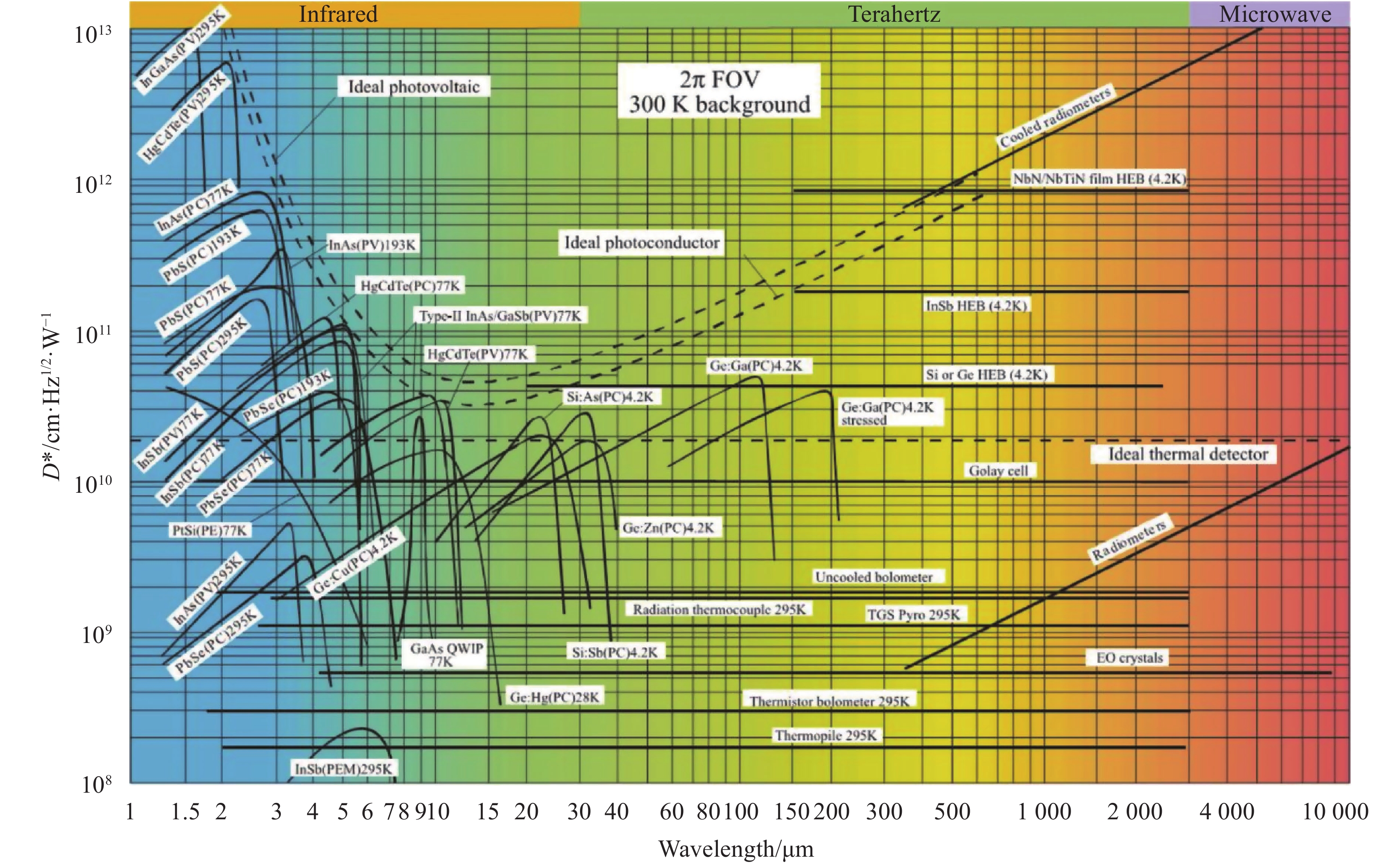
![Comparison of the D* of various available detectors when operated at the indicated temperature and in the region of 1−10 000 μm waveband[4]](/richHtml/irla/2022/51/1/20210988/img_1.jpg)
Fig. 1. Comparison of the D * of various available detectors when operated at the indicated temperature and in the region of 1−10 000 μm waveband[4]
![Hybrid HgCdTe IRFPA detector with independently optimized signal detection and readout. (a) Indium column flip chip interconnection; (b) Loophole interconnection[5]](/richHtml/irla/2022/51/1/20210988/img_2.jpg)
Fig. 2. Hybrid HgCdTe IRFPA detector with independently optimized signal detection and readout. (a) Indium column flip chip interconnection; (b) Loophole interconnection[5]
Fig. 3. Development roadmap and memorabilia for the first generation to the fourth generation of infrared detectors[4]
Fig. 4. H2 RG 2 048×2 048 HgCdTe FPA detector[6]
Fig. 5. 2 048×2 048 HgCdTe FPA used in the Space Telescope Near Infrared Camera[6]
Fig. 6. Quantum efficiency of the H2 RG 2 048×2 048 HgCdTe FPA with 0.8-1.7 μm cutoff which CdZnTe substrate was removed[7]
Fig. 7. Euclid focal plane assembly with 16 H2 RG FPA (2048×2048) (a) and the measured quantum efficiencies (b)[7]
Fig. 8. H4 RG 4 096×4 096 HgCdTe FPA assembly[8]
Fig. 9. (a) Cross-section of Raytheon’s single-mesa dual-band pixel architecture applied to HgCdTe on Si grown by MBE; (b) Scanning electron micrograph of dual-band pixels [9]
Fig. 10. Two-color HgCdTe IR detective structure on GaAs grown by MBE[10]
Fig. 11. Two-color n-p-n HgCdTe IR detective structure on CdZnTe grown by MBE[11]. (a) Side view; (b) Stereoscopic view
Fig. 12. (a) Energy band diagram illustrating the dark current mechanisms for a HgCdTe p-n junction[12]; (b) Energy band diagrams of HgCdTe n+-Bn-n junction[13]
Fig. 13. Calculated detectivity for p-on-n HgCdTe detector plotted versus operating temperature for four important wavelength regions[14]
Fig. 14. Dark current as a function of temperature and cutoff wavelengthfor HgCdTe focal plane detector[7]
Fig. 15. Main specifications of HOT HAWK MWIR focal plane detector operated at 155 K (a) and relationship of temperature with current density (b)[15]
Fig. 16. Relationship between operating temperature and cooling type of HgCdTe focal plane detector in MWIR, LWIR and VLWIR [7]
Fig. 17. Schematic illustration of HgCdTe APDs architecture[16]
Fig. 18. Schematic of the HDVIP structure HgCdTe APD of DRS Company[19-20]. (a) Side view; (b) Top view
Fig. 19. Schematic of HgCdTe APDs by DRS using 2×8 HDVIP p-around-n cylindrical structure. (a) Top view; (b) Side view [18]
Fig. 20. DRS mini-Stirling cryocooler for the 2×8-pixel HgCdTe FPA[18]
Fig. 21. Measurement of the DRS HgCdTe APD responsivity(a) and NEP(b) as a function of the APD bias voltage[18]
| |||||||||||||||||||||||||||||||||||||||||||||||||||||||||||||||||||||||||||||||||||||||||||||||||||||||||||||||||||||||||||||||||||||||||||||||||||||||||||||||||||||||||||||||||||||||||||||||||||
Table 1. Important alloy compositions and physical parameters for Hg1−x Cdx Te
| |||||||||||||||||||||||||||||||||||||||||||||||||||||||||||||||||||||||||||||||||||||||||||||||||||||||||||||||||
Table 2. Comparison of the various methods used to grow HgCdTe, including bulk, LPE, MOCVD, and MBE[5]

Set citation alerts for the article
Please enter your email address


