We introduce a nanoscale photonic platform based on gallium phosphide. Owing to the favorable material properties, peak power intensity levels of are safely reached in a suspended membrane. Consequently, the field enhancement is exploited to a far greater extent to achieve efficient and strong light–matter interaction. As an example, parametric interactions are shown to reach a deeply nonlinear regime, revealing cascaded four-wave mixing leading to comb generation and high-order soliton dynamics.
In the quest for the integration and miniaturization of photonic devices, reproducing the exceptional properties of optical fibers for the propagation of light is challenging. It has now been widely recognized that silicon photonics suffers from serious limitations for handling optical signals with large optical power, as is often the case in microwave photonics or, of course, nonlinear optics [1]. Recently, a variety of materials have been proposed to overcome these limitations: silicon nitride (SiN) and doped glass [2], amorphous silicon [3], diamond [4], and chalcogenides [5]. Each of these platforms comes with very specific advantages: very low losses (SiN and doped glass), excellent thermal properties and transparency (diamond), and a large nonlinear response (chalcogenides and semiconductors).
Crucial in the photonic integration is the availability of materials providing a large index contrast, and hence a strong optical confinement. More than two decades ago, George Stegeman, a pioneer in the field of nonlinear optics, proposed a nonlinear photonic platform optimized for the telecom spectral domain-based III-V semiconductor alloys such as [6]. This choice combines large index contrast with the suppression of two-photon absorption (TPA). Fabrication imperfections, however, and related propagation losses have been an issue for a long time.
Nanoscale photonic structures, such as photonic crystal waveguides, allow the tailoring of the dispersion and achievement of a regime where the group velocity is more than an order of magnitude smaller than that of light in a vacuum [7]. It has been shown that, due to the resulting large increase of the optical intensity, slow light enables a considerable enhancement of nonlinear interactions [8]. The operation of nanoscale waveguides in a deep nonlinear regime is therefore extremely demanding in terms of material properties, since not only the nonlinear absorption has to be minimized, but the thermal properties also must be very good to cope with the effects of the unavoidable residual absorption.
Sign up for Photonics Research TOC. Get the latest issue of Photonics Research delivered right to you!Sign up now
The introduction of ternary alloy lattice matched to GaAs, namely in the context of photonic crystals, has allowed a drastic reduction of the nonlinear absorption. The power flux thus greatly exceeds the level necessary to trigger strong nonlinearities. If the effective Kerr nonlinearity has been increased by seven orders of magnitude compared to single mode fibers [9], the application in the context of optical signal processing is still hampered by the small thermal conductivity of this ternary alloy.
Here we propose a nonlinear nanoscale photonic platform based on the binary semiconductor, gallium phosphide, which can now be grown directly on a silicon substrate. Along with its large thermal conductivity () [10], which is comparable to silicon and about a factor 20 larger than in GaInP, this material also provides a very large transparency window (from 550 nm to infrared wavelengths), owing to the large electronic band gap (2.26 eV) that also minimizes the nonlinear absorption. Its second-order optical nonlinearity, forbidden in centro-symmetric materials such as diamond and silicon, enables a variety of nonlinear parametric processes such as optical sum and difference frequency generation, as demonstrated in photonic crystal cavities, microdisks, and ring resonators [11–13]. This nonlinearity has also been exploited in the context of an integrated photonics platform for quantum information [14,15].
Here we focus on GaP photonic crystal suspended slab waveguides operating at very large average and peak power levels, vastly exceeding any reported level in nanoscale semiconductor membranes. While the observed high-order soliton dynamics leading to the generation of a broad radiation spectra demonstrates the capability to sustain very large optical fields, the parametric amplification at a 2 GHz repetition rate and cascaded four-wave mixing (FWM) down to the 11th harmonic demonstrate the very efficient thermal handling.
2. GALLIUM PHOSPHIDE PHOTONIC CRYSTALS
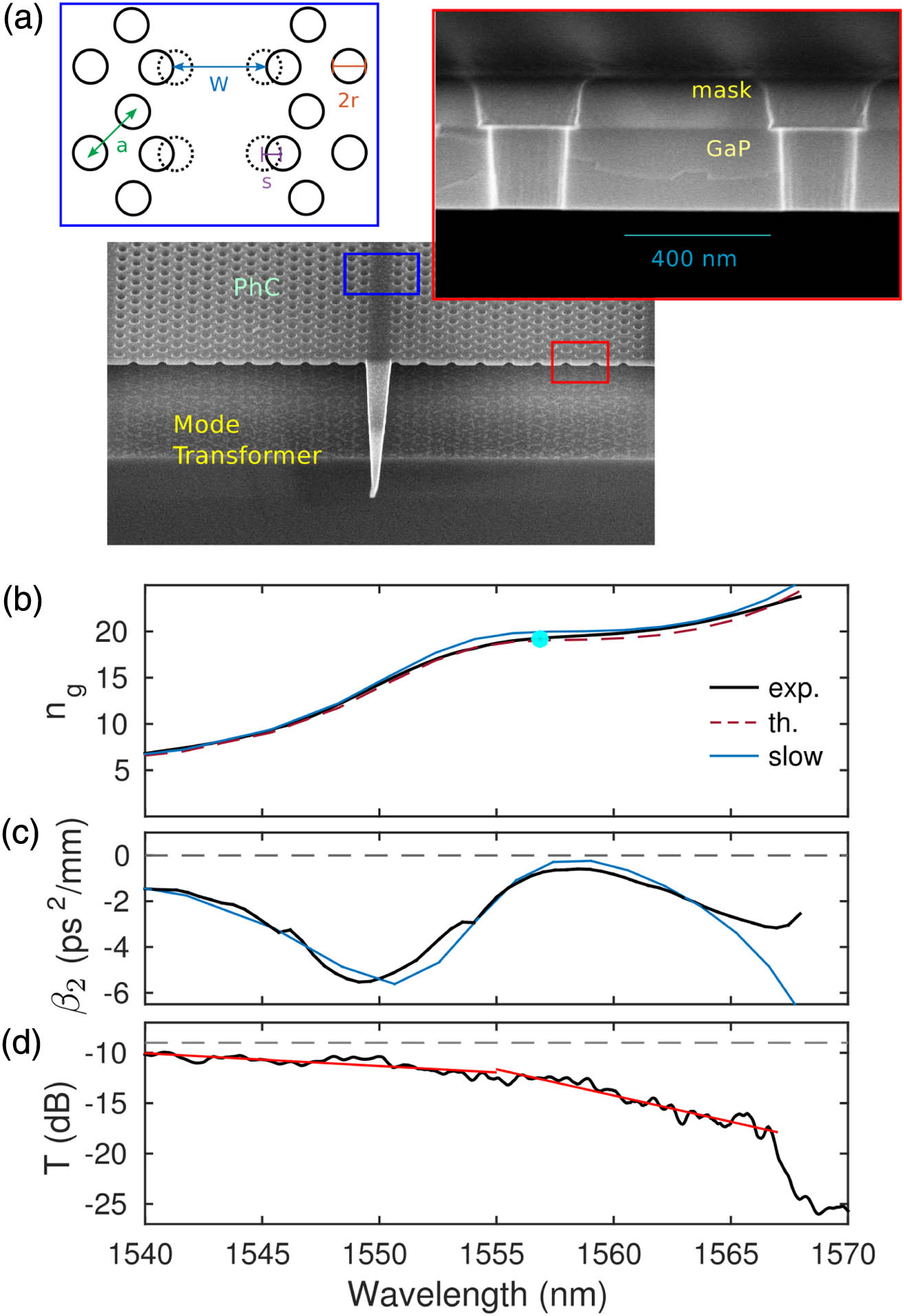
The fabrication of the PhC suspended waveguides sample starts with growth on a GaP substrate of a semiconductor heterostructure by metal–organic chemical vapor deposition (MOCVD) composed of a 230 nm thick GaP layer on top of a 1 μm thick etch stop layer of . The semiconductor slab is patterned with PhC structures using inductively coupled plasma etching (ICP, chemistry based on a HBr, , He gas mix) through a SiN mask. The latter is obtained by depositing SiN on the GaP wafer using plasma-enhanced chemical vapor deposition and structured using electron beam lithography (PMMA ebeam resist) followed by reactive ion etching (, gas mix). Finally, the etch stop layer is selectively chemically etched in buffered HF to suspend the PhC membranes. The result is shown in Fig. 1(a).
Figure 1.(a) SEM image of a PhC waveguide made of a GaP slab and close-up before the removal of the etching mask (red rectangle). The waveguide design (blue rectangle) indicates the relevant parameters, the radius of the holes, ; the period of the triangular lattice, ; the width of the defect line, ; and the transverse shift of the first row of holes, . (b) Calculated (dashed) and measured (solid thick) average group index. The thin blue solid line is the calculated group index in the slow section. The cyan circle corresponds to the FWM experiment (). (c) Corresponding second-order dispersion (same codes). (d) Transmission spectrum, including fiber-to-waveguide coupling (dashed line represents insertion losses). The red lines are a guide for the eyes.
Photonic crystal waveguides are designed to offer an engineered dispersion profile. Following established design rules [16], a triangular lattice (period ) of holes with a line defect (so called “W1”, which stands for the width of the defect line, ) is modified so that the first row of holes is displaced outward by . A schematic top view of the photonic crystal waveguide presents these parameters [Fig. 1(a)]. The devices comprise a dispersion-engineered central section with lengths , 0.8, and 1.2 mm. PhC waveguides with a red-shifted dispersion have been added to connect to the cleaved edge of the chip () where adiabatic spike couplers [Fig. 1(a)] allow low-loss coupling to lensed fibers [17]. The connecting waveguides, so-called “fast-light” sections in the following, are larger, and , and present a reduced group index . A tapered section and is added in between to promote the adiabatic conversion of the mode and prevent unwanted reflections. Each waveguide is fabricated with a single hole size. The radius is, however, changed from waveguide to waveguide to compensate for fabrication tolerances and tune the dispersion properties to the desired ones.
The dispersion of the waveguides is measured using an interferometric technique reminiscent of optical coherent tomography (OCT), but adapted to photonic waveguides [18,19]. This provides the propagation delay through the waveguide as a function of the optical frequency, and the corresponding spatially averaged group index is shown in Fig. 1(b). A comparison with the calculated dispersion reveals that the holes are slightly smaller () than their nominal value (). To extract the dispersion of the “slow-light” section of the waveguide, the calculated contributions from the other sections must be accounted for. Figure 1(c) reveals a very good agreement with the designed dispersion and demonstrates good control of the geometry. To simplify the nonlinear modeling, it is assumed that the contribution of the “fast-light” sections can be accounted for by considering a slightly longer “effective” length of the “slow-light” section.
The propagation losses, , are inferred from the transmission measurement () and fiber-to-waveguide coupling measurements . The propagation losses are estimated assuming that the coupling losses are per facet through with the length of the slow section of the waveguide. The estimate of is based on previous experiments obtained with identical taper design [17]. Hence, the waveguides considered here exhibit propagation losses, for a group index . Thus, from the linear losses standpoint, dominated by the fabrication disorder, the result is almost comparable to other PhC technologies (see Table 1).
Geom. Mat. Exp. Refs.
PhC GaInP Membr. FWM [20]
Sol [21]
PhC GaInP on SiO2FWM [22]
PhC GaP Membr. [This Work]
PhC Si on SiO2FWM [23]
FWM (Sol) [24]
Wire α-Sion SiO2Sol [3]
FWM [25]
Wire AlGaAs on SiO2FWM [26]
FWM
Sol
Δt
ps
30
2
CW
4
15
CW
CW (1)
1.8
3.8
CW
ζ
%
0.5
0.007
100
3
0.015
100
100 (0.002)
0.004
100
P
W
0.8
10
4.5
20†
(30)
5.3
1.5
P¯
mW
4
0.8
100
135
1.7
90
20 (0.6)
3
0.2
1.5
I
GW/cm2
≈10
12
50†
≈30
4
≈5
≈0.75
I¯
MW/cm2
≈10
≈600
400
≈600
20
≪1
≈750
Aeff
μm2
≈0.03
0.04
0.04
≈0.03
≈0.1
<0.1
<0.1
≈0.2
Aχ(3)
μm2
0.004
0.02
0.006
0.01
0.015
0.006
0.21
0.07
0.07
0.14
ng
15
9
30
20
15
30
3.5
3.5
3.5
3
n2
10−17W−1·m−2
0.7
0.7
0.35
≈0.6
1.7
2.1
1.3
2.5
α
dB/cm
0.1ng2
<0.1ng2
0.16ng2
<0.1ng2
4
4.5
4.8
1.5
η
dB
5
n.a.
−18
0.8
n.a.
−24
−21
n.a.
+26
>0
γ
W−1·m−1
6000
1000
4500
1600
1000
4000
330
1200
770
650
γ/α
W−1
6
1.5
2.5
1.5
1
2.5
4
12
7
>20
F
≫1
≫1
1.5±0.5
0.4 (TE)
5 (TM)
5 (TE)
2 (TE)
≫1
Table 1. Performances of Semiconductor Nanoscale Waveguides (PhC or Wires) in the Telecom C Banda
An ideal material for chip scale nonlinear optics would be described by the nonlinear Schrodinger equation, as is the case for optical fibers, meaning that other effects, in particular nonlinear absorption, but also free carrier effects, are negligible. In semiconductors, this is very challenging, although PhC has so far provided an excellent tradeoff [9]. Indeed, a variety of phenomena have been observed, such as soliton compression [21], fission [27], spectral broadening, pulse acceleration [28], and self-frequency shift [29]. The observation of gap solitons, predicted at even larger levels of nonlinearity [30], remains elusive instead, because of the very high levels of nonlinear response required. The first experiment aims precisely at demonstrating the high peak power-handling capability of GaP photonic nanostructures.
The nonlinear propagation of picosecond pulses generated from a spectrally filtered femtosecond passively mode-locked laser (Optisiv) in the GaP waveguide is described in Fig. 2. At the largest pulse energy (48 pJ) coupled in the waveguide, the pulse undergoes a strong spectral broadening [Fig. 2(b)] and higher order soliton dynamics resulting in the creation of three peaks [Fig. 2(a)]. These measurements are reproduced by a model based on the nonlinear Schrodinger equation, where the dispersion of the “slow” waveguide accounts for exactly [9]. The nonlinear term only contains the Kerr effect (including nonlinear absorption). Free carrier effects are also considered, even though they only induce small corrections. The autocorrelation of the pulse at the output is reproduced by including the propagation in the weakly nonlinear, but strongly dispersive, “fast” sections. The same model reveals the higher-order soliton dynamics [Fig. 2(c)], where a peak power of roughly 22 W is reached when the pulse duration decreases from the initial 4 ps down to 0.7 ps. It is therefore estimated that under these conditions the peak irradiance in the nanostructured GaP reaches the value of about , which is only one order of magnitude below peak levels in high-power optical fibers.
Figure 2.Picosecond pulse propagation and soliton dynamics. (a) Autocorrelation traces, experimental (grey circles) and calculated (red line). (b) Corresponding experimental output (grey circles) and input (cyan line) spectra. The calculated output spectrum (solid red line) is also represented with the calculated input one (dashed black line). (c) Calculated evolution of the pulse at some specified positions inside the waveguide. (d) Evolution of peak power P, pulse energy W, and duration .
In nanostructured materials, surface effects are important and may alter the properties the bulk materials are known for. Therefore, the analysis of the pulse propagation dynamics has been performed to characterize the nonlinear response of GaP nanoscale waveguides. Figure 3 compares different estimates for the nonlinear parameter . A first method is based on the measurement of the nonlinear phase shift through the spectral broadening [31], as shown in Fig. 3(b). It is apparent that this leads to an overestimate, because pulses undergo compression. For the same reason, the extraction of the nonlinear absorption based on the plot of the inverse transmission [Fig. 3(a)] is also affected by a similar issue. An interesting approach is based on the dispersive scan technique that has been successfully implemented on silicon nanoscale waveguides [32]. As performed in earlier research [33], we extract the nonlinear parameters through the full modeling of the propagation. The nonlinear parameter , also representing the nonlinear absorption through its imaginary part, is used as an adjustable parameter for the best fit of the output spectra, autocorrelation, and transmission. The results are compared with the calculated through the nonlinear cross section (see Appendix A), which leads to an estimate of the Kerr coefficient .
Figure 3.(a) Measurement of the nonlinear absorption for through the plot of the inverse transmission versus the peak power in the waveguide. (b) Nonlinear phase shift . (c) Calculated inverse linear and nonlinear cross sections and as a function of the group index (see Appendix A). (d) Nonlinear parameter versus group index. Estimate from the spectral broadening (magenta squares), values used in the model (green circles), and calculated (solid line) using . The dashed red line represents the dependence as a guide for the eyes.
This can be compared with the value of the measurement performed on GaP at 1.06 μm [34]. Namely, using Ref. [35], a scaling factor of for GaP, yields at μ, which is reasonably close to our estimate.
The scaling of the inverse transmission with the peak power [Fig. 3(a)] reveals that the nonlinear absorption is not negligible, in spite of the large electronic band gap (). A possible explanation points to the role of surface defects. Similar to silicon photonic wires, where linear absorption due to defects at the surface is not negligible at all [36], here we speculate that surface defects induce TPA, because of the much larger band gap compared to silicon. The almost symmetric broadening of the spectra confirms that free carrier effects are small. The estimated TPA in the waveguide leads to the conclusion that the nonlinear figure of merit [37,38] is . This is close to the criteria for all-optical switching (), while in silicon the figure of merit is way out of target (), as reported in Ref. [1].
5. PARAMETRIC GAIN AT GHZ RATE
A much lower limit to the power handling is set by thermal effects becoming increasingly important when approaching the continuous wave regime. For instance, parametric gain due to FWM has been demonstrated in GaInP PhC chip [20]; however, thermal issues forced operation at a low repetition rate (156 MHz). In communication and optical processing, a far higher rate is necessary, which implies a larger average power density. The FWM conversion efficiency has been probed with a pulsed pump (duration 15 ps, peak coupled power ) from a mode-locked fiber laser (Pritel) and a continuous-wave (CW) probe with detuning spanning over the phase-matching domain of the parametric interaction. As shown in Fig. 3(a), the pump wavelength is set to 1557 nm, where the group index is and the dispersion is . The nonlinear coefficient is about , which is calculated using , consistently with the other measurements. This corresponds to an optimum for the conversion efficiency, which depends on the particular dispersion profile.
The figure of merit for this process, the conversion efficiency, is defined as the integrated spectral power of the idler divided by the input signal power. An estimate for it is , extracted from the output spectra by accounting for the filling factor (as in Ref. [20]) and having calibrated the optical spectrum analyzer (OSA) reading for CW and pulsed signals. The filling factor corresponds to , with , the pulse duration and , the repetition rate. The conversion efficiency spectra for varying frequencies of the probe and increasing pump powers are plotted in Fig. 4(b). The bandwidth of the FWM process for this wavelength of the pump is . Indeed, the enhanced nonlinearity in PhC waveguide also comes with a limited bandwidth of operation, which constitutes a major difference with wire waveguides. The on-chip maximal conversion efficiency of is obtained for a coupled pump power of 4.4 W and a pump-probe detuning of 2 nm.
Figure 4.Four-wave mixing experiment with ps pulses at 2 GHz rate. (a) Output spectra corresponding to two different coupled peak power levels and spectrum of the pump at input. (b) Measured conversion efficiency as a function of the pump-probe detuning as the pump power is increased. The colored solid lines stand for the theory. The peak conversion efficiency is plotted versus the pump power in the inset and compared with the model (solid lines), which also provides the parametric gain . Filled circles correspond to the plots according to the color code.
Figure 5.Cascaded four-wave mixing experiment with ns pulses. (a) Output spectra and (b) raw conversion efficiency () as a function of the peak power. The dashed line corresponds to . Detail of (c) the output and (d) the input at maximum peak power: experimental (red) and calculated (black) spectra.
Very interestingly, a maximum at a nonzero detuning is observed. This is the signature of the nonlinear phase shift due to cross-phase modulation (XPM) and self-phase modulation (SPM) compensating for the linear mismatch, which only happens when a deep NL regime is reached and when all the other effects (e.g., nonlinear losses and carrier effects) are negligible. The output spectrum at this power is shown in the inset of Fig. 4, and the CW probe and the pump show the distinctive spectral widening and deformation of self-phase modulation. This behavior suggests that off-chip gain was achieved. The conversion efficiency is properly defined as and can be estimated from by subtracting the propagation losses; hence, . Thus, the off-chip gain is . As shown in the inset of Fig. 3(b), the agreement of the conversion efficiency with the model is very good, demonstrating that up to reaching gain (), the nonlinear waveguide is operating as predicted by simple FWM theory.
When estimating the peak and time-averaged irradiance at maximum gain, we obtain and , respectively. In terms of fluence, this translates to about . These values correspond to a coupled average power that is about 130 mW. Because thermal sinking is very efficient, the material still behaves as an almost ideal Kerr material, in spite of such high power levels.
6. NONRESONANT COMB GENERATION
Finally, we address a regime with longer (5 ns) pump and signal pulses, generated from two CW lasers modulated using a pattern generator and two Mach–Zehnder modulators. After amplification, the average (peak) power injected in the waveguide is about 14 mW (1.1 W). The waveguide has the same design as in Fig. 1, except that its dispersion is blue-shifted by about 11 nm. It is operated near zero dispersion and large group index. More precisely, , and . High-resolution optical spectra (Yenista OSA 20) are recorded as a function of the input power, keeping the pump to signal ratio constant. As apparent in Fig. 5, at the maximum power level the on-chip conversion efficiency is . Note that the quadratic scaling of with the peak power is followed up to the maximum power, where the process saturates, because the signal and idler are only a few dB below the pump. Because of the very small detuning (14.8 GHz), up to 11 ancillary idlers are within the FWM bandwidth and are therefore generated in a cascaded process as the pump power increases. The agreement with the generalized NLSE model is fairly good with , which was also calculated as in the previous sections. Under this condition, the maximum irradiance is , but the fluence reaches because of the much longer pulses. This last result demonstrates the capability of the suspended GaP membrane to sustain large powers for several nanoseconds, which enables the formation of a comb of spectrally narrow lines. We also point out that because this cascaded FWM process is not resonant, the spacing of the comb can be adjusted by controlling the detuning of the two inputs.
7. CONCLUSION
Owing to the combination of a large refractive index and advanced nanofabrication techniques, photonic structures are now able to concentrate the optical field so tightly that very large optical intensities are achieved. As a consequence, the light–matter interactions, particularly nonlinear phenomena, are so much enhanced that they can effectively be exploited for fundamental science as well as for applications such as optical signal processing. However, undesirable effects also appear at such large levels of power intensities. The severity of these effects is strongly related to the material.
We have developed the technology for nanoscale photonics based on gallium phosphide. The combination of large thermal conductivity, a good nonlinear figure of merit (reduced nonlinear absorption), and a still large nonlinear response compared to non-semiconductor materials makes it particularly suited for nonlinear photonics on a chip. Table 1 summarizes recent achievements with nanoscale waveguides. We focus on soliton propagation and FWM, because they are representative of the challenges inherent in on-chip nonlinear optics. GaP is thereby compared with GaInP [20–22] and silicon [23]. The comparison is extended to more conventional wire waveguides made of amorphous silicon [24]. We note that silicon oxynitride is also being developed for photonic nanostructures [39].
First of all, soliton dynamics and compression lead to extremely large intensities, ultimately limited by the nonlinear figure of merit and the thermal conductivity. Here, GaP is superior to GaInP and both are superior to silicon, which is apparent when comparing the maximum irradiance in the table. Similarly, net parametric gain can only be achieved when the nonlinear phase shift is large enough, which explains why gain is reached with III-V materials or in amorphous silicon [25], although in a pulsed regime. The notable exception is AlGaAs wires on silica [26], which are able to sustain a CW irradiance of , which is large enough to allow parametric gain.
Achieving large nonlinearities in CW is, however, very challenging on a suspended membrane. In this respect, GaP nanoscale waveguides have allowed a 30-fold increase of the average power over GaInP. This led to the achievement of parametric gain at a GHz rate, which is relevant to all-optical signal processing. We note that the time-averaged irradiance in GaP suspended membranes is comparable to what has been reported in waveguides embedded in a solid cladding [22,23,26].
This result is important because suspended semiconductor membranes allow the full exploitation of the large contrast of the dielectric permittivity () to create robust high-Q and low mode volume cavities. This is a key asset for enhanced light–matter interaction and also optomechanics. Moreover, a large power handling capability is important in the context of microwave photonics.
Acknowledgment
Acknowledgment. A. Martin acknowledges financial support from IDEX AAP IDI 2013.
APPENDIX A: LINEAR AND NONLINEAR CROSS SECTIONS
In the context of the coupled mode theory, effective cross sections are used to connect the spatially distributed linear and nonlinear interaction occurring in nonhomogeneous media to the total power propagating through it. This defines the normalization . Consequently, the nonlinear coefficient is calculated as an integral of the normal mode
Here, is the ratio between the spatial distribution of the nonlinear tensor to a reference value. If the nonlinear material is homogeneous and is defined in a subvolume , then in this volume and vanishes outside. The effective area for the process is related to through the definition
The effective area relates the power flowing in the waveguide to the spatial maximum of the field, and more precisely of the irradiance . This defines , where the mode is normalized to carry unitary power (). Note that here is the refractive index of the homogeneous material and is the spatial distribution of the relative permittivity. This area is much smaller than the mode area defined as , the difference being that here the slow light enhancement is not taken into account. The nonlinear parameter is instead related to the Kerr coefficient of the material through the definition and the area , which is given in Ref. [9].
[38] To conform to recent literature, we use the current definition of the NL FOM, which is related by F=2/T to T=(2πn2)/(λα2)>1 the original definition.