• Acta Physica Sinica
  • Vol. 69, Issue 9, 096801-1 (2020)
Hao-Chang Lü1、2, Yun-Chi Zhao2, Guang Yang1, Bo-Wen Dong1, Jie Qi1, Jing-Yan Zhang1, Zhao-Zhao Zhu2, Yang Sun2, Guang-Hua Yu1, Yong Jiang1, Hong-Xiang Wei2, Jing Wang2, Jun Lu2, Zhi-Hong Wang2, Jian-Wang Cai2, Bao-Gen Shen1、2, Feng Yang3, Shen-Jin Zhang3, and Shou-Guo Wang1、2、*
Author Affiliations
  • 1Department of Materials Physics and Chemistry, School of Materials Science and Engineering, University of Science and Technology Beijing, Beijing 100083, China
  • 2State Key Laboratory of Magnetism, Institute of Physics, Chinese Academy of Sciences, Beijing 100190, China
  • 3Key Laboratory of Functional Crystals and Laser Technology, Technical Institute of Physics and Chemistry, Chinese Academy of Sciences, Beijing 100190, China
  • show less
    DOI: 10.7498/aps.69.20200083 Cite this Article
    Hao-Chang Lü, Yun-Chi Zhao, Guang Yang, Bo-Wen Dong, Jie Qi, Jing-Yan Zhang, Zhao-Zhao Zhu, Yang Sun, Guang-Hua Yu, Yong Jiang, Hong-Xiang Wei, Jing Wang, Jun Lu, Zhi-Hong Wang, Jian-Wang Cai, Bao-Gen Shen, Feng Yang, Shen-Jin Zhang, Shou-Guo Wang. High resolution imaging based on photo-emission electron microscopy excited by deep ultraviolet laser[J]. Acta Physica Sinica, 2020, 69(9): 096801-1 Copy Citation Text show less
    Schematic drawings of the DUV laser optical system with (a) circular and (b) linear polarizations[69].
    Fig. 1. Schematic drawings of the DUV laser optical system with (a) circular and (b) linear polarizations[69].
    Optical system of the DUV-PEEM system.
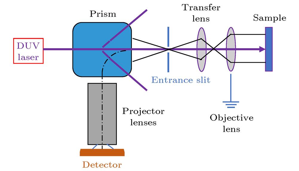
    Fig. 2. Optical system of the DUV-PEEM system.
    A schematic layout of the DUV laser-based LEEM/PEEM system[69].
    Fig. 3. A schematic layout of the DUV laser-based LEEM/PEEM system[69].
    Schematic setup and photo of MBE-PEEM combined system.
    Fig. 4. Schematic setup and photo of MBE-PEEM combined system.
    (a) PEEM image of multilayer graphene on Ru (0001) taken with Hg arc lamp; (b) spatial resolution calculated from obtained PEEM image[71].
    Fig. 5. (a) PEEM image of multilayer graphene on Ru (0001) taken with Hg arc lamp; (b) spatial resolution calculated from obtained PEEM image[71].
    Optical system of LEEM (E-Gun).
    Fig. 6. Optical system of LEEM (E-Gun).
    (a) Dark field image and (b) LEED pattern of a (2 × 1) reconstructed Si (001) surface; (c) spatial resolution calculated from obtained LEEM image[71].
    Fig. 7. (a) Dark field image and (b) LEED pattern of a (2 × 1) reconstructed Si (001) surface; (c) spatial resolution calculated from obtained LEEM image[71].
    (a) DUV-PEEM image of PbO islands on Ru(0001); (b) spatial resolution calculated from obtained PEEM image[71].
    Fig. 8. (a) DUV-PEEM image of PbO islands on Ru(0001); (b) spatial resolution calculated from obtained PEEM image[71].
    (a) Schematic drawing of energy filter in PEEM system; (b) DUV-photo emission spectrum obtained from island-shaped PbO grown on Ru (0001) in dispersion mode; (c) normalized line profile with the calculated spatial resolution from selected area marked in panel (b).
    Fig. 9. (a) Schematic drawing of energy filter in PEEM system; (b) DUV-photo emission spectrum obtained from island-shaped PbO grown on Ru (0001) in dispersion mode; (c) normalized line profile with the calculated spatial resolution from selected area marked in panel (b).
    (a) Schematic structure and out-of-plane hysteresis loop of MgO (001) sub. /Cr (5 nm)/Pt (10 nm)/FePt (20 nm) films; (b) LEEM image (Ep = 8.6 eV) and LEED (Ep = 16.3 eV) pattern (inset) of FePt film; (c) magnetic domain (contrast enhanced) of the area marked by a red dashed rectangle in (b) taken with circularly polarized DUV laser; (d) magnetic domain image of the FePt films with the same structure obtained by magnetic force microscopy; (e) normalized line profile with the estimated spatial resolution from selected area marked in inset[69].
    Fig. 10. (a) Schematic structure and out-of-plane hysteresis loop of MgO (001) sub. /Cr (5 nm)/Pt (10 nm)/FePt (20 nm) films; (b) LEEM image (Ep = 8.6 eV) and LEED (Ep = 16.3 eV) pattern (inset) of FePt film; (c) magnetic domain (contrast enhanced) of the area marked by a red dashed rectangle in (b) taken with circularly polarized DUV laser; (d) magnetic domain image of the FePt films with the same structure obtained by magnetic force microscopy; (e) normalized line profile with the estimated spatial resolution from selected area marked in inset[69].
    (a) Schematic drawing of a Pt seed layer with Cr step. (b) UV PEEM image of Pt seed layer consisting of two orientations. LEEM and LEED patterns of the selected areas marked by blue rectangles in panel (b): (c) dark area A, (d) light area B and (e) boundary area C. (f) DUV-PEEM image of the selected area marked by a red dashed rectangle in panel (b). (g) Linear dichroism image of the same area as panel (f)[69].
    Fig. 11. (a) Schematic drawing of a Pt seed layer with Cr step. (b) UV PEEM image of Pt seed layer consisting of two orientations. LEEM and LEED patterns of the selected areas marked by blue rectangles in panel (b): (c) dark area A, (d) light area B and (e) boundary area C. (f) DUV-PEEM image of the selected area marked by a red dashed rectangle in panel (b). (g) Linear dichroism image of the same area as panel (f)[69].
    (a) UV-PEEM image of FePt film deposited on Pt seed layer with two orientations. LEED patterns of selected areas marked by blue rectangles in panel (a): (b) light area I and (c) dark area II. (d) DUV-PEEM image of the selected area marked by a red dashed rectangle in panel (a) taken with linearly polarized laser[69].
    Fig. 12. (a) UV-PEEM image of FePt film deposited on Pt seed layer with two orientations. LEED patterns of selected areas marked by blue rectangles in panel (a): (b) light area I and (c) dark area II. (d) DUV-PEEM image of the selected area marked by a red dashed rectangle in panel (a) taken with linearly polarized laser[69].
    DUV-PEEM images taken with (a) left-circularly polarized and (b) right-circularly polarized light; (c) MCD image of FePt film; (d), (e) DUV-PEEM images taken with linearly-polarized laser (polarization shown by red arrow); (f) MLD image of FePt film; (g) polarization dependent MLD asymmetry for the selected area[69].
    Fig. 13. DUV-PEEM images taken with (a) left-circularly polarized and (b) right-circularly polarized light; (c) MCD image of FePt film; (d), (e) DUV-PEEM images taken with linearly-polarized laser (polarization shown by red arrow); (f) MLD image of FePt film; (g) polarization dependent MLD asymmetry for the selected area[69].
    Source
    DUV-DPLSynchrotron radiationGas discharge laser
    Energy resolution/meV~0.261—5~1.2
    Photon circulation1014—10151010—1012~1012
    Photon flux density/photon·s–1·cm–21019—10201012—1014< 1014
    Wavelength range/nm170—2101—21058.5
    Mode of operationns, ps, fs pulseps pulsecontinuous wave
    Detection depth/nm~10 (bulk effect)0.5—2 (skin effect)~0.5 (skin effect)
    Table 1.

    Properties comparing of the three source[65].

    三种光源的特性比较[65]

    Hao-Chang Lü, Yun-Chi Zhao, Guang Yang, Bo-Wen Dong, Jie Qi, Jing-Yan Zhang, Zhao-Zhao Zhu, Yang Sun, Guang-Hua Yu, Yong Jiang, Hong-Xiang Wei, Jing Wang, Jun Lu, Zhi-Hong Wang, Jian-Wang Cai, Bao-Gen Shen, Feng Yang, Shen-Jin Zhang, Shou-Guo Wang. High resolution imaging based on photo-emission electron microscopy excited by deep ultraviolet laser[J]. Acta Physica Sinica, 2020, 69(9): 096801-1
    Download Citation