Abstract
In this work, a two-step metal organic chemical vapor deposition (MOCVD) method was applied for growing β-Ga2O3 film on c-plane sapphire. Optimized buffer layer growth temperature (TB) was found at 700 °C and the β-Ga2O3 film with full width at half maximum (FWHM) of 0.66° was achieved. A metal?semiconductor?metal (MSM) solar-blind photodetector (PD) was fabricated based on the β-Ga2O3 film. Ultrahigh responsivity of 1422 A/W @ 254 nm and photo-to-dark current ratio (PDCR) of 106 at 10 V bias were obtained. The detectivity of 2.5 × 10¹⁵ Jones proved that the photodetector has outstanding performance in detecting weak signals. Moreover, the photodetector exhibited superior wavelength selectivity with rejection ratio (R250 nm/R400 nm) of 105. These results indicate that the two-step method is a promising approach for preparation of high-quality β-Ga2O3 films for high-performance solar-blind photodetectors.Introductions
As an emerging wide band gap semiconductor material, β-Ga2O3 is considered as one of the most promising materials for power-electronic devices and solar-blind detectors. It is benefit from the excellent material properties of β-Ga2O3 including ultrawide bandgap (4.6−5.2 eV), high critical field (8 MV/cm), high Baliga’s figure-of merit (3214) and good chemical stability[1−3]. β-Ga2O3 solar-blind ultraviolet (200−280 nm) photodetectors have wide application owing to their superiorities, such as low background noise, high response value and radioresistance[4, 5]. In order to improve the photodetector performance, a series of methods are conducted to grow β-Ga2O3 films, including molecular beam epitaxy (MBE)[6], halide vapor phase epitaxy (HVPE)[7], low pressure chemical vapor deposition (LPCVD)[8, 9], mist chemical vapor deposition (mist CVD)[10] and MOCVD[11]. Metal−semiconductor−metal (MSM) structure has the advantages of simple fabrication process, convenient integration with readout circuits and high responsivity because of internal gain. Pratiyush et al.[12] demonstrated MSM detector using heteroepitaxial β-Ga2O3 films with a high responsivity of 1.5 A/W. Qian et al.[13] reported MSM detector based on amorphous Ga2O3 films with an ultrahigh response of 70.26 A/W and specific detection rate of 1.26 × 10¹⁴ Jones. By growing polycrystalline β-Ga2O3 film, Arora et al.[14] had prepared the high-performance MSM detector with a response of 96.13 A/W.
Although β-Ga2O3 film grown by various technologies have been reported, there are still some difficulties in getting ideal quality β-Ga2O3 films. For example, the expensive substrate for homoepitaxial and the large lattice mismatch for heteroepitaxial. As low-cost substrates, sapphires are widely used in heteroepitaxial β-Ga2O3 films. However, the lattice mismatch between c-sapphire and β-Ga2O3 is 3.5%. The stress caused by lattice mismatch will lead to a high dislocation density, which is not conducive to the epitaxial growth of material. In order to alleviate lattice mismatch and improve crystalline quality of epitaxial films, a buffer layer between substrate and epitaxial layer can be applied. However, there are few reports about the effect of buffer layer on the quality of β-Ga2O3 film on c-sapphire[15, 16].
In this work, high-quality β-Ga2O3 films were grown by two-step MOCVD method on c-sapphire. By varying buffer layer growth temperature, β-Ga2O3 film with fullwidth at half maximum (FWHM) of 0.66° was obtained. The MSM solar-blind photodetector was fabricated to further verify the excellent performance of β-Ga2O3 film quality. The solar-blind photodetector exhibits high responsivity of 1422 A/W @ 254 nm. In addition, ultrahigh PDCR (106), detectivity (2.5 × 10¹⁵ Jones) and respond speed (36 ms) were also achieved from the fabricated photodetector. This work provides an approach for the preparation of high-quality β-Ga2O3 films and the application of β-Ga2O3 solar-blind photodetectors.
Experimental details
Four β-Ga2O3 samples were prepared by depositing on c-plane (0001) sapphire in a MOCVD system by the two-step method. First, the thin buffer layer of Ga2O3 was deposited at low temperature (TB), and then β-Ga2O3 film was grown on the buffer layer at 960 °C. Trimethylgallium (TMG) and O2 were used as gallium and oxygen precursors, respectively. High-purity argon was used as carrier gas for TMG source. Four β-Ga2O3 films samples were grown at the same condition, except that TB were at 650, 700, 750 and 800 °C. The crystalline quality of β-Ga2O3 films were characterized by high-resolution X-ray diffraction (HRXRD, X’Pert3 MRD). The surface morphologies of films were investigated by atomic force microscopy (AFM, SII Nanonavi) and scanning electron microscope (SEM, NanoSEM650). The photodetector with MSM structure was fabricated on the β-Ga2O3 film with TB = 700 °C. Si ion implantation process[17, 18] was performed and followed by deposition of Ti/Au electrode. After lift-off process, the interdigital electrodes were formed and the rapid thermal annealing at 475 °C for 1 min was conducted. The room-temperature optical responsivities of β-Ga2O3 PD were measured by an Agilent B1500A semiconductor parameter analyzer and ultraviolet light emitting diodes (UV LEDs) emitting 254 and 356 nm light. Spectral-response measurements at −1 V bias were performed by spectrometer equipped with Xe light source. An Si detector was tested for calibrating the spectrum response.
Results and discussion
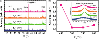
The crystal property of β-Ga2O3 films was measured by XRD with ω−2θ scan mode. Fig. 1(a) shows the XRD spectra of Ga2O3 films with varying TB from 650 to 800 °C. Three diffraction peaks at 18.9°, 38.3°, and 58.9° exhibit well-defined (−201), (−402), and (−603) planes of β-Ga2O3, respectively, indicating the (−201) oriented single crystal growth. This is owing to the similar oxygen atomic arrangement of (−201) plane β-Ga2O3 and c-sapphire. The diffraction peak intensity of β-Ga2O3 film with TB = 650 °C is weak, which is likely due to the low migration rate of adsorbed atoms on substrate surface at low growth temperature. When increasing TB, the crystalline quality of epitaxial layer is improved and the intensity of diffraction peak increases. Figs. 1(b) gives the ω scanning diffraction pattern of (−402) β-Ga2O3 planes and the FWHM values at different TB. The FWHM values of films prepared at different TB of 650, 700, 750, and 800 °C are 3.3°, 0.66°, 0.67°, and 0.93°, respectively. The β-Ga2O3 films in this work grown by two-step method have much lower FWHM values, compared with previously reported β-Ga2O3 films on sapphire[19−21]. The sample grown at TB = 700 °C shows the lowest FWHM value, indicating the optimized buffer layer growth condition is found.

Figure 1.(Color online) (a) XRD ω−2θ scan and (b) FWHM of rocking curve for β-Ga2O3 films grown at different TB. Inset shows the XRD ω scan for films.
AFM was performed to further investigate the surface morphology of films deposited on c-sapphire with different TB. In Fig. 2(a), four samples were examined by AFM scan on a 5 × 5 μm scan area. The surfaces of four samples all show regular pseudo-hexagon structures, which are generated by the in-plane rotational domains and attributed to the symmetries of c-sapphire and β-Ga2O3[22, 23]. The film with TB = 650 °C presents the sparsest texture, which is owing to the low mobility of crystal nuclei during the initial growth and lead to sparse grains difficult to merge. The sample with TB = 700 °C exhibits the densest texture, which is likely attributed to the moderate crystal nuclei mobility at this temperature. As the temperature rises (with TB = 750 or 800 °C), the atom mobility increases, leading to the deposition of large crystal nuclei on substrates and resulting in rough surfaces. Fig. 2(b) shows the surface roughness of four samples, which are 19, 6.8, 7.5, and 12 nm, respectively. Fig. 2(c) gives the variation in film thickness with different TB and inset shows the cross-sectional SEM image of sample grown with TB = 700 °C. The thickest β-Ga2O3 film of 1 μm is obtained when TB = 700 °C. These results indicate that the buffer layer temperature at 700 °C is favorable for β-Ga2O3 film two-step growth.
Figure 2.(Color online) (a) AFM images and (b) RMS roughness of β-Ga2O3 films, (c) film thicknesses obtained from the cross-sectional SEM. Inset shows the cross-sectional image of film grown at TB = 700 °C.
The MSM solar-blind photodetector was fabricated on β-Ga2O3 film with TB = 700 °C. Fig. 3(a) shows the optical microscope diagram of device. Fig. 3(b) reveals the three-dimensional structure diagram of the device. Fig. 3(c) shows the I−V characteristic curve of MSM photodetector. As revealed in figure, the dark current is 400 pA at 10 V bias. Moreover, the I−V curve increases only a little under 365 nm light (light intensity of 15 mW/cm2), indicating that β-Ga2O3 film is not sensitive to 365 nm light. However, the I−V curve increases steeply under 254 nm light (light intensity of 1.9 mW/cm2), suggesting strong light response characteristics and excellent solar-blind photoelectric characteristics.
Figure 3.(Color online) (a) The optical microscope diagram and (b) structural diagram of MSM photodetector. (c) The I−V characteristics of the MSM photodetector in the dark and illuminated by 254 and 365 nm. (d) The energy band diagram and photogenerated carriers of MSM β-Ga2O3 detector with external bias under 254 nm illumination.
The light/dark current rejection ratio (PDCR)[24], which is defined as (Iphoto − Idark )/Idark, achieves an extremely large value of more than 106, indicating that the device has extremely high sensitivity. The responsivity of MSM detector with effective illumination area about 4.55 × 104μm2 reaches 1422 A/W under 10 V bias. Detectivity (D*) can be used to evaluate the ability to perceive the lowest detectable signal, which is related to background noise. Assuming that dark current is the main source of device noise, D* can be expressed as: RS1/2/(2qIdark)1/2 [24]. The photodetection based on high-quality β-Ga2O3 film has a D* of 2.5 × 10¹⁵ Jones under 254 nm light, indicating the ultra-high signal-to-noise ratio. The excellent wavelength selectivity and ultrahigh D* indicate that high sensitivity solar-blind detector is achieved.
Fig. 3(d) is energy band diagram and photogenerated carriers of the fabricated MSM photodetector under 254 nm light with external bias. It is determined from carrier transport mechanism that the optical response of photodetector is a complex process. Photogenerated carriers will be captured by deep-level defects so the lifetime is longer than transmission time. Moreover, electrons are quickly swept-out and reinjected to remain electric neutrality, generating multiple electrons and huge photoconductive gain.
The transient response of MSM photodetector under 254 nm wavelength illumination was tested by controlling the turning on and off for the light source, as shown in Fig. 4(a). When the light source is turned off, the current of the device decays quickly, showing a fast decay speed. In order to quantitatively analyze the response process of current rise and fall, the time responding characteristics are amplified as shown in Fig. 4(b). Then the double exponential relaxation equation is used to fit the I−T curve, and the equation is as follows[25]: I = I0 + Aexp(−t/τ1) + Bexp(−t/τ2), where I0 is the photocurrent in the stable state, t is the time, A and B are constants, τ1 and τ2 denote two relaxation time constants. τ1 reflects the rapid change of carrier concentration after the light source is turned on or off, and τ2 is caused by carrier capture/release due to defects in β-Ga2O3 film. By fitting the photoelectric response curve, the time constants of rising edge are τr1 = 35 ms and τr2 = 181 ms. The decay time constants of falling edge (i.e. the decay time) are: τd1 = 4 ms and τd2 = 32 ms. These values are faster than Ga2O3 photodetectors reported before[24, 26−29]. Furthermore, such fast decay speed (τd = 36 ms) indicates weak persistent photoconductivity (PPC) behavior, which can be caused by the reduced defect density in two-step growth film[29].
Figure 4.(Color online) (a) The time-dependent photoresponse of the Ga2O3 photodetector with external bias to 254 nm illumination, (b) the experimental data and the fitting curve of rise and decay process.
Fig. 5(a) shows the spectral response of the β-Ga2O3 MSM photodetector @−1 V and the peak wavelength is located at ~250 nm (4.97 eV), which is close to the bandgap of β-Ga2O3. The increased responsivity after 400 nm wavelength may be due to the absorption corresponding to the defect energy level. The rejection ratio (R250 nm/R400 nm) of 105 shows a higher response wavelength selectivity than previously reported results[30, 31]. Excellent solar-blind ultraviolet detection characteristic demonstrates the high-quality film and strong interband excited transitions. Fig. 5(b) gives the responsivities and detectivities of the reported deep ultraviolet photodetectors based on Ga2O3 films. It showed clearly that the obtained solar-blind photodetector displays the better comprehensive performance. In addition, the actual responsivity (Ractual) is given by Ractual = GRideal = G(ηq/hν)[6], where η is EQE and ideal responsivity (Rideal) is β-Ga2O3 photodetector detected at 254 nm. Assuming η is 100% and Rideal is 0.2 A/W, the gain (G) is equal to 7110 indicating huge internal gain in β-Ga2O3 photodetector.
Figure 5.(Color online) (a) The photocurrent spectrum of β-Ga2O3 MSM detector at −1 V bias in semilog scale, (b) the responsivity vs detectivity of different solar-blind photodetectors[32−41].
Conclusion
In summary, a Ga2O3 buffer layer is introduced to reduce lattice-mismatch-related defects using MOCVD method. It is found that TB will obviously affect crystalline quality and the optimized buffer layer temperature for two step method is 700 °C. The MSM solar-blind photodetector shows ultrahigh responsivity of 1422 A/W and superior detectivity of 2.5× 10¹⁵ Jones. Besides, a notable rejection ratio (R250 nm/R400 nm) of 105 is realized, indicating the excellent wavelength selectivity. A remarkable gain of 7110 further demonstrates high internal gain in the β-Ga2O3 MSM photodetector. The outstanding photodetector performance suggests that two-step growth method has great potential for preparing high-quality β-Ga2O3 film on sapphire.
References
[1] B Fu, G Z Jian, W X Mu et al. Crystal growth and design of Sn-doped β-Ga2O3: Morphology, defect and property studies of cylindrical crystal by EFG. J Alloys Compd, 896, 162830(2022).
[2] H D Sun, K H Li, C G Torres Castanedo et al. HCl flow-induced phase change of α-, β-, and ε-Ga2O3 films grown by MOCVD. Cryst Growth Des, 18, 2370(2018).
[3] J C Zhang, P F Dong, K Dang et al. Ultra-wide bandgap semiconductor Ga2O3 power diodes. Nat Commun, 13, 3900(2022).
[4] H Sheoran, S Fang, F Z Liang et al. High performance of zero-power-consumption MOCVD-grown β-Ga2O3-based solar-blind photodetectors with ultralow dark current and high-temperature functionalities. ACS Appl Mater Interfaces, 14, 52096(2022).
[5] X H Hou, X L Zhao, Y Zhang et al. High-performance harsh-environment-resistant GaOX solar-blind photodetectors via defect and doping engineering. Adv Mater, 34, 2106923(2022).
[6] T S Ngo, D D Le, N Q Vuong et al. Systematic investigation of growth and properties of Ga2O3 films on c-plane sapphire substrates prepared by plasma-assisted molecular beam epitaxy. ECS J Solid State Sci Technol, 11, 035008(2022).
[7] H Murakami, K Nomura, K Goto et al. Homoepitaxial growth of β-Ga2O3 layers by halide vapor phase epitaxy. Appl Phys Express, 8, 015503(2015).
[8] S Saha, L Y Meng, Z X Feng et al. Schottky diode characteristics on high-growth rate LPCVD β -Ga2O3 films on (010) and (001) Ga2O3 substrates. Appl Phys Lett, 120, 122106(2022).
[9] S Rafique, L Han, A T Neal et al. Heteroepitaxy of N-type β-Ga2O3 thin films on sapphire substrate by low pressure chemical vapor deposition. Appl Phys Lett, 109, 132103(2016).
[10] Y Xu, Z Y An, L X Zhang et al. Solar blind deep ultraviolet β-Ga2O3 photodetectors grown on sapphire by the Mist-CVD method. Opt Mater Express, 8, 2941(2018).
[11] D Q Hu, S W Zhuang, Z Z Ma et al. Study on the optical properties of β-Ga2O3 films grown by MOCVD. J Mater Sci: Mater Electron, 28, 10997(2017).
[12] S P Anamika, K Sriram, V S Swanand et al. High responsivity in molecular beam epitaxy grown β-Ga2O3 metal semiconductor metal solar blind deep-UV photodetector. Appl Phys Lett, 110, 221107(2017).
[13] L X Qian, Z H Wu, Y Y Zhang et al. Ultrahigh-responsivity, rapid-recovery, solar-blind photodetector based on highly nonstoichiometric amorphous gallium oxide. ACS Photonics, 4, 2203(2017).
[14] K Arora, N Goel, M Kumar et al. Ultrahigh performance of self-powered β-Ga2O3 thin film solar-blind photodetector grown on cost-effective Si substrate using high-temperature seed layer. ACS Photonics, 5, 2391(2018).
[15] Y L Cheng, C F Zhang, Y Xu et al. Heteroepitaxial growth of β-Ga2O3 thin films on c-plane sapphire substrates with β-(AlxGa1-x)2O3 intermediate buffer layer by mist-CVD method. Mater Today Commun, 29, 102766(2021).
[16] Y B Zhang, J Zheng, P P Ma et al. Growth and characterization of β-Ga2O3 thin films grown on off-angled Al2O3 substrates by metal-organic chemical vapor deposition. J Semicond, 43, 092801(2022).
[17] P P Ma, J Zheng, Y B Zhang et al. Investigation on n-type (−201) β-Ga2O3 ohmic contact via Si ion implantation. Tsinghua Sci Technol, 28, 150(2022).
[18] P P Ma, J Zheng, Y B Zhang et al. Lateral β-Ga2O3 Schottky barrier diode fabricated on (–201) single crystal substrate and its temperature-dependent current–voltage characteristics. Chin Phys B, 31, 047302(2022).
[19] G Joshi, Y S Chauhan, A Verma. Temperature dependence of β-Ga2O3 heteroepitaxy on c-plane sapphire using low pressure chemical vapor deposition. J Alloys Compd, 883, 160799(2021).
[20] H R Li, Y H Wang, J Cao et al. Enhanced solar-blind photoresponse characteristics in β-Ga2O3 epitaxial films on large miscut sapphire substrates. J Alloys Compd, 877, 160143(2021).
[21] Y J Jiao, Q Jiang, J H Meng et al. Growth and characteristics of β-Ga2O3 thin films on sapphire (0001) by low pressure chemical vapour deposition. Vacuum, 189, 110253(2021).
[22] W L Xu, J C Shi, Y W Li et al. Study of β-Ga2O3 films hetero-epitaxially grown on off-angled sapphire substrates by halide vapor phase epitaxy. Mater Lett, 289, 129411(2021).
[23] Y J Ma, W B Tang, T W Chen et al. Effect of off-axis substrate angles on β-Ga2O3 thin films and solar-blind ultraviolet photodetectors grown on sapphire by MOCVD. Mater Sci Semicond Process, 131, 105856(2021).
[24] Y A Qin, L H Li, X L Zhao et al. Metal–semiconductor–metal ε-Ga2O3 solar-blind photodetectors with a record-high responsivity rejection ratio and their gain mechanism. ACS Photonics, 7, 812(2020).
[25] S Kim, J Kim. Highly selective ozone-treated β-Ga2O3 solar-blind deep-UV photodetectors. Appl Phys Lett, 117, 261101(2020).
[26] Y Q Li, D Zhang, R C Lin et al. Graphene interdigital electrodes for improving sensitivity in a Ga2O3: Zn deep-ultraviolet photoconductive detector. ACS Appl Mater Interfaces, 11, 1013(2019).
[27] D Zhang, W Zheng, R C Lin et al. High quality β-Ga2O3 film grown with N2O for high sensitivity solar-blind-ultraviolet photodetector with fast response speed. J Alloys Compd, 735, 150(2018).
[28] W Y Kong, G A Wu, K Y Wang et al. Graphene-β-Ga2O3 heterojunction for highly sensitive deep UV photodetector application. Adv Mater, 28, 10725(2016).
[29] L X Qian, H Y Liu, H F Zhang et al. Simultaneously improved sensitivity and response speed of β-Ga2O3 solar-blind photodetector via localized tuning of oxygen deficiency. Appl Phys Lett, 114, 113506(2019).
[30] Y H Wang, W J Cui, J E Yu et al. One-step growth of amorphous/crystalline Ga2O3 phase junctions for high-performance solar-blind photodetection. ACS Appl Mater Interfaces, 11, 45922(2019).
[31] H T Zhou, L J Cong, J G Ma et al. High-performance high-temperature solar-blind photodetector based on polycrystalline Ga2O3 film. J Alloys Compd, 847, 156536(2020).
[32] S Oh, C K Kim, J Kim. High responsivity β-Ga2O3 metal–semiconductor–metal solar-blind photodetectors with ultraviolet transparent graphene electrodes. ACS Photonics, 5, 1123(2018).
[33] Y C Chen, Y J Lu, Q Liu et al. Ga2O3 photodetector arrays for solar-blind imaging. J Mater Chem C, 7, 2557(2019).
[34] M Q Li, N Yang, G G Wang et al. Highly preferred orientation of Ga2O3 films sputtered on SiC substrates for deep UV photodetector application. Appl Surf Sci, 471, 694(2019).
[35] Y N Li, Y Q Li, Y Ji et al. Sol-gel preparation of Sn doped gallium oxide films for application in solar-blind ultraviolet photodetectors. J Mater Sci, 57, 1186(2022).
[36] G C Hu, C X Shan, N Zhang et al. High gain Ga2O3 solar-blind photodetectors realized via a carrier multiplication process. Opt Express, 23, 13554(2015).
[37] L X Qian, H F Zhang, P T Lai et al. High-sensitivity β-Ga2O3 solar-blind photodetector on high-temperature pretreated c-plane sapphire substrate. Opt Mater Express, 7, 3643(2017).
[38] X H Hou, H D Sun, S B Long et al. Ultrahigh-performance solar-blind photodetector based on α-phase- dominated Ga2O3 film with record low dark current of 81 fA. IEEE Electron Device Lett, 40, 1483(2019).
[39] M I Pintor-Monroy, B L Murillo-Borjas, M A Quevedo-Lopez. Nanocrystalline and polycrystalline β-Ga2O3 thin films for deep ultraviolet detectors. ACS Appl Electron Mater, 2, 3358(2020).
[40] R C Lin, W Zheng, D Zhang et al. High-performance graphene/β-Ga2O3 heterojunction deep-ultraviolet photodetector with hot-electron excited carrier multiplication. ACS Appl Mater Interfaces, 10, 22419(2018).
[41] Z Liu, X A Wang, Y Y Liu et al. A high-performance ultraviolet solar-blind photodetector based on a β-Ga2O3 Schottky photodiode. J Mater Chem C, 7, 13920(2019).