Abstract
Two-dimensional (2D) semiconductors have captured broad interest as light emitters, due to their unique excitonic effects. These layer-blocks can be integrated through van der Waals assembly,i.e., fabricating homo- or heterojunctions, which show novel emission properties caused by interface engineering. In this review, we will first give an overview of the basic strategies that have been employed in interface engineering, including changing components, adjusting interlayer gap, and tuning twist angle. By modifying the interfacial factors, novel emission properties of emerging excitons are unveiled and discussed. Generally, well-tailored interfacial energy transfer and charge transfer within a 2D heterostructure cause static modulation of the brightness of intralayer excitons. As a special case, dynamically correlated dual-color emission in weakly-coupled bilayers will be introduced, which originates from intermittent interlayer charge transfer. For homobilayers and type Ⅱ heterobilayers, interlayer excitons with electrons and holes residing in neighboring layers are another important topic in this review. Moreover, the overlap of two crystal lattices forms moiré patterns with a relatively large period, taking effect on intralayer and interlayer excitons. Particularly, theoretical and experimental progresses on spatially modulated moiré excitons with ultra-sharp linewidth and quantum emission properties will be highlighted. Moiré quantum emitter provides uniform and integratable arrays of single photon emitters that are previously inaccessible, which is essential in quantum many-body simulation and quantum information processing. Benefiting from the optically addressable spin and valley indices, 2D heterostructures have become an indispensable platform for investigating exciton physics, designing and integrating novel concept emitters.Two-dimensional (2D) semiconductors have captured broad interest as light emitters, due to their unique excitonic effects. These layer-blocks can be integrated through van der Waals assembly,i.e., fabricating homo- or heterojunctions, which show novel emission properties caused by interface engineering. In this review, we will first give an overview of the basic strategies that have been employed in interface engineering, including changing components, adjusting interlayer gap, and tuning twist angle. By modifying the interfacial factors, novel emission properties of emerging excitons are unveiled and discussed. Generally, well-tailored interfacial energy transfer and charge transfer within a 2D heterostructure cause static modulation of the brightness of intralayer excitons. As a special case, dynamically correlated dual-color emission in weakly-coupled bilayers will be introduced, which originates from intermittent interlayer charge transfer. For homobilayers and type Ⅱ heterobilayers, interlayer excitons with electrons and holes residing in neighboring layers are another important topic in this review. Moreover, the overlap of two crystal lattices forms moiré patterns with a relatively large period, taking effect on intralayer and interlayer excitons. Particularly, theoretical and experimental progresses on spatially modulated moiré excitons with ultra-sharp linewidth and quantum emission properties will be highlighted. Moiré quantum emitter provides uniform and integratable arrays of single photon emitters that are previously inaccessible, which is essential in quantum many-body simulation and quantum information processing. Benefiting from the optically addressable spin and valley indices, 2D heterostructures have become an indispensable platform for investigating exciton physics, designing and integrating novel concept emitters.Introduction
Low-dimensional luminescent materials have been broadly investigated due to their distinctive optical and optoelectronic properties, which originate from the quantum size effect[1,2]. Among various low-dimensional materials, atomically thin transition metal dichalcogenides (TMDs) — including the extensively studied WS2, MoS2, WSe2, and MoSe2 monolayers — are semiconductors with direct bandgaps at the visible and near-infrared energies[3]. In such a two-dimensional (2D) system, the reduced Coulomb screening leads to strong excitonic effects[4,5], which account for a great variety of the excitonic states formed by tightly bound electrons and holes. As a result, multiple excitonic species dominate the luminescent properties of TMD monolayers, which guarantees TMDs future applications in optics and optoelectronics.
Thanks to the atomically flat surface and the weak van der Waals (vdW) force, vertically stacked TMDs have provided a fruitful platform for synthesizing 2D luminescent materials with enormous flexibility. Chemical vapor deposition[6], physical epitaxy, and polymer-based transfer techniques[7-9] are efficient methods for fabricating 2D heterostructures. Interlayer coupling in homo-/hetero-bilayer TMDs plays a key role in the generation of novel 2D emitters by forming diversified excitonic states[10]. Notably, we use the broad definition of “2D heterostructures” as proposed by Wanget al.[11] to include both 2D homobilayers (two of the same materials) and 2D heterobilayers (two different materials), and progresses related to light emission properties of both will be discussed in this Review. Although substantial progresses have been achieved to engineer the 2D emitters by applying an external field,e.g., electric/magnetic field or strain, they are not the focus of this review.
We will mainly cover several factors that are important in engineering the interfacial structures of 2D heterostructures, including the electronic structure of each monolayer, the relative band alignment, the interfacial gap as well as the twist angle. Various interface interactions in heterostructures can modulate the intralayer exciton by energy transfer and charge transfer. A specific stacking configuration, such as a twist angle (close to 0° or 60°), will lead to interlayer hybridization, thus the bandgaps of 2D bilayers might evolve from direct into indirect. At the same time, new excitonic states emerge, such as the interlayer excitons with electrons and holes residing in different layers. In addition, the superposition of atomic lattices in a 2D bilayer can produce large-scale periodicity,i.e., the moiré pattern. Moiré pattern arises from the lattice mismatch and/or the twist angle of the two component monolayers. The periodic moiré superlattice introduces a new periodic potential, which has been uncovered to trap intralayer and interlayer excitons, forming arrayed 2D emitters or even arrayed quantum emitters. Based on the huge progresses on twisted heterobilayers during recent years, twisted optoelectronics has grown to be a main stream of optoelectronics.
In this review, firstly, we introduce the basic strategies used to engineer the interface which can modulate the luminesce features of 2D emitters. Secondly, we discuss theoretical and experimental demonstration of emergent emissions in terms of intralayer and interlayer excitons, respectively. Finally, we summarize the advance of 2D emitters and emphasize their unique features. We also have a practical outlook on the applications. We hope this review can stimulate new strategies for designing novel 2D emitters and promote the development of optical information technology and optoelectronic devices.
Interface engineering of 2D heterostructures: basic strategies
Components
The intrinsic energy band structures and electronic states of components for fabricating heterostructures are basic determinants for the properties of an assembled structure. During the past decade, various 2D materials with different electronic structures have been used as components of heterostructures, including semiconductors, semi-metals, and insulators[12]. Differences in the intrinsic properties of the components enable the assembled heterostructures to exhibit diversity in optical and optoelectronic properties.
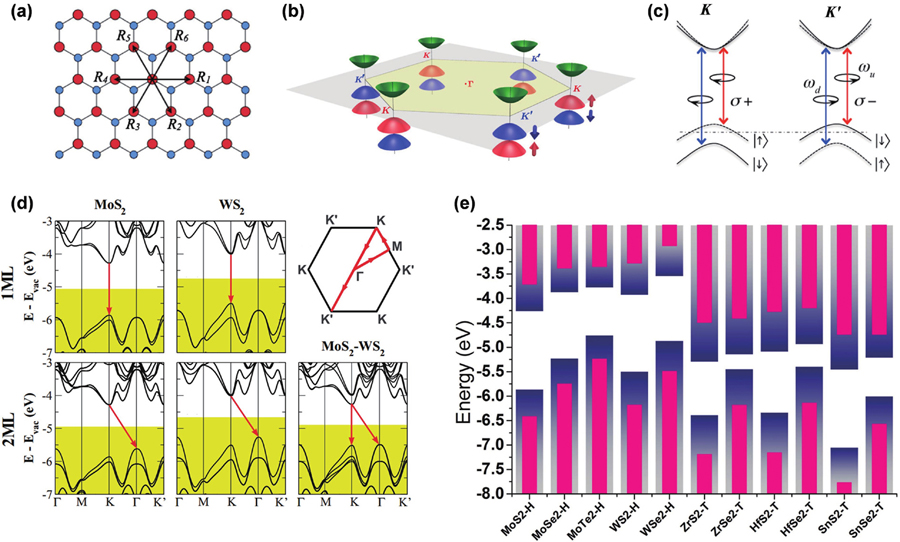
Here, we focus on the semiconducting MX2 compounds with M being Mo or W and X being S, Se or Te. The MX2 compounds have been broadly studied not only because of their stability at ambient conditions, but also benefited by their unique excitonic and valleytronic features. The band structures of TMD monolayers have the extrema at the K and K′ corners of the hexagonal Brillouin zone, which have distinctive spin and valley indices (Figs. 1(a) and1(b))[13-17]. The excitons in TMD monolayers have large binding energies of hundreds of millielectron volts[18] and thus the Bohr radius is only of a few nanometers[19]. Due to the inversion symmetry breaking of TMD monolayers, the excitons are optically addressable based on the valley-contrasting optical selection rules at K and K′ valleys,i.e., direct interband transition in the K (K′) valley couples exclusively with the right (left) circularly polarized light (Figs. 1(b) and1(c))[15,16]. Moreover, the broken inversion symmetry also allows strong spin-orbit coupling of transition metal d orbitals, which are the main components of the conduction and valence bands at K and K′ valleys[20,21]. Strong spin-orbit coupling causes spin splitting at the extrema of the conduction and valence bands, which results in two bright exciton states (electron and hole with the same spin)[22,23]. The two bright excitons are generally referred to as the lower-energy A and higher-energy B excitons. Due to the time-reversal symmetry, the spin splitting has opposite signs in the K and K′ valleys, which couples the spin and valley degrees of freedom[15,16]: the bright exciton is spin up in one valley and spin down in the other (Fig. 1(c)). Therefore, these optical selection rules qualify the emission of excitons in TMD monolayers to carry valley-contrasting optical helicity as well as the spin information of electrons. Additionally, there are also spin- or momentum-forbidden dark excitons with non-zero center-of-mass momentum which are related to photon scattering[24,25]. Those dark excitons can greatly influence the emission properties, especially when their energies are lower than that of the bright excitons.
![(Color online) Features of lattice and band structures of TMD monolayers and heterostructures. (a) 2D hexagonal lattice representing monolayer TMDs.Ri are the vectors connecting nearest metal atoms. (b) Schematic drawing of valley-contrasting splitting at the K and K′ valley of the band structure at the band edges. (c) Spin and valley coupled optical selection rules. K (K′) valley couple toσ+ (σ−) circularly polarized light[15]. Copyright 2012, American Physical Society. (d) Band structures calculated with exchange-correlation energy functions, and the corresponding Brillouin zone (the top right)[31]. Copyright 2013, American Physical Society. (e) Calculated band-edge energies for various TMDs based on ab initio density functional theory calculation using the Perdew-Burke-Ernzerhof functional (blue) and G0W0 (pink), respectively[32]. Copyright 2016, Institute of Physics.](/Images/icon/loading.gif)
Figure 1.(Color online) Features of lattice and band structures of TMD monolayers and heterostructures. (a) 2D hexagonal lattice representing monolayer TMDs.Ri are the vectors connecting nearest metal atoms. (b) Schematic drawing of valley-contrasting splitting at the K and K′ valley of the band structure at the band edges. (c) Spin and valley coupled optical selection rules. K (K′) valley couple toσ+ (σ−) circularly polarized light[15]. Copyright 2012, American Physical Society. (d) Band structures calculated with exchange-correlation energy functions, and the corresponding Brillouin zone (the top right)[31]. Copyright 2013, American Physical Society. (e) Calculated band-edge energies for various TMDs based on ab initio density functional theory calculation using the Perdew-Burke-Ernzerhof functional (blue) and G0W0 (pink), respectively[32]. Copyright 2016, Institute of Physics.
Homobilayers can be either prepared from direct exfoliation from the bulk crystals, or by stacking two monolayers after exfoliation. These two methods lead to disparate optical features corresponding to distinct interband transitions, since the interlayer hybridization between two identical monolayers is significant and highly sensitive to interlayer coupling conditions (Fig. 1(d))[26,27]. In homobilayers, without any band offset, electron and hole states at the K and K′ valleys remain largely localized within each layer, whereas, homobilayers have degenerate exciton states in both layers, which has been manifested as the coexistence of both intralayer and interlayer exciton states at the K and K′ points[28-30].
TMD monolayers (and their alloys[33]) provide diversified band structures. This feature allows people to fabricate heterostructures with different types of band alignments (Fig. 1(e)),i.e. types Ⅰ, Ⅱ, and Ⅲ[34]. The charge transfer behavior is fairly different in three types of heterostructures. For type Ⅰ, the straddling band gap make electrons and holes both accumulate in one component with a smaller bandgap. For type Ⅱ, the staggered band gap with extrema of conduction and valence band in opposite components causes the separation of electrons and holes in different components[35,36]. For type Ⅲ, the band alignment with a broken gap means that the conduction band minimum (CBM) of one component is below the valence band maximum (VBM) of the other. TMD heterobilayers are of type Ⅱ band alignment, with CBM and VBM in different monolayers. The energy offset between the extrema of the conduction or valence band can drive ultrafast interface charge transfer, especially when the interlayer gap is small.
Interlayer gap
In 2D bilayers, besides the band offset of the components, the interlayer coupling at the interface[37] and the electronic structures of bilayers[38] can be readily tuned by increasing[36,37,39] or decreasing[40] the real-space interlayer gap. The states around the K point and T point are insensitive to the interlayer gap, while Г-point states are different (Fig. 2(a))[41]. Here we summarize two types of gap-dependent interlayer interactions,i.e., energy transfer and charge transfer. The charge and energy transfer processes in TMD heterobilayers usually happen in the femto-to-nanosecond timescales and have been investigated in detail using the pump-probe spectroscopy with femtosecond resolution[35,42,43]. The dynamics of charge and energy transfer processes in various low-dimensional materials have been recently reviewed by Huet al.[44].
Figure 2.(Color online) Interlayer gap dependence of energy and charge transfer at the 2D interface. (a) The energies of the band-edge states as a function of the interlayer gap in MoS2/WS2 heterostructures[41]. Copyright 2013, American Physical Society. (b, c) Schemes of Fӧrster and Dexter energy transfer mechanism (left), and schemes (right) of representative TMD heterobilayers showing the direction of Fӧrster and Dexter energy transfer[45,46]. Copyright 2016, American Chemical Society (b) and 2019, American Chemical Society (c). (d) Scheme of WSe2/WS2 heterostructures with different BN intermediate layers. (e) Charge transfer kinetics for heterostructures with different BN layer thicknesses[47]. Copyright 2020, American Chemical Society.
The spin singlet ‘bright’ excitons in TMD monolayers have in-plane dipole moments. When the two layers are efficiently coupled in the heterostructure, the Förster energy transfer takes place, with the exchange energy across the interlayer gap by dipole-dipole interaction (Fig. 2(b))[45,48]. The Förster energy transfer is effective in relatively long distance (<10 nm) and highly dependent on the distance[49]. When the distance is small (<1 nm), another type of energy transfer, namely the Dexter energy transfer emerges. The Dexter energy transfer relies on charge exchange interaction based on the overlap of electron clouds of donor and acceptor. In a type Ⅰ heterobilayer, electrons and holes will both transfer from one monolayer with a larger bandgap to the other with a smaller bandgap, leading to the Dexter energy transfer (Fig. 2(c))[46]. Moreover, the Dexter energy transfer can also occur between spin-forbidden triplet states, based on the Wigner spin conservation rule[46]. Unlike the Förster energy transfer which only allows the energy exchange between bright excitons, the Dexter energy transfer enables the exchange of both bright and dark excitons, thus offering an excellent strategy to brighten the dark exciton in TMD layers.
On another hand, interlayer charge transfer processes profoundly affect the features of each individual component and the heterostructure as a whole. The interlayer gap can efficiently affect the strength of the interlayer coupling and is an important determinant for interlayer charge transfer[50,51]. For closely stacked heterobilayers, ultrafast optical measurements using pump-probe spectroscopy with femtosecond resolution have revealed that the charge transfer takes place within 40 fs in typeⅡ heterobilayers[10,35,42,52,53]. On the other hand, for loosely-contacted heterobilayers, the charge transfer rate was retarded exponentially with increasing distance between the layers. This is in agreement with the distance-dependent electron-transfer rate in the Marcus theory[50,51]. With the increase of layer spacing, the charge transfer related kinetic process gradually slows down (Figs. 2(d) and2(e))[47]. More interestingly, in vertical heterobilayers without any heating or annealing procedure, correlated fluorescence blinking between the two components appears, due to the intermittent interfacial charge transfer across the interlayer gap[36,39,54].
Twist angle
Besides component and interlayer gap, the third basic degree of freedom in interface engineering is twist angle. Following discussions in Section 2.2, it shall be noted that the interlayer distance of stacked 2D heterostructures can slightly vary under different relative orientation (twist) angle between the two monolayers (Figs. 3(a) and3(b))[26,55,56]. According to the dispersion-corrected density functional theory calculations, the equilibrium-state bilayer separation is a function of twist angleθ. The theory indicates that bilayer separation of intermediateθ is larger than that ofθ = 0° and 60° (Fig. 3(a))[26,27]. Furthermore, based on previous theoretical studies, the coupling of Г and Q valleys is huge and insensitive to twist angle in TMDs, which results in strong layer mixing and ultrafast interlayer charge transfer[10,57]. As a comparison, the coupling strengths in K and K′ valleys shall be sensitive to the twist angles[31,41]. When twist angles or lattice mismatches are large, the monolayer electronic states of the K point are largely localized within individual layers, while when the twist angle is small, the interlayer hybridization can occur and cause a direct-to-indirect bandgap change. Therefore, the bandgap of a bilayer exhibits significant dependence on the twist angle[56] (Fig. 3(b)). Moreover, the indirect bandgap is more sensitive to twist angles than the direct ones. According to experimental results from transient absorption spectroscopy, the interlayer charge transfer in TMD heterobilayers was found to be robust, surprisingly independent of the twist angle (Figs. 3(c)–3(f))[42,52]. Such interlayer charge transfer has been theoretically proposed to be associated with the phonon-assisted inter-valley scattering process regardless of crystal orientation[10]. However, the timescale of carrier decay after charge transfer varies with the twist angle. As a result, the recombination of electrons and holes in different layers is profoundly affected by lattice momentum (Figs. 3(c)–3(f))[6,58]. For small twist angles and minor lattice mismatches, TMD heterobilayers exhibit moiré patterns with a large period (compare to the lattice constant), which introduces periodic potential and influence the dynamics of carriers and excitons. In particular, twist-angle engineering in homobilayers and heterobilayers has been applied to realize various emission properties of emerging excitons, such as interlayer excitons and moiré excitons. When the twist angles together with the lattice mismatch are large enough to make the conduction band and valence band misaligned ink space, the emissions of various excitonic species in the heterobilayer are weak. In other words, intralayer exciton emission is quenched because interlayer charge transfer is faster than recombination of intralayer excitons[59]. Meanwhile, the interlayer excitons prefer to go through non-radiative recombination because of the indirect transition path.
Figure 3.(Color online) Twist-angle-dependent features of the 2D interface. (a) Twist-angle dependence of the average layer distance of the WS2/WSe2 heterobilayer based on AA-stacking (blue) and AB-stacking (red) configurations, calculated by dispersion-corrected DFT. (b) Calculated K–K (blue) and Γ–K (red) transition energies for AB-stacked heterobilayers with different twist angles[56]. Copyright 2021, Oxford University Press. (c–e) Transient kinetics in the MoS2 layer for WSe2/MoS2 heterobilayers with three different twist angles, including a single exponential rise (CT: charge transfer process) and a single exponential decay (CR: charge recombination process). (f) Interfacial charge transfer lifetime and charge recombination lifetime as a function of Δϕ (bottom axis) and momentum change (top axis) in WSe2/MoS2 heterojunctions. Inset shows scheme illustrating the twist angle in momentum space[42]. Copyright 2017, American Chemical Society.
Intralayer exciton emission modulated by interfacial engineering
Because of the significant excitonic effects caused by the increased Coulomb interaction, TMD monolayers exhibit a variety of unique exciton states, which dominate their optical properties. In 2D bilayers, the intralayer excitons at the K and K′ valleys within each layer are similar to the individual monolayers but accompanied by additional interactions from the neighboring material[60,61]. The emission of intralayer excitons and the conversion between different exciton states can thereby be profoundly modulated by the change of interface interaction.
2D emitters with boosted emission
Exfoliated monolayer TMDs usually have a limited quantum yield[13]. Pioneering studies have made efforts to boost their emission, with strategies like chemical doping[62], electrical gating and strain tuning[63,64]. In this review, we will mainly focus on representative progress with interface engineering based on interlayer interaction. The broken inversion symmetry of TMD monolayers enables spin splitting at the edges of both valence and conduction bands[15,65,66]. The spin splitting is large at the VBM (hundreds of millielectron volts) but is 10–100 times smaller at the CBM[13,14,22,23,67,68]. As a result of spin splitting, the recombination of electrons and holes with the same spin emits light with different energies, which is attributed to the low-energy A excitons and high-energy B excitons[67]. Besides, there are also nearly degenerate exciton states with higher energy, namely C excitons, that participate in interband transitions according to the absorption spectra of TMD monolayers[67,69]. Usually, the A exciton dominates the emission from TMD monolayers. However, with large exciton oscillator strength, B and C excitons can affect the A exciton emission, especially when the excitation is in resonance with their excitonic energies[70,71].
In a 2D heterobilayer, because of large oscillator strength and parallel dipole orientation in two layers, interlayer energy transfer based on dipole-dipole interaction could realize modulation of emission from a 2D emitter pair. Edaet al.[45] have proved a fast Förster energy transfer process in MoSe2/WS2 heterobilayers. They showed that the Förster coupling between ground state excitons in WS2 layer and higher-order excitons in MoSe2 layer enhances the emission of A excitons in MoSe2 (Figs. 4(a) and4(b)). Besides, the Förster energy transfer can also be mediated by trion with the accumulation of electrons in one component, which leads to an optical gating effect (Figs. 4(c) and4(d))[48]. Such efficient energy transfer offers prospects for optical amplification and energy harvesting through delicate layer engineering. Besides the Förster energy transfer, Zhuet al.[46] discovered ultrafast Dexter energy transfer process in WSe2/MoTe2 van der Waals heterostructures, which enhanced the emission of MoTe2 by transferring the electrons and holes to MoTe2 (Figs. 4(e) and4(f)).
Figure 4.(Color online) Enhanced emission by interfacial interaction in TMD heterostructures. (a, b) Förster energy transfer in MoSe2/WS2 heterobilayers, including photoluminescence excitation intensity map at 78 K where the color scale represents emission intensity (a) and photoluminescence spectra for MoSe2 emission from different heterostructures excited in resonance with A exciton of WS2 (W-A) at 2.00 eV at room temperature (b)[45]. Copyright 2016, American Chemical Society. (c, d) Trion-mediated Förster energy transfer and optical gating effect in WS2/hBN/MoSe2 heterostructures, including the scheme of trion-mediated energy transfer and optical gating effect (c), and photoluminescence spectra at different positions of heterostructures (d)[48]. Copyright 2020, American Chemical Society. (e, f) Dexter energy transfer in WSe2/MoTe2 heterostructures, including photoluminescence spectra of different domains (e) and schematic depiction of near-unity energy transfer of both bright and dark excitons from WSe2 to MoTe2 (f)[46]. Copyright 2019, American Chemical Society. (g, h) Enhanced emission of MoSe2/MoS2 heterostructures by interlayer charge transfer, including a schematic of the band alignment describing the transfer of electrons and holes (g) and photoluminescence intensity maps of the MoSe2/MoS2 with one or two layers h-BNs at the interface. Scale bars are 5μm[72]. Copyright 2016, American Chemical Society.
Interlayer charge transfer is another extensively studied interaction with emerging optical and electrical properties. For semiconductors, the injection of electrons and holes will introduce extra free charges. When these extra charges interact with excitons, they will bind to form charged excitons, called trions[73-75]. Neutral excitons and trions in TMD monolayers are stable at room temperature due to their remarkably large binding energies, hundreds of millielectronvolts[18,19]. Compared with neutral excitons, trions have lower energy and are more likely to go through nonradiative processes such as Auger recombination. In monolayersper se, electrostatic experiments on back-gated devices have indicated that injecting electrons or holes can manipulate excitons and trions in TMD monolayers[76,77]. In TMD heterostructures, the intensity and energy of emissions based on excitonic species in each layer can be changed by interlayer charge transfer at the interface (Figs. 4(g) and4(h)). In MoSe2/MoS2 heterobilayers, interlayer charge transfer significantly enhanced MoSe2 photoluminescence (PL)[72]. Using hexagonal boron nitride (hBN) as the spacer at the interface of MoSe2/MoS2 heterostructures, Kimet al. adjusted the interlayer charge transfer to maximize the MoSe2 PL and achieved a 9-fold increase[72].
Blinking 2D emitters
Fluorescence intermittency, namely fluorescence blinking, has been extensively studied in zero-dimensional systems including quantum dots and molecules[78-80]. The mechanism involves random charge transfer processes or fluctuations in the charge-carrier traps[81]. Xuet al.[36] discovered a new type of blinking effect in the 2D systems for the first time (Figs. 5(a)–5(c)). In the blinking TMD heterobilayers, the weak coupling of layers gives birth to intermittent interfacial charge transfer as well as retained intralayer exciton emission in monolayers. Meanwhile, charge transfer events usually change the doping state of two components with opposite trends. As a result, both the lifetime and the intensity of the two components exhibit negatively correlated fluctuations. Such intermittent interlayer charge transfer events crossing a long-range interfaces have been directly captured by simultaneously record the fluctuating interlayer photocurrent and fluorescence signals (Fig. 5(d))[39]. The spontaneous giant fluctuation of charge carrier density in one layer can even flip the doping type of a semiconductor component, exhibiting either random or controllable switching of positive and negative correlations in a blinking heterobilayer[39]. By designing the interface using WS2 monolayer and Au film, Curtoet al.[54] demonstrated the in-plane correlation of the exciton fluctuation in the WS2 monolayer. Their sample showed spatially correlated PL over tens of micrometers with simultaneous changes in the emission intensity and lifetime. The blinking effect in 2D systems provides a unique platform to study charge carrier dynamics and non-equilibrium physics and shows the potential application in correlated emitters in quantum technology.
Figure 5.(Color online) Fluorescence blinking of 2D emitters. (a) Optical image (left) and fluorescence images (three panels on the right) of a WS2/MoSe2 heterobilayer showing bright, neutral, and dark emission state of WS2 at the heterobilayer region. (b) Spectra of WS2 and MoSe2, and optical image of WS2/MoSe2 heterobilayer (inset). (c) Time-dependent intensity of WS2 (red curve) and MoSe2 (blue curve) emission from the spectra shown in (b)[36]. Copyright 2017, The Authors. (d) Capture of interfacial photocurrent in a blinking WSe2/WS2 circuit at zero bias. The photocurrent and fluorescence intensities are recorded synchronously[39]. Copyright 2021, American Chemical Society.
Intralayer moiré excitons
Owing to the similar hexagonal lattices of TMD monolayers, the superposition of two monolayers with small mismatches forms a superlattice with a relatively larger periodicity as compared to the pristine lattice constant, called the moiré superlattice. The large periodic lattices can dramatically modify the electronic states and create a new periodic potential for carriers and excitons, namely moiré potential[82]. According to theoretical studies, the moiré potential has extrema that are generally centered at the high-symmetry positions of the superlattice (Fig. 6(a)). The moiré potential can influence the dispersion of intralayer excitons and localize excitons at different high-symmetry positions in the superlattice (Fig. 6(b))[82,83]. Intralayer exciton states are separated into multiple states by moiré periodical potential[84-89], which leads to finite-momentum exciton states and modifies optical selection rules. In WS2/WS2 homobilayers with a twist angle of 1.46°, the emission spectra show multiple peaks with constant energy difference (Figs. 6(c) and6(d))[87], which is attributed to the confined intralayer excitons by moiré potential. Moreover, localized moiré intralayer excitons are sensitive to the moiré periodicity. In a twisted WSe2/WSe2 homobilayer, the moiré superlattice has two high-symmetry positions with high and low potential energy, respectively. When the moiré periodicity is small, the high-energy excitons will relax and move to the low-energy position and then emit. Emission from the high-energy excitons can emerge in the region with large moiré periodicity (>10 nm) when the length of the moiré period is beyond the reach of exciton diffusion before the recombination. (Figs. 6(e) and6(f))[88]. Localized moiré intralayer excitons have been observed in several moiré systems and become a powerful and interesting platform for investigating correlated excitonic states.
Figure 6.(Color online) Intralayer moiré excitons in TMD heterostructures. (a) Left: schematic illustration of the moiré superlattice with a twist angleθ and moiré potential periodaM. Right: the moiré Brillouin zone corresponding to the moiré unit cell. (b) Schematic diagram of excitons trapped by the periodic moiré potential. (c) Observation of moiré excitons in twisted WS2/WS2 homobilayer superlattices. (d) Linear energy distribution of different peaks fitted by the Lorentzian function[87]. Copyright 2022, American Physical Society. (e, f) Excitons in a reconstructed moiré potential. (e) Scanning electron microscopy image of twisted WSe2 bilayer showing a reconstructed moiré pattern[90]. Copyright 2021, Wiley-VCH GmbH. (f) Photoluminescence spectra at five positions in a WSe2 homobilayer[91]. Copyright 2022, Royal Society of Chemistry.
Interlayer exciton emission modulated by interfacial engineering
Most combinations of common TMD monolayers (e.g., WS2, MoS2, WSe2, and MoSe2) feature ultrafast interlayer charge transfer, causing electrons and holes to separate and reside in different layers, respectively. The Coulomb interactions between adjacent layers allow the generation of electron-hole pairs with out-of-plane electrical dipole moments, to form the interlayer excitons. Lots of interest has been attracted into the unique properties of interlayer excitons like their long lifetime[59,92], quantum-confined Stark effect[93], valley polarization and high-temperature (~100 K) exciton condensation[94]. Unlike intralayer excitons that can be studied via absorption spectroscopy, interlayer excitons have weak oscillator strengths and are generally probed by emission spectra. Luminescence from the interlayer exciton also belongs to the field of 2D emitters and can be highly modified through interface engineering, which is worth looking into.
Interlayer excitons
The efficient formation of interlayer excitons requires certain prerequisites: suitable interlayer gap and proper twist angle between TMD monolayers in heterostructures. In type Ⅱ heterostructures, owing to the small interlayer gap that contributes to the interlayer charge transfer, the Coulomb interaction between two layers is strong enough to produce interlayer excitons, with smaller binding energy and lower emission energy compared to the intralayer excitons of both components (Fig. 7(a))[59]. In addition, the alignment of the conduction and valence bands ink space contributes to the radiative recombination of electrons and holes located in different layers. The relative twist angles between the two layers also shift the electron and hole bands in momentum space (k space). Thus, the PL energies and intensities of interlayer excitons exhibit distinct dependence on the twist angle[27,55,99]. By combining photoluminescence spectroscopy and first-principles calculations, Kunstmannet al.[100] identified that the electrons and holes of interlayer excitons in MoS2/WSe2 heterostructures locate at the K point and Γ point respectively (Figs. 7(b) and7(c)). Compared with the K–K transition, the Γ–K transition is in quantitative agreement with the experiment. The valence band maximum at the Γ valley is a hybrid state of both layers and it moves upwards as hybridization increases. Shinet al.[97] reported that the emission of interlayer excitons in MoSe2/WSe2 heterostructures increases with twist angle around 0° and 60° and disappeared at 10°–50° (Fig. 7(d)). Highly aligned Brillouin zones of two monolayers promotes the efficient formation and radiative recombination of interlayer excitons[6,97,101,102]. Moreover, the emission energy of interlayer excitons is associated with the twist-angle dependence of interlayer coupling strength (Fig. 7(e)). In homobilayers with a small twist angle, interlayer excitons can coexist with intralayer excitons in the same K or K′ valley[28-30], forming a hybrid exciton state.
Figure 7.(Color online) Emission features of interlayer excitons in TMD heterostructures. (a) Photoluminescence of WSe2 and MoSe2 monolayers and the heterobilayers[95]. Copyright 2022, Royal Society of Chemistry. (b) Interlayer exciton energies and calculated transition energies for heterobilayers with different twist angles. (c) Left: band alignment diagram. Right: the misaligned Brillouin zones of MoS2 (blue) and WSe2 (green) where both K–K and Γ–K transitions arek-space indirect[96]. Copyright 2020, Royal Society of Chemistry. (d) Intensity and (e) energy of the interlayer exciton emission versus the twist angle. The inset in (d) shows the schema of MoSe2/WSe2 heterobilayers[97]. Copyright 2017, American Chemical Society. (f, g) Spin-valley polarization of the interlayer exciton in MoSe2/WSe2 heterostructures. (f) Circular polarization-resolved photoluminescence spectra of the interlayer exciton showing the generation of strong valley polarization. (g) Spatial maps ofσ+ (left) andσ− (right) interlayer exciton photoluminescence[98]. Copyright 2016, Science.
The spin-valley information of electrons in TMD monolayers is a unique quantum index of intralayer excitons. For interlayer excitons, due to the breaking of the out-of-plane mirror symmetry, the restriction of spin conservation is no longer valid. As a result, the optical transition dipole of the spin-triplet exciton is in the same order of magnitude as that of the spin-singlet exciton[103]. Riveraet al.[98] realized valley-specific interlayer excitons in WSe2/MoSe2 vertical heterostructures using circularly polarized optical pumping (Fig. 7(f)). The valley lifetime of circular polarization-resolved emission from the interlayer exciton was measured to be ~40 ns, which allows visualization of lateral diffusion (Fig. 7(g)). Moreover, interlayer excitons are not confined to the bilayers. In multilayer heterostructures constructed by stacking TMD monolayer and few layers, emission from interlayer excitons can be obtained and engineered[104]. The spin- and valley-contrasting emission of interlayer excitons has been demonstrated in various 2D bilayer systems. This allows optical addressing of both the spin and valley configuration of interlayer excitons, and makes TMD heterostructures promising in device technologies based on valleytronics.
Interlayer moiré excitons
As discussed in Section 2.3, the moiré superlattice formed by two TMD monolayers produces a periodic potential that can localize intralayer excitons. Similarly, there is also a potential landscape for interlayer excitons in the moiré superlattice (Figs. 8(a)–8(c)), which generates localized states and provides exotic emission features[105,106]. The low-energy interlayer exciton states are typically localized at the high-symmetry positions of the moiré superlattice. The specific high-symmetry position offers the electron and hole with different rotation centers, leading to an additional angular momentum. Thus, the emission of interlayer excitons is modulated by moiré reciprocal lattice vectors[107-109], leading to finite momentum of optically active exciton states. According to the theoretical analyses, the interlayer excitons at different high-symmetry points follow different optical selection rules[107,109]. The helicity-resolved photoluminescence from heterobilayers with different twist angles reveals valley polarization of trapped interlayer excitons (Figs. 8(d) and8(e)). Additionally, in the moiré superlattice formed by bilayer MoSe2 and monolayer WSe2, Brotons-Gisbertet al.[110] observed maintenance of strong valley polarization of interlayer exciton from corresponding components, which is attributed to spin-layer locking of interlayer excitons trapped in moiré potentials.
Figure 8.(Color online) Modulated emissions of interlayer moiré excitons in TMD heterostructures. (a) A moiré superlattice formed by a MoSe2/WSe2 vertical heterostructure, showing three highlighted regions with three-fold rotational symmetry. (b) Optical selection rules of different atomic configurations in K valley. (c) Left: the moiré potential of the interlayer exciton transition, showing a local minimum and maximum at different sites. Right: spatial map of the degree of circular polarization for K-valley excitons[111]. Copyright 2021, Springer Nature. (d, e) Helicity-resolved photoluminescence spectra of trapped interlayer excitons in MoSe2/WSe2 heterobilayers with twist angles of (d) 57° and (e) 2°[112]. Copyright 2021, Royal Society of Chemistry. (f-h), Modulation of interlayer moiré excitons by strain, which changes the moiré patterns. (f, g) Piezoresponse force microscopy (PFM) images at two locations of the heterostructure subjected to stress[113]. Copyright 2021, Wiley‐VCH GmbH. (h) Excitation power-dependent emission spectra of 1D moiré exciton[114]. Copyright 2021, American Chemical Society. (i) Trapped interlayer trions in a moiré superlattice[115]. Copyright 2021, Nature.
In addition to the twist angle that determines the superlattice geometry, in-plane and out-of-plane strain is another decisive factor to influence the periodicity of moiré potentials. The spatially inhomogeneous superlattice structure with different periodicity induced by strain exhibits different emission characteristics in different regions[88]. Baiet al.[116] have presented strain-induced one-dimensional moiré patterns, in which the emission from excitons shows linear polarization and higher intensity than that in zero-dimensional moiré potentials (Figs. 8(f)–8(h)). Such sensitivity to strain field provides a new path to control the moiré potential landscape as well as the excitonic dynamics in TMD heterobilayers, leading to the potential application of responsive optical and electronic devices. When the moiré excitons are coupled to charge carriers, the charge-coupled moiré excitons (moiré trions) can emerge (Fig. 8(i))[105,115,117]. The studies show that moiré trions exhibit sharp emission lines with high sensitivity to sample inhomogeneity (Fig. 8(i)). Baeket al.[115] have realized spectrally tracking of the emitters as the moiré excitons are charged by excess carriers. They also discovered stepwise changes in the moiré trions emission energy resulted from the Coulomb interactions from carriers at the nearest-neighbor moiré sites. The emission features of moiré trions can sensor to characterize Coulomb interaction and visualize charge correlated states, which can be used to judge the uniformity of moiré superlattices.
Moiré quantum emitters
Quantum emitters, known as “single-photon emitters”, are crucial for photon-based quantum information processing in quantum technologies. In TMD monolayers, the localized excitons trapped by defects can show the single-photon nature with narrow line widths of around 100μeV and strong photon antibunching[120-125]. In TMD moiré superlattices, the excitons confined by the periodical moiré potential, namely moiré excitons, are predicted to become quantum emitters. This is reasonable due to the large oscillator strength of the interlayer exciton and the strong variation (~116 meV) of moiré potential around the minima (A point) (Fig. 9(a))[109]. In heterobilayers moiré superlattices, the previously broad emission from interlayer excitons under relatively high-powered excitation can turn into multiple narrow peaks with linewidth down to around 100μeV, when the power of excitation is low (Fig. 9(b))[110,119,126,127]. Based on the periodical moiré potentials, Yuet al.[109] have simulated highly uniform and ordered nanodot arrays of quantum emitters. They found that the moiré-trapped interlayer excitons with long lifetimes can be tuned from quantum emitters to excitonic superlattices with giant spin-orbit coupling by applying the electric field or strain. Baeket al.[119] found the photon antibunching phenomenon from a single moiré-trapped interlayer exciton in a MoSe2/WSe2 heterobilayer (Figs. 9(c)–9(f)). They demonstrated that the discrete anharmonic spectra arise from electron-hole pairs trapped in moiré potentials, which exhibits opportunities to investigate the single-photon emitters with high tunability.
Figure 9.(Color online) Quantum emission from moiré excitons. (a) Nano-patterned quantum emitter arrays. Left: distribution of oscillator strength of the interlayer exciton. Right: nanodot confinements atA points, realizing a periodic array of excitonic quantum emitters. Three high-symmetry points corresponding to the moiré superlattices are labeled asA,B, andC, respectively[109]. Copyright 2017, Science. (b) Normalized emission spectra excited by photon energy of 1.55 eV with different excitation power densities[118]. Copyright 2021, American Chemical Society. (c–f) Quantum features of moiré interlayer excitons. (c) Photoluminescence spectrum of MoSe2/WSe2 moiré superlattices at 4 K. (d) Time-resolved normalized PL intensity of the single emitter fitted by single exponential decay fit (red line), which reveals a lifetime of 12.1 ± 0.3 ns. (e) Integrated PL intensity of the same single emission peak (1.401 eV) at different excitation powers. (f) Photon antibunching revealed by second-order photon correlation statistics (g(2)(τ)) of emission with the experimental data (red solid line) and the Poissonian interval error (red shadowed area)[119]. Copyright 2020, Science.
Summary and outlook
In summary, we have reviewed progress on novel van der Waals emitters based on well-designed homo- or heterojunctions, representative observations are summarized inTable 1. The excellent excitonic features of TMD heterostructures enable exploration of many-body quantum phenomena[128,129] and development of novel devices, such as valleytronic devices[16], excitonic transistors[130,131], switches[132], lasers[133,134], and photodetectors[135]. Nevertheless, challenges need to be taken up to push the boundary of the field of excitonic physics and to realize applications in even broader scenarios. Firstly, to better make use of the wide tunability of excitons in TMD heterostructures, more efforts are needed to tailor the absorption and emission of excitons. Methods such as coupling heterostructures with cavities[134] and plasmonic materials[136,137] show additional promise in the design of light sources and other photonic applications. Secondly, the substantial binding energies and long optical lifetimes of interlayer excitons provide opportunities for the realization of high-temperature Bose-Einstein condensation with excitons, which is still an area that needs to be meticulously explored. Thirdly, interlayer excitons possess a sufficiently high degree of valley polarization and long valley-polarized lifetime at room temperature, thanks to their significantly suppressed intervalley scattering. These features are crucial for the practical processing of valley information carried by polarized light. Finally, in moiré superlattices, the trapped excitons at the moiré potential minima enable single photon emission, but impede the exciton transport[138]. It remains a challenge to modulate and characterize moiré quantum emitters localized at the moiré potential. Moreover, the periodical moiré unit cells support the formation of identical quantum emitters, which holds the promise for large-scale integration of coherent quantum-emitter array needless of extra modulation.
| Interface engineering method | Interface parameter | Component | Properties |
|---|
| a The phenomenon shall be robust for almost all angles. |
| b In these works, thermal annealing is applied to reach a closely packed state with an estimated interlayer distance of 0.6–0.7 nm. |
| Interlayer gapa | ~ 10 Å | WSe2/MoTe2[46] | Dexter energy transfer |
| < 10 nm | MoSe2/WS2[45] | Förster energy transfer |
| 2-5 nm, no spacing layer | WS2/MoSe2[36] | Fluorescence blinking |
| WS2/WSe2[39] |
| Twist angleb | 2° | MoSe2/WS2[139] | Hybridized exciton |
| 0.5 ± 0.3° | WSe2/WS2[85] | Intralayer moiré exciton |
| 1.5° | WSe2/WS2[87] |
| < 5° | WSe2/WSe2[88] |
| 1.36° | WSe2/WSe2[89] |
| 0°/60° | MoSe2/WSe2[59] | Long-live interlayer exciton |
| 0°–60° | MoSe2/WSe2[102] | k-space indirect interlayer exciton |
| MoS2/WSe2[100] |
| WS2/WSe2[56] |
| ~0°/~60° | MoSe2/WSe2[98] | Valley polarized interlayer exciton |
| 2°/20°/57° | MoSe2/WSe2[126] |
| 58.7°± 0.7° | WSe2/MoSe2[140] |
| 2°/20°/57° | MoSe2/WSe2[126] | Interlayer moiré exciton |
| ~1° | MoSe2/WSe2[106] |
| 56.7 ± 0.2° | MoSe2/WSe2[115] | Interlayer moiré trion |
| ~60° | MoSe2/WSe2[117] |
| 57.5° | MoSe2/WSe2[105] |
| 0°/60° | MoSe2/WSe2 (MoS2/WSe2)[109] | Moiré quantum emitter |
| < 1° | MoSe2/WSe2 (MoS2/WS2)[141] |
| ~60° | MoSe2/WSe2[119] |
Table 1. Primary progresses on novel van der Waals emitters based on interface engineering.
References
[1] R Rossetti, S Nakahara, L E Brus. Quantum size effects in the redox potentials, resonance Raman spectra, and electronic spectra of CdS crystallites in aqueous solution. J Chem Phys, 79, 1086(1983).
[2] L E Brus. Electron-electron and electron-hole interactions in small semiconductor crystallites: The size dependence of the lowest excited electronic state. J Chem Phys, 80, 4403(1984).
[3] C Chang, W Chen, Y Chen et al. Recent progress on two-dimensional materials. Acta Phys Chim Sinica, 37, 2108017(2021).
[4] F C Wu, F Y Qu, A H MacDonald. Exciton band structure of monolayer MoS2. Phys Rev B, 91, 075310(2015).
[5] A Ramasubramaniam. Large excitonic effects in monolayers of molybdenum and tungsten dichalcogenides. Phys Rev B, 86, 115409(2012).
[6] H Heo, J H Sung, S Cha et al. Interlayer orientation-dependent light absorption and emission in monolayer semiconductor stacks. Nat Commun, 6, 7372(2015).
[7] L Wang, I Meric, P Y Huang et al. One-dimensional electrical contact to a two-dimensional material. Science, 342, 614(2013).
[8] K Kim, M Yankowitz, B Fallahazad et al. Van der waals heterostructures with high accuracy rotational alignment. Nano Lett, 16, 1989(2016).
[9] R Frisenda, E Navarro-Moratalla, P Gant et al. Recent progress in the assembly of nanodevices and van der Waals heterostructures by deterministic placement of 2D materials. Chem Soc Rev, 47, 53(2018).
[10] Y Wang, Z Wang, W Yao et al. Interlayer coupling in commensurate and incommensurate bilayer structures of transition-metal dichalcogenides. Phys Rev B, 95, 115429(2017).
[11] E C Regan, D Q Wang, E Y Paik et al. Emerging exciton physics in transition metal dichalcogenide heterobilayers. Nat Rev Mater, 7, 778(2022).
[12] A K Geim, I V Grigorieva. Van der waals heterostructures. Nature, 499, 419(2013).
[13] K F Mak, C G Lee, J Hone et al. Atomically thin MoS2: A new direct-gap semiconductor. Phys Rev Lett, 105, 136805(2010).
[14] A Splendiani, L Sun, Y B Zhang et al. Emerging photoluminescence in monolayer MoS2. Nano Lett, 10, 1271(2010).
[15] D Xiao, G B Liu, W X Feng et al. Coupled spin and valley physics in monolayers of MoS2 and other group-VI dichalcogenides. Phys Rev Lett, 108, 196802(2012).
[16] X D Xu, W Yao, D Xiao et al. Spin and pseudospins in layered transition metal dichalcogenides. Nat Phys, 10, 343(2014).
[17] W J Li, X Lu, J T Wu et al. Optical control of the valley Zeeman effect through many-exciton interactions. Nat Nanotechnol, 16, 148(2021).
[18] A Chernikov, T C Berkelbach, H M Hill et al. Exciton binding energy and nonhydrogenic rydberg series in monolayer WS2. Phys Rev Lett, 113, 076802(2014).
[19] T C Berkelbach, M S Hybertsen, D R Reichman et al. Theory of neutral and charged excitons in monolayer transition metal dichalcogenides. Phys Rev B, 88, 045318(2013).
[20] W Yao, D Xiao, Q Niu. Valley-dependent optoelectronics from inversion symmetry breaking. Phys Rev B, 77, 235406(2008).
[21] D Xiao, W Yao, Q Niu. Valley-contrasting physics in graphene: Magnetic moment and topological transport. Phys Rev Lett, 99, 236809(2007).
[22] K Kośmider, J W González, J Fernández-Rossier. Large spin splitting in the conduction band of transition metal dichalcogenide monolayers. Phys Rev B, 88, 245436(2013).
[23] J P Echeverry, B Urbaszek, T Amand et al. Splitting between bright and dark excitons in transition metal dichalcogenide monolayers. Phys Rev B, 93, 121107(2016).
[24] G Berghäuser, P Steinleitner, P Merkl et al. Mapping of the dark exciton landscape in transition metal dichalcogenides. Phys Rev B, 98, 020301(2018).
[25] P Merkl, F Mooshammer, P Steinleitner et al. Ultrafast transition between exciton phases in van der Waals heterostructures. Nat Mater, 18, 691(2019).
[26] K H Liu, L M Zhang, T Cao et al. Evolution of interlayer coupling in twisted molybdenum disulfide bilayers. Nat Commun, 5, 4966(2014).
[27] A M van der Zande, J Kunstmann, A Chernikov et al. Tailoring the electronic structure in bilayer molybdenum disulfide via interlayer twist. Nano Lett, 14, 3869(2014).
[28] L Meckbach, T Stroucken, S W Koch. Influence of the effective layer thickness on the ground-state and excitonic properties of transition-metal dichalcogenide systems. Phys Rev B, 97, 035425(2018).
[29] J Horng, T Stroucken, L Zhang et al. Observation of interlayer excitons in MoSe2 single crystals. Phys Rev B, 97, 241404(2018).
[30] A Arora, M Drüppel, R Schmidt et al. Interlayer excitons in a bulk van der Waals semiconductor. Nat Commun, 8, 639(2017).
[31] K Kośmider, J Fernández-Rossier. Electronic properties of the MoS2-WS2 heterojunction. Phys Rev B, 87, 075451(2013).
[32] C X Zhang, C Gong, Y F Nie et al. Systematic study of electronic structure and band alignment of monolayer transition metal dichalcogenides in Van der Waals heterostructures. 2D Mater, 4, 015026(2016).
[33] Y F Chen, J Y Xi, D O Dumcenco et al. Tunable band gap photoluminescence from atomically thin transition-metal dichalcogenide alloys. ACS Nano, 7, 4610(2013).
[34] C Gong, H J Zhang, W H Wang et al. Band alignment of two-dimensional transition metal dichalcogenides: Application in tunnel field effect transistors. Appl Phys Lett, 103, 053513(2013).
[35] X P Hong, J Kim, S F Shi et al. Ultrafast charge transfer in atomically thin MoS2/WS2 heterostructures. Nat Nanotechnol, 9, 682(2014).
[36] W G Xu, W W Liu, J F Schmidt et al. Correlated fluorescence blinking in two-dimensional semiconductor heterostructures. Nature, 541, 62(2017).
[37] H Fang, C Battaglia, C Carraro et al. Strong interlayer coupling in van der Waals heterostructures built from single-layer chalcogenides. Proc Natl Acad Sci USA, 111, 6198(2014).
[38] E S Kadantsev et al. Electronic structure of a single MoS2 monolayer. Solid State Commun, 152, 909(2012).
[39] H Li, H L Li, X Z Wang et al. Spontaneous polarity flipping in a 2D heterobilayer induced by fluctuating interfacial carrier flows. Nano Lett, 21, 6773(2021).
[40] J Xia, J X Yan, Z H Wang et al. Strong coupling and pressure engineering in WSe2–MoSe2 heterobilayers. Nat Phys, 17, 92(2021).
[41] H P Komsa, A V Krasheninnikov. Electronic structures and optical properties of realistic transition metal dichalcogenide heterostructures from first principles. Phys Rev B, 88, 085318(2013).
[42] H M Zhu, J Wang, Z Z Gong et al. Interfacial charge transfer circumventing momentum mismatch at two-dimensional van der waals heterojunctions. Nano Lett, 17, 3591(2017).
[43] Y Zeng, W Dai, R D Ma et al. Distinguishing ultrafast energy transfer in atomically thin MoS2/WS2 heterostructures. Small, 18, e2204317(2022).
[44] Z Hu, X Liu, P L Hernández-Martínez et al. Interfacial charge and energy transfer in van der Waals heterojunctions. InfoMat, 4, e12290(2022).
[45] D Kozawa, A Carvalho, I Verzhbitskiy et al. Evidence for fast interlayer energy transfer in MoSe2/WS2 heterostructures. Nano Lett, 16, 4087(2016).
[46] L L Wu, Y Z Chen, H Z Zhou et al. Ultrafast energy transfer of both bright and dark excitons in 2D van der waals heterostructures beyond dipolar coupling. ACS Nano, 13, 2341(2019).
[47] H Z Zhou, Y D Zhao, W J Tao et al. Controlling exciton and valley dynamics in two-dimensional heterostructures with atomically precise interlayer proximity. ACS Nano, 14, 4618(2020).
[48] Z H Hu, P L Hernández-Martínez, X Liu et al. Trion-mediated Förster resonance energy transfer and optical gating effect in WS2/hBN/MoSe2 heterojunction. ACS Nano, 14, 13470(2020).
[49] S K Lyo. Energy transfer from an electron-hole plasma layer to a quantum well in semiconductor structures. Phys Rev B, 81, 115303(2010).
[50] R A Marcus. Chemical and electrochemical electron-transfer theory. Annu Rev Phys Chem, 15, 155(1964).
[51] R A Marcus et al. Electron transfers in chemistry and biology. Biochim Biophys Acta Rev Bioenerg, 811, 265(1985).
[52] Z H Ji, H Hong, J Zhang et al. Robust stacking-independent ultrafast charge transfer in MoS2/WS2 bilayers. ACS Nano, 11, 12020(2017).
[53] X Y Zhu, N R Monahan, Z Z Gong et al. Charge transfer excitons at van der waals interfaces. J Am Chem Soc, 137, 8313(2015).
[54] R H Godiksen, S J Wang, T V Raziman et al. Correlated exciton fluctuations in a two-dimensional semiconductor on a metal. Nano Lett, 20, 4829(2020).
[55] P Merkl, F Mooshammer, S Brem et al. Twist-tailoring Coulomb correlations in van der Waals homobilayers. Nat Commun, 11, 2167(2020).
[56] K Wu, H X Zhong, Q B Guo et al. Identification of twist-angle-dependent excitons in WS2/WSe2 heterobilayers. Natl Sci Rev, 9, nwab135(2021).
[57] Q J Zheng, W A Saidi, Y Xie et al. Phonon-assisted ultrafast charge transfer at van der waals heterostructure interface. Nano Lett, 17, 6435(2017).
[58] K Wang, B Huang, M K Tian et al. Interlayer coupling in twisted WSe2/WS2 bilayer heterostructures revealed by optical spectroscopy. ACS Nano, 10, 6612(2016).
[59] P Rivera, J R Schaibley, A M Jones et al. Observation of long-lived interlayer excitons in monolayer MoSe2–WSe2 heterostructures. Nat Commun, 6, 6242(2015).
[60] A Raja, A Chaves, J Yu et al. Coulomb engineering of the bandgap and excitons in two-dimensional materials. Nat Commun, 8, 15251(2017).
[61] L Waldecker, A Raja, M Rösner et al. Rigid band shifts in two-dimensional semiconductors through external dielectric screening. Phys Rev Lett, 123, 206403(2019).
[62] M Amani, D H Lien, D Kiriya et al. Near-unity photoluminescence quantum yield in MoS2. Science, 350, 1065(2015).
[63] D H Lien, S Z Uddin, M Yeh et al. Electrical suppression of all nonradiative recombination pathways in monolayer semiconductors. Science, 364, 468(2019).
[64] H Kim, S Z Uddin, N Higashitarumizu et al. Inhibited nonradiative decay at all exciton densities in monolayer semiconductors. Science, 373, 448(2021).
[65] Z Y Zhu, Y C Cheng, U Schwingenschlögl. Giant spin-orbit-induced spin splitting in two-dimensional transition-metal dichalcogenide semiconductors. Phys Rev B, 84, 153402(2011).
[66] G B Liu, D Xiao, Y G Yao et al. Electronic structures and theoretical modelling of two-dimensional group-VIB transition metal dichalcogenides. Chem Soc Rev, 44, 2643(2015).
[67] W J Zhao, Z Ghorannevis, L Q Chu et al. Evolution of electronic structure in atomically thin sheets of WS2 and WSe2. ACS Nano, 7, 791(2013).
[68] H L Zeng, G B Liu, J F Dai et al. Optical signature of symmetry variations and spin-valley coupling in atomically thin tungsten dichalcogenides. Sci Rep, 3, 1608(2013).
[69] J A Wilson, A D Yoffe. The transition metal dichalcogenides discussion and interpretation of the observed optical, electrical and structural properties. Adv Phys, 18, 193(1969).
[70] A Arora, M Koperski, K Nogajewski et al. Excitonic resonances in thin films of WSe2: From monolayer to bulk material. Nanoscale, 7, 10421(2015).
[71] D Kozawa, R Kumar, A Carvalho et al. Photocarrier relaxation pathway in two-dimensional semiconducting transition metal dichalcogenides. Nat Commun, 5, 4543(2014).
[72] M S Kim, C Seo, H Kim et al. Simultaneous hosting of positive and negative trions and the enhanced direct band emission in MoSe2/MoS2 heterostacked multilayers. ACS Nano, 10, 6211(2016).
[73] M A Lampert. Mobile and immobile effective-mass-particle complexes in nonmetallic solids. Phys Rev Lett, 1, 450(1958).
[74] K Kheng, R T Cox, D A My et al. Observation of negatively charged excitons X- in semiconductor quantum wells. Phys Rev Lett, 71, 1752(1993).
[75] G Finkelstein, H Shtrikman. Optical spectroscopy of a two-dimensional electron gas near the metal-insulator transition. Phys Rev Lett, 74, 976(1995).
[76] J S Ross, S F Wu, H Y Yu et al. Electrical control of neutral and charged excitons in a monolayer semiconductor. Nat Commun, 4, 1474(2013).
[77] K F Mak, K L He, C G Lee et al. Tightly bound trions in monolayer MoS2. Nat Mater, 12, 207(2013).
[78] W Nagourney, J Sandberg, H Dehmelt. Shelved optical electron amplifier: Observation of quantum jumps. Phys Rev Lett, 56, 2797(1986).
[79] T Basché, S Kummer, C Bräuchle. Direct spectroscopic observation of quantum jumps of a single molecule. Nature, 373, 132(1995).
[80] R M Dickson, A B Cubitt, R Y Tsien et al. On/off blinking and switching behaviour of single molecules of green fluorescent protein. Nature, 388, 355(1997).
[81] C Galland, Y Ghosh, A Steinbrück et al. Two types of luminescence blinking revealed by spectroelectrochemistry of single quantum dots. Nature, 479, 203(2011).
[82] F C Wu, T Lovorn, A H MacDonald. Topological exciton bands in moiré heterojunctions. Phys Rev Lett, 118, 147401(2017).
[83] N Zhang, A Surrente, M Baranowski et al. Moiré intralayer excitons in a MoSe2/MoS2 heterostructure. Nano Lett, 18, 7651(2018).
[84] Y H Tang, J Gu, S Liu et al. Tuning layer-hybridized moiré excitons by the quantum-confined Stark effect. Nat Nanotechnol, 16, 52(2021).
[85] C H Jin, E C Regan, A M Yan et al. Observation of moiré excitons in WSe2/WS2 heterostructure superlattices. Nature, 567, 76(2019).
[86] Y H Tang, L Z Li, T X Li et al. Simulation of Hubbard model physics in WSe2/WS2 moiré superlattices. Nature, 579, 353(2020).
[87] B Wu, H H Zheng, S F Li et al. Observation of moiré excitons in the twisted WS2/WS2 homostructure. Nanoscale, 14, 12447(2022).
[88] T I Andersen, G Scuri, A Sushko et al. Excitons in a reconstructed moiré potential in twisted WSe2/WSe2 homobilayers. Nat Mater, 20, 480(2021).
[89] B Wu, H H Zheng, S F Li et al. Evidence for moiré intralayer excitons in twisted WSe2/WSe2 homobilayer superlattices. Light Sci Appl, 11, 166(2022).
[90] Y D Liu, A Elbanna, W B Gao et al. Interlayer excitons in transition metal dichalcogenide semiconductors for 2D optoelectronics. Adv Mater, 34, e2107138(2022).
[91] Y P Liu, C Zeng, J Yu et al. Moiré superlattices and related moiré excitons in twisted van der Waals heterostructures. Chem Soc Rev, 50, 6401(2021).
[92] C Y Jiang, W G Xu, A Rasmita et al. Microsecond dark-exciton valley polarization memory in two-dimensional heterostructures. Nat Commun, 9, 753(2018).
[93] S Dufferwiel, S Schwarz, F Withers et al. Exciton–polaritons in van der Waals heterostructures embedded in tunable microcavities. Nat Commun, 6, 8579(2015).
[94] Z F Wang, D A Rhodes, K Watanabe et al. Evidence of high-temperature exciton condensation in two-dimensional atomic double layers. Nature, 574, 76(2019).
[95] J Ji, J H Choi. Recent progress in 2D hybrid heterostructures from transition metal dichalcogenides and organic layers: Properties and applications in energy and optoelectronics fields. Nanoscale, 14, 10648(2022).
[96] D B Sulas-Kern, E M Miller, J L Blackburn. Photoinduced charge transfer in transition metal dichalcogenide heterojunctions - towards next generation energy technologies. Energy Environ Sci, 13, 2684(2020).
[97] P K Nayak, Y Horbatenko, S Ahn et al. Probing evolution of twist-angle-dependent interlayer excitons in MoSe2/WSe2 van der waals heterostructures. ACS Nano, 11, 4041(2017).
[98] P Rivera, K L Seyler, H Y Yu et al. Valley-polarized exciton dynamics in a 2D semiconductor heterostructure. Science, 351, 688(2016).
[99] E Marcellina, X Liu, Z H Hu et al. Evidence for moiré trions in twisted MoSe2 homobilayers. Nano Lett, 21, 4461(2021).
[100] J Kunstmann, F Mooshammer, P Nagler et al. Momentum-space indirect interlayer excitons in transition-metal dichalcogenide van der Waals heterostructures. Nat Phys, 14, 801(2018).
[101] W Yan, L Meng, Z S Meng et al. Probing angle-dependent interlayer coupling in twisted bilayer WS2. J Phys Chem C, 123, 30684(2019).
[102] A T Hanbicki, H J Chuang, M R Rosenberger et al. Double indirect interlayer exciton in a MoSe2/WSe2 van der waals heterostructure. ACS Nano, 12, 4719(2018).
[103] H Y Yu, G B Liu, W Yao. Brightened spin-triplet interlayer excitons and optical selection rules in van der Waals heterobilayers. 2D Mater, 5, 035021(2018).
[104] Q H Tan, A Rasmita, S Li et al. Layer-engineered interlayer excitons. Sci Adv, 7, eabh0863(2021).
[105] E F Liu, E Barré, J van Baren et al. Signatures of moiré trions in WSe2/MoSe2 heterobilayers. Nature, 594, 46(2021).
[106] K Tran, G Moody, F C Wu et al. Evidence for moiré excitons in van der waals heterostructures. Nature, 567, 71(2019).
[107] H Y Yu, Y Wang, Q J Tong et al. Anomalous light cones and valley optical selection rules of interlayer excitons in twisted heterobilayers. Phys Rev Lett, 115, 187002(2015).
[108] F C Wu, T Lovorn, A H MacDonald. Theory of optical absorption by interlayer excitons in transition metal dichalcogenide heterobilayers. Phys Rev B, 97, 035306(2018).
[109] H Y Yu, G B Liu, J J Tang et al. Moiré excitons: From programmable quantum emitter arrays to spin-orbit-coupled artificial lattices. Sci Adv, 3, e1701696(2017).
[110] M Brotons-Gisbert, H Baek, A Molina-Sánchez et al. Spin-layer locking of interlayer excitons trapped in moiré potentials. Nat Mater, 19, 630(2020).
[111] Y Jiang, S L Chen, W H Zheng et al. Interlayer exciton formation, relaxation, and transport in TMD van der Waals heterostructures. Light Sci Appl, 10, 72(2021).
[112] B B Shi, P F Qi, M L Jiang et al. Exotic physical properties of 2D materials modulated by moiré superlattices. Mater Adv, 2, 5542(2021).
[113] H Z Zhang, W J Wu, L Zhou et al. Steering on degrees of freedom of 2D van der waals heterostructures. Small Sci, 2, 2100033(2022).
[114] F He, Y J Zhou, Z F Ye et al. Moiré patterns in 2D materials: A review. ACS Nano, 15, 5944(2021).
[115] H Baek, M Brotons-Gisbert, A Campbell et al. Optical read-out of Coulomb staircases in a moiré superlattice via trapped interlayer trions. Nat Nanotechnol, 16, 1237(2021).
[116] Y S Bai, L Zhou, J Wang et al. Excitons in strain-induced one-dimensional moiré potentials at transition metal dichalcogenide heterojunctions. Nat Mater, 19, 1068(2020).
[117] X Wang, J Y Zhu, K L Seyler et al. Moiré trions in MoSe2/WSe2 heterobilayers. Nat Nanotechnol, 16, 1208(2021).
[118] K Shinokita, Y Miyauchi, K Watanabe et al. Resonant coupling of a moiré exciton to a phonon in a WSe2/MoSe2 heterobilayer. Nano Lett, 21, 5938(2021).
[119] H Baek, M Brotons-Gisbert, Z X Koong et al. Highly energy-tunable quantum light from moiré-trapped excitons. Sci Adv, 6, eaba8526(2020).
[120] Y M He, G Clark, J R Schaibley et al. Single quantum emitters in monolayer semiconductors. Nat Nanotechnol, 10, 497(2015).
[121] A Srivastava, M Sidler, A V Allain et al. Optically active quantum dots in monolayer WSe2. Nat Nanotechnol, 10, 491(2015).
[122] M Koperski, K Nogajewski, A Arora et al. Single photon emitters in exfoliated WSe2 structures. Nat Nanotechnol, 10, 503(2015).
[123] C Chakraborty, L Kinnischtzke, K M Goodfellow et al. Voltage-controlled quantum light from an atomically thin semiconductor. Nat Nanotechnol, 10, 507(2015).
[124] X Lu, X T Chen, S Dubey et al. Optical initialization of a single spin-valley in charged WSe2 quantum dots. Nat Nanotechnol, 14, 426(2019).
[125] X T Chen, X Lu, S Dubey et al. Entanglement of single-photons and chiral phonons in atomically thin WSe2. Nat Phys, 15, 221(2019).
[126] K L Seyler, P Rivera, H Y Yu et al. Signatures of moiré-trapped valley excitons in MoSe2/WSe2 heterobilayers. Nature, 567, 66(2019).
[127] W J Li, X Lu, S Dubey et al. Dipolar interactions between localized interlayer excitons in van der Waals heterostructures. Nat Mater, 19, 624(2020).
[128] M M Fogler, L V Butov, K S Novoselov. High-temperature superfluidity with indirect excitons in van der Waals heterostructures. Nat Commun, 5, 4555(2014).
[129] D Snoke. Spontaneous Bose coherence of excitons and polaritons. Science, 298, 1368(2002).
[130] D Unuchek, A Ciarrocchi, A Avsar et al. Room-temperature electrical control of exciton flux in a van der Waals heterostructure. Nature, 560, 340(2018).
[131] D Unuchek, A Ciarrocchi, A Avsar et al. Valley-polarized exciton currents in a van der Waals heterostructure. Nat Nanotechnol, 14, 1104(2019).
[132] A Ciarrocchi, D Unuchek, A Avsar et al. Polarization switching and electrical control of interlayer excitons in two-dimensional van der Waals heterostructures. Nat Photonics, 13, 131(2019).
[133] Y D Liu, H L Fang, A Rasmita et al. Room temperature nanocavity laser with interlayer excitons in 2D heterostructures. Sci Adv, 5, eaav4506(2019).
[134] E Y Paik, L Zhang, G W Burg et al. Interlayer exciton laser of extended spatial coherence in atomically thin heterostructures. Nature, 576, 80(2019).
[135] S Lukman, L Ding, L Xu et al. High oscillator strength interlayer excitons in two-dimensional heterostructures for mid-infrared photodetection. Nat Nanotechnol, 15, 675(2020).
[136] S Park, D Kim, M K Seo. Plasmonic photonic crystal mirror for long-lived interlayer exciton generation. ACS Photonics, 8, 3619(2021).
[137] T N Tran, S Kim, S J U White et al. Enhanced emission from interlayer excitons coupled to plasmonic gap cavities. Small, 17, e2103994(2021).
[138] L Yuan, B Y Zheng, J Kunstmann et al. Twist-angle-dependent interlayer exciton diffusion in WS2–WSe2 heterobilayers. Nat Mater, 19, 617(2020).
[139] E M Alexeev, D A Ruiz-Tijerina, M Danovich et al. Resonantly hybridized excitons in moiré superlattices in van der waals heterostructures. Nature, 567, 81(2019).
[140] L Zhang, R Gogna, G W Burg et al. Highly valley-polarized singlet and triplet interlayer excitons in van der waals heterostructure. Phys Rev B, 100, 041402(2019).
[141] V V Enaldiev, F Ferreira, J G McHugh et al. Self-organized quantum dots in marginally twisted MoSe2/WSe2 and MoS2/WS2 bilayers. npj 2D Mater Appl, 6, 74(2022).