• Photonics Research
  • Vol. 9, Issue 5, 764 (2021)
Houqiang Xu1、2, Jiean Jiang1、2、3, Li Chen1, Jason Hoo4, Long Yan4, Shiping Guo4, Cai Shen1, Yanping Wei1, Hua Shao5, Zi-Hui Zhang5, Wei Guo1、2、6、*, and Jichun Ye1、2、7、*
Author Affiliations
  • 1Ningbo Institute of Materials Technology and Engineering, Chinese Academy of Sciences, Ningbo 315201, China
  • 2University of Chinese Academy of Sciences, Beijing 100049, China
  • 3School of Physical Science and Technology, ShanghaiTech University, Shanghai 201210, China
  • 4Advanced Micro-Fabrication Equipment Inc., Shanghai 201201, China
  • 5Institute of Micro-Nano Photoelectron and Electromagnetic Technology Innovation, School of Electronics and Information Engineering, Hebei University of Technology, Tianjin 300401, China
  • 6e-mail: guowei@nimte.ac.cn
  • 7e-mail: jichun.ye@nimte.ac.cn
  • show less
    DOI: 10.1364/PRJ.411832 Cite this Article Set citation alerts
    Houqiang Xu, Jiean Jiang, Li Chen, Jason Hoo, Long Yan, Shiping Guo, Cai Shen, Yanping Wei, Hua Shao, Zi-Hui Zhang, Wei Guo, Jichun Ye. Direct demonstration of carrier distribution and recombination within step-bunched UV-LEDs[J]. Photonics Research, 2021, 9(5): 764 Copy Citation Text show less
    (a) Schematic setup of CAFM and four consecutive I−V curves during the scans; (b) typical surface morphology of UV LED grown on a 1° misoriented sapphire substrate; and (c) corresponding current distribution map under forward bias of +7 V.
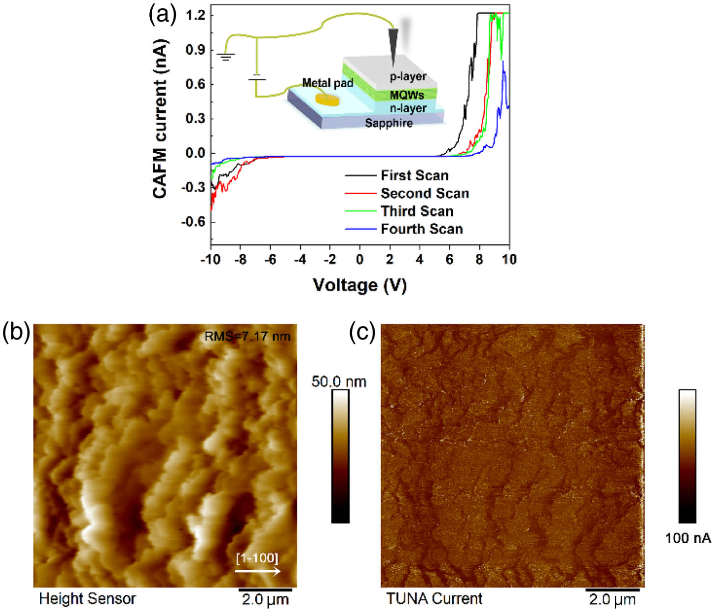
    Fig. 1. (a) Schematic setup of CAFM and four consecutive IV curves during the scans; (b) typical surface morphology of UV LED grown on a 1° misoriented sapphire substrate; and (c) corresponding current distribution map under forward bias of +7  V.
    (a) Top view SEM image of the surface of UV LED; (b) zoom-in view image near the step edge as indicated by the green box and (c) corresponding ECCI graph.
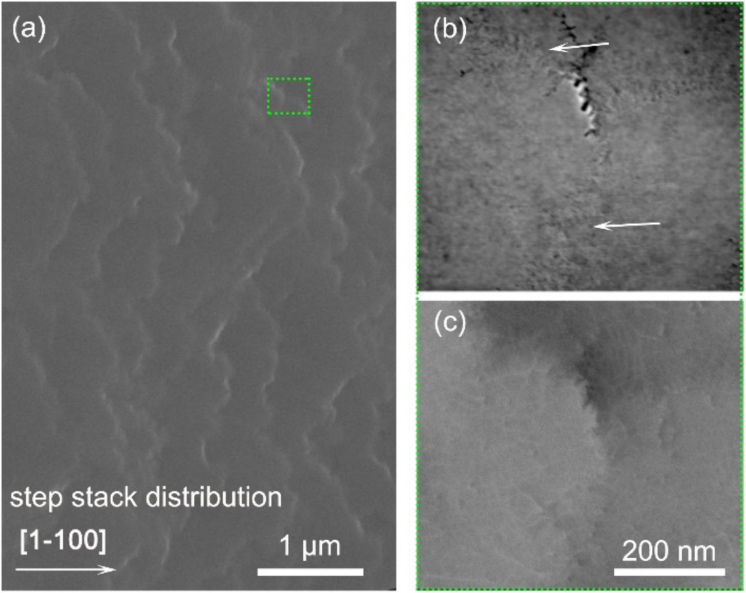
    Fig. 2. (a) Top view SEM image of the surface of UV LED; (b) zoom-in view image near the step edge as indicated by the green box and (c) corresponding ECCI graph.
    (a) Cross-sectional g=[0002] and (b) g=[11−20] dark-field TEM images under two-beam conditions for UV LED grown on a 1° misoriented sapphire substrate; (c) cross-sectional image of the MQW and corresponding Ga EDS mapping near the step edge; (d) zoom-in view of the MQW regions.
    Fig. 3. (a) Cross-sectional g=[0002] and (b) g=[1120] dark-field TEM images under two-beam conditions for UV LED grown on a 1° misoriented sapphire substrate; (c) cross-sectional image of the MQW and corresponding Ga EDS mapping near the step edge; (d) zoom-in view of the MQW regions.
    (a) RT PL spectrum of UV LED grown on a 1° misoriented sapphire substrate; (b) PL spectra of UV LED under RT and LT; (c) RT EL spectrum of the same sample under current injection of 200 mA; (d) EL spectra under injection currents ranging from 50 to 300 mA.
    Fig. 4. (a) RT PL spectrum of UV LED grown on a 1° misoriented sapphire substrate; (b) PL spectra of UV LED under RT and LT; (c) RT EL spectrum of the same sample under current injection of 200 mA; (d) EL spectra under injection currents ranging from 50 to 300 mA.
    (a) I-V curve; (b) EL spectra under different injection currents from 5 to 80 mA; (c) light output power and estimated EQE as functions of injection current.
    Fig. 5. (a) I-V curve; (b) EL spectra under different injection currents from 5 to 80 mA; (c) light output power and estimated EQE as functions of injection current.
    (a) Schematic structure and composition distribution of a UV LED with single QW in the simulation; (b) the distribution of radiative recombination rate; and (c) total current distribution; (d) the energy band structure and (e) distribution of carrier concentration of the flat and inclined active region, respectively. EC and HC stand for electron concentration and hole concentration. (f) EL spectra of the UV LED under different current densities.
    Fig. 6. (a) Schematic structure and composition distribution of a UV LED with single QW in the simulation; (b) the distribution of radiative recombination rate; and (c) total current distribution; (d) the energy band structure and (e) distribution of carrier concentration of the flat and inclined active region, respectively. EC and HC stand for electron concentration and hole concentration. (f) EL spectra of the UV LED under different current densities.
    Proposed 3D schematic band diagram of the active region of the UV LED across the step-bunched region.
    Fig. 7. Proposed 3D schematic band diagram of the active region of the UV LED across the step-bunched region.
    Houqiang Xu, Jiean Jiang, Li Chen, Jason Hoo, Long Yan, Shiping Guo, Cai Shen, Yanping Wei, Hua Shao, Zi-Hui Zhang, Wei Guo, Jichun Ye. Direct demonstration of carrier distribution and recombination within step-bunched UV-LEDs[J]. Photonics Research, 2021, 9(5): 764
    Download Citation