
Houqiang Xu, Jiean Jiang, Li Chen, Jason Hoo, Long Yan, Shiping Guo, Cai Shen, Yanping Wei, Hua Shao, Zi-Hui Zhang, Wei Guo, Jichun Ye. Direct demonstration of carrier distribution and recombination within step-bunched UV-LEDs[J]. Photonics Research, 2021, 9(5): 764
- Photonics Research
- Vol. 9, Issue 5, 764 (2021)
Abstract
1. INTRODUCTION
AlGaN-based ultraviolet light-emitting diodes (UV LEDs), with the advantages of compact structure, long lifetime, and controllable wavelength, are promising in numerous applications, such as air/water sterilization [1], surface disinfection [2], plant growth [3], and the detection of biochemical agents [1,4,5]. However, the development of AlGaN-based UV LEDs is still in its infancy compared to InGaN-based blue and green LEDs, owing to various scientific and technical challenges, such as inferior crystal quality [6], low doping efficiency of high Al composition p-type layers [7], poor light extraction efficiency due to dominant TM light polarization [8], and UV light absorption by p-GaN and metal contacts [9]. As a matter of fact, the widely reported external quantum efficiencies (EQEs) of AlGaN-based UV LEDs are mostly below 5% [10–13].
Internal quantum efficiency (IQE) is one of the most important factors contributing to the EQE of UV LEDs. Ban
Despite progress made in the fabrication of UV LEDs on misoriented substrates, the physics of carrier transportation and recombination in the active regions is still poorly understood. In our previous work, it was reported that radiative recombination center formed in the step edge area with the support of -cathodoluminescence (CL) characterization [15]. Kojima
Sign up for Photonics Research TOC. Get the latest issue of Photonics Research delivered right to you!Sign up now
In this work, the dependence of current distribution on the surface morphology in the sub-300 nm emission of UV-LEDs grown on misoriented sapphire substrate was investigated in detail. It is demonstrated that as forward bias increases, the current flows through the step edge first, and then expands to adjacent regions. The macro-step structure was also modeled and simulated according to transmission electron microscopy observations. Current paths are formed in the step edges owing to Ga enrichment. Further investigations found that the IQWs have better carrier confinement due to both smaller bandgap and spontaneous polarization compared to adjacent flat QWs. This comprehensive study clearly illustrates that a UV LED grown on misoriented substrate is only one of the many techniques to achieve phase separation and carrier localization, which provides a new perspective in the realization of high-efficiency UV emitters.
2. EXPERIMENT SECTION
AlGaN-based UV LEDs were grown on 2-inch -plane sapphire substrates with an approximate 1° misorientation angle toward the plane using an AMEC Prismo MOCVD reactor in ambient. Trimethylaluminum, trimethylgallium, and ammonia () were used as precursors of Al, Ga, and N, respectively. Hydrogen () and nitrogen () were used as the carrier gases. Initially, a 20 nm thick low-temperature (LT) AlN nucleation layer (NL) was deposited on the sapphire substrate at 850°C. A 2.8 μm high-temperature (HT) AlN template was subsequently grown under 1250°C, followed by 50 pairs of AlN/AlGaN superlattices used as dislocation filters. Then, a 2 μm Si-doped n- contact layer was deposited. Afterwards, four pairs of MQWs were grown under 1050°C. A 20 nm p- electron barrier layer (EBL), 50 nm p- layer, and 50 nm -GaN contact layer were subsequently deposited. Surface morphologies and spatially resolved current distributions of the UV LEDs were characterized by a Veeco Dimension 3100V conductive atomic force microscope (CAFM) in contact mode with a Pt-coated Si probe. Crystalline qualities were analyzed using a point-focused high-resolution X-ray (Cu Ka1) diffractometer (HRXRD, Bruker D8 DISCOVER) equipped with a four-bounce symmetric Ge (220) monochromator. PL studies were performed using a Coherent Ar-F (193 nm) excimer laser at pumping power of , collected by a Horiba iHR550 spectrometer. Electroluminescence (EL) was analyzed by a Keithley 4200-SCS semiconductor characterization system. Electron channeling contrast imaging (ECCI) investigation was performed using a Verios G4 UC characterization system with voltage of 20 kV. Transmission electron microscopy (TEM) samples were prepared using an Helios dual-beam focused ion beam scanning electron microscope system with a Ga ion source. Thicknesses of MQWs and dislocation distributions were characterized by an FEI probe-corrected Titan high-angle annular dark-field imaging-scanning transmission electron microscopy (HAADF-STEM) system operated at an acceleration voltage of 300 kV. All measurements were performed at room temperature (RT).
3. RESULTS AND DISCUSSION
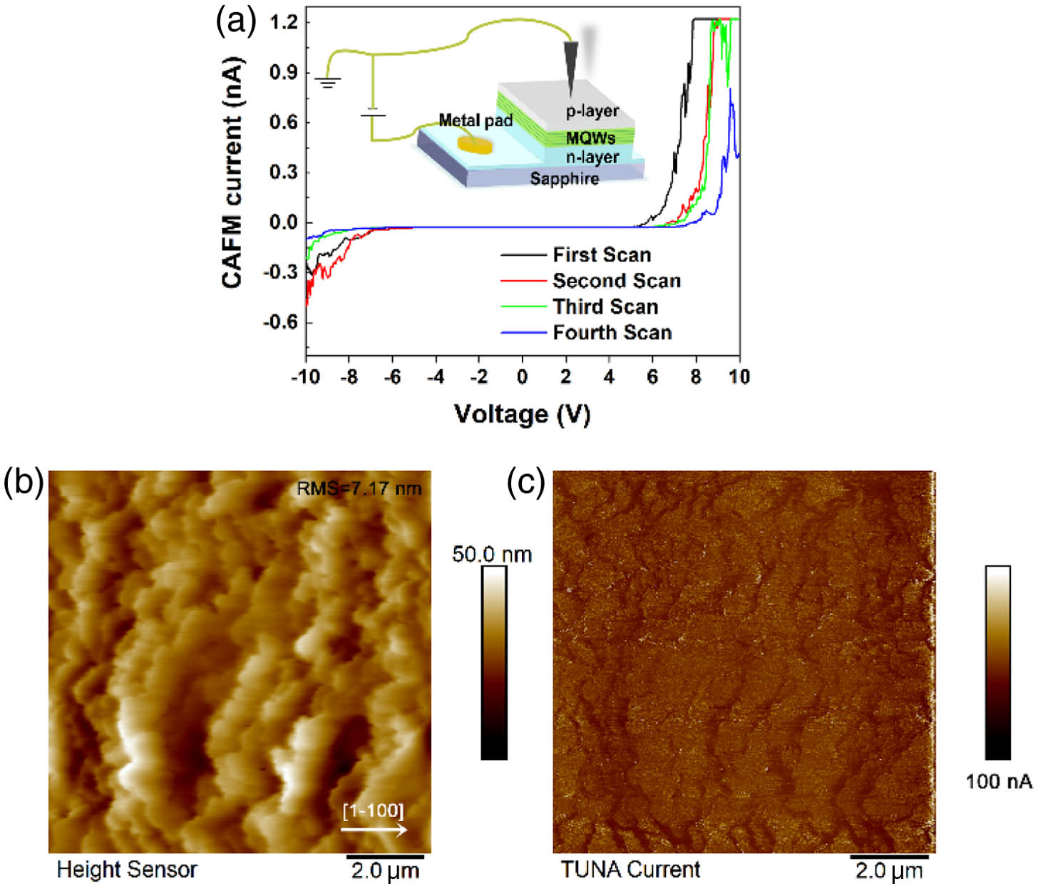
Figure 1.(a) Schematic setup of CAFM and four consecutive
The current-voltage (I-V) curves shown in Fig. 1(a) represent a local electrical behavior near the step edge within the voltage range of to . The I-V characterization was performed consecutively 4 times. When forward voltage bias (0–10 V) was applied to the surface, even though the turn-on voltage increases with the scan proceeding, the local current becomes saturated at higher bias, indicating a stable current pathway. However, when UV LED is under reverse bias (), the reverse current reduces as the number of scans increases and finally becomes negligible. Prior CAFM studies show that dislocations may serve as channels for large and stable reverse-bias leakage current [24]. This is in contrast with the observation in this work, suggesting that the local current distributions in the UV LEDs are not associated with dislocations. From the surface morphology image shown in Fig. 1(b), large numbers of step bunching are formed on the surface. Spradlin
![]()
Figure 2.(a) Top view SEM image of the surface of UV LED; (b) zoom-in view image near the step edge as indicated by the green box and (c) corresponding ECCI graph.
![]()
Figure 3.(a) Cross-sectional
Figure 3(d) shows the zoom-in view of the MQWs near the step edge. The orientation and thickness of Ga-deficient and Ga-rich layers of the sample can be distinguished by the dark and bright contrast, respectively [30]. The MQW is 1° tilted relative to the (0001) crystallographic plane, as indicated by the white dashed line in Fig. 3(d), in accordance with the substrate misorientation angle of . Thickness expansion or even twist of the QWs can be observed at the edge. The width of the AlGaN QWs grown on the flat surface is , while the width slightly expands to near the step edges. Even though the exact composition difference in the step edges is not known, there is no denying that thickness and composition fluctuation will result in lower bandgap. This would in turn lead to the different electrical and optical behaviors of the UV LEDs.
![]()
Figure 4.(a) RT PL spectrum of UV LED grown on a 1° misoriented sapphire substrate; (b) PL spectra of UV LED under RT and LT; (c) RT EL spectrum of the same sample under current injection of 200 mA; (d) EL spectra under injection currents ranging from 50 to 300 mA.
Figure 4(c) illustrates the EL spectrum of the UV LED under an injection current of 200 mA. There are also two emission peaks located at wavelengths of 287 and 298 nm. Due to strong UV absorption in the p-GaN contact layer, PL characterization was performed under high pumping power, leading to a strong band filling effect and thus blueshift of the peak position. More importantly, during optical pumping, both Ga-rich and Ga-deficient regions are uniformly excited. On the contrary, under electrical injection condition, photons mostly come from Ga-rich regions in UV LEDs due to the carrier localization effect. As a consequence, PL exhibits a shorter emission wavelength compared to EL. In addition, note that the intensity of the longer-wavelength emission peak is stronger than that of the shorter-wavelength one in Fig. 4(c). This is in contrast with the PL spectrum, suggesting that under current injection, carriers are more inclined to pass through the IQW region, where the carrier localization effect is enhanced. Note that from the CAFM result in Fig. 1, current is mainly localized in the step edges when the device is turned on, confirming that EL characterization is highly dependent on the surface morphology. To demonstrate this hypothesis, EL spectra under various injection currents from 50 to 300 mA are shown in Fig. 4(d). A shorter-wavelength peak can barely be seen under the low injection current, while as the current injection increases, the intensity of the shorter-wavelength emission peak increases significantly. This can be ascribed to the saturation of the current paths at the step edges, which will be further discussed later on.
![]()
Figure 5.(a)
![]()
Figure 6.(a) Schematic structure and composition distribution of a UV LED with single QW in the simulation; (b) the distribution of radiative recombination rate; and (c) total current distribution; (d) the energy band structure and (e) distribution of carrier concentration of the flat and inclined active region, respectively. EC and HC stand for electron concentration and hole concentration. (f) EL spectra of the UV LED under different current densities.
Figure 6(f) shows the simulated EL spectra under the injection current densities of , , and . Single peak emission at 290 nm is observed under , while double peaks appear when the current increases. Note that the current is mainly concentrated in the step edge when a relatively low current density of at the bias of is applied on the sample [Fig. 6(c)]. When the current density increases to , current spreads to the periphery of the step edge region, as shown in the inset in Fig. 6(c). This is clearly demonstrated by the occurrence of a high-energy side peak from the simulation result. Therefore, under the condition of high current density injection, carrier delocalization occurs, and the current distribution becomes more uniform.
![]()
Figure 7.Proposed 3D schematic band diagram of the active region of the UV LED across the step-bunched region.
Interestingly, step-bunching-induced Ga phase separation not only appears in AlGaN grown on high misorientation sapphire. Similar phenomena have been observed in MQWs grown on low misorientation substrate or even on-axis sapphires, where nitride thin films exhibit step-flow growth morphology [6,17,32]. Carrier localization has always been a common observation in III-nitrides, especially InGaN. Currents prefer to reside in the potential minima. The investigations shown in this work are in fact valid for all ternary III-V semiconductor systems exhibiting phase separation, including III-arsenide. Understanding the carrier transport and recombination behaviors in such thin films can greatly help us to improve the performance of III-V semiconductor devices.
4. CONCLUSION
In summary, a sub-300 nm UVB LED with IQE of 63% and EQE of 1.23% was designed and fabricated on a 1° misoriented sapphire substrate. Direct evidence on carrier transportation and recombination on step-bunched surface of UV-LED was provided. The current distribution strongly follows the surface morphology of the thin film. Top view ECCI and cross-sectional HAADF-STEM demonstrated that these current paths are not associated with threading dislocations, but rather are related to the step edges with Ga-rich potential minima. This structure was further modeled and simulated by solving the Poisson equations and carrier transport equations. An efficient recombination center is formed in the IQWs owing to higher carrier concentration and larger radiative recombination rates. Finally, a schematic diagram of a 3D energy band structure of the active region of the UV LED across the step edges was proposed.
Acknowledgment
Acknowledgment. The authors appreciate the technical support from Nano Fabrication Facility, Platform for Characterization & Test in Ningbo Institute of Materials Technology and Engineering, CAS.
References
[1] C. Zhou, A. Ghods, V. G. Saravade, P. V. Patel, K. L. Yunghans, C. Ferguson, Y. Feng, B. Kucukgok, N. Lu, I. T. Ferguson. Review—the current and emerging applications of the III-nitrides. ECS J. Solid State Sci. Technol., 6, Q149-Q156(2017).
[2] M. Kneissl, J. Rass. III-Nitride Ultraviolet Emitters: Technology and Applications(2016).
[3] S. Matsuura, S. Ishikura. Suppression of tomato mosaic virus disease in tomato plants by deep ultraviolet irradiation using light-emitting diodes. Lett. Appl. Microbiol., 59, 457-463(2014).
[4] P. J. Hargis, T. J. Sobering, G. C. Tisone, J. Wagner, S. A. Young, R. J. Radloff. Ultraviolet fluorescence identification of protein, DNA, and bacteria. Proc. SPIE, 2366, 147-153(1995).
[5] K. Song, M. Mohseni, F. Taghipour. Application of ultraviolet light-emitting diodes (UV-LEDs) for water disinfection: a review. Water Res., 94, 341-349(2016).
[6] M. X. Wang, F. J. Xu, N. Xie, Y. H. Sun, B. Y. Liu, Z. X. Qin, X. Q. Wang, B. Shen. Crystal quality evolution of AlN films via high temperature annealing under ambient N2 conditions. CrystEngComm, 20, 6613-6617(2018).
[7] S. Zlotnik, J. Sitek, K. Rosiński, P. P. Michałowski, J. Gaca, M. Wójcik, M. Rudziński. Growth and thermal annealing for acceptor activation of p-type (Al)GaN epitaxial structures: technological challenges and risks. Appl. Surf. Sci., 488, 688-695(2019).
[8] H. Xu, H. Long, J. Jiang, M. Sheikhi, L. Li, W. Guo, J. Dai, C. Chen, J. Ye. Strain modulated nanostructure patterned AlGaN-based deep ultraviolet multiple-quantum-wells for polarization control and light extraction efficiency enhancement. Nanotechnology, 30, 435202(2019).
[9] N. Maeda, H. Hirayama. Realization of high-efficiency deep-UV LEDs using transparent p-AlGaN contact layer. Phys. Status Solidi C, 10, 1521-1524(2013).
[10] N. Susilo, S. Hagedorn, D. Jaeger, H. Miyake, U. Zeimer, C. Reich, B. Neuschulz, L. Sulmoni, M. Guttmann, F. Mehnke, C. Kuhn, T. Wernicke, M. Weyers, M. Kneissl. AlGaN-based deep UV LEDs grown on sputtered and high temperature annealed AIN/sapphire. Appl. Phys. Lett., 112, 041110(2018).
[11] M. A. Khan, N. Maeda, M. Jo, Y. Akamatsu, R. Tanabe, Y. Yamada, H. Hirayama. 13 mW operation of a 295–310 nm AlGaN UV-B LED with a p-AlGaN transparent contact layer for real world applications. J. Mater. Chem., 7, 143-152(2019).
[12] M. Kneissl, T. Y. Seong, J. Han, H. Amano. The emergence and prospects of deep-ultraviolet light-emitting diode technologies. Nat. Photonics, 13, 233-244(2019).
[13] P. Dong, J. Yan, J. Wang, Y. Zhang, C. Geng, T. Wei, P. Cong, Y. Zhang, J. Zeng, Y. Tian, L. Sun, Q. Yan, J. Li, S. Fan, Z. Qin. 282-nm AlGaN-based deep ultraviolet light-emitting diodes with improved performance on nano-patterned sapphire substrates. Appl. Phys. Lett., 102, 241113(2013).
[14] K. Ban, J. Yamamoto, K. Takeda, K. Ide, M. Iwaya, T. Takeuchi, S. Kamiyama, I. Akasaki, H. Amano. Internal quantum efficiency of whole-composition-range AlGaN multiquantum wells. Appl. Phys. Express, 4, 052101(2011).
[15] H. Xu, J. A. Jiang, M. Sheikhi, Z. Chen, J. Hoo, S. Guo, W. Guo, H. Sun, J. Ye. Single peak deep ultraviolet emission and high internal quantum efficiency in AlGaN quantum wells grown on large miscut sapphire substrates. Superlattices Microstruct., 129, 20-27(2019).
[16] H. Sun, S. Mitra, R. C. Subedi, Y. Zhang, W. Guo, J. Ye, M. K. Shakfa, T. K. Ng, B. S. Ooi, I. S. Roqan, Z. Zhang, J. Dai, C. Chen, S. Long. Unambiguously enhanced ultraviolet luminescence of AlGaN wavy quantum well structures grown on large misoriented sapphire substrate. Adv. Funct. Mater., 29, 1905445(2019).
[17] M. Hou, Z. Qin, L. Zhang, T. Han, M. Wang, F. Xu, X. Wang, T. Yu, Z. Fang, B. J. S. Shen. Excitonic localization at macrostep edges in AlGaN/AlGaN multiple quantum wells. Superlattices Microstruct., 104, 397-401(2017).
[18] H. Kojima, T. Ogasawara, M. Kim, Y. Saito, K. Iida, N. Koide, T. Takeuchi, M. Iwaya, S. Kamiyama, I. Akasaki. Sapphire substrate off-angle and off-direction dependences on characteristics of AlGaN-based deep ultraviolet light-emitting diodes. Jpn. J. Appl. Phys., 58, sc1025(2019).
[19] T. Kolbe, A. Knauer, J. Enslin, S. Hagedorn, A. Mogilatenko, T. Wernicke, M. Kneissl, M. Weyers. Influence of substrate off-cut angle on the performance of 310 nm light emitting diodes. J. Cryst. Growth, 526, 125241(2019).
[20] Y. H. Sun, F. J. Xu, N. Xie, J. M. Wang, N. Zhang, J. Lang, B. Y. Liu, X. Z. Fang, L. B. Wang, W. K. Ge, X. N. Kang, Z. X. Qin, X. L. Yang, X. Q. Wang, B. Shen. Controlled bunching approach for achieving high efficiency active region in AlGaN-based deep ultraviolet light-emitting devices with dual-band emission. Appl. Phys. Lett., 116, 212102(2020).
[21] Y. Nagasawa, R. Sugie, K. Kojima, A. Hirano, M. Ippommatsu, Y. Honda, H. Amano, I. Akasaki, S. F. Chichibu. Two-dimensional analysis of the nonuniform quantum yields of multiple quantum wells for AlGaN-based deep-ultraviolet LEDs grown on AlN templates with dense macrosteps using cathodoluminescence spectroscopy. J. Appl. Phys., 126, 215703(2019).
[22] M. Hayakawa, S. Ichikawa, M. Funato, Y. Kawakami. Al
[23] K. Jiang, X. Sun, J. Ben, Z. Shi, Y. Jia, Y. Wu, C. Kai, Y. Wang, D. Li. Suppressing the compositional nonuniformity of AlGaN grown on HVPE-AlN template with large macro-steps. CrystEngComm, 21, 4864-4873(2019).
[24] D. Liu, S. J. Cho, H. Zhang, C. Carlos, R. Kalapala, J. Park, J. Kim, R. Dalmau, J. Gong, B. Moody, X. Dong, J. D. Albrecht, W. Zhou, Z. Ma. Influences of screw dislocations on electroluminescence of AlGaN/AlN-based UVC LEDs. AIP Adv., 9, 085128(2019).
[25] J. Spradlin, S. Dogan, J. Xie, R. J. Molnar, A. A. Baski, H. Morkoc. Investigation of forward and reverse current conduction in GaN films by conductive atomic force microscopy. Appl. Phys. Lett., 84, 4150-4152(2004).
[26] S. Walde, S. Hagedorn, P.-M. Coulon, A. Mogilatenko, C. Netzel, J. Weinrich, N. Susilo, E. Ziffer, L. Matiwe, C. Hartmann, G. Kusch, A. Alasmari, G. Naresh-Kumar, C. Trager-Cowan, T. Wernicke, T. Straubinger, M. Bickermann, R. W. Martin, P. A. Shields, M. Kneissl, M. Weyers. AlN overgrowth of nano-pillar-patterned sapphire with different offcut angle by metalorganic vapor phase epitaxy. J. Cryst. Growth, 531, 125343(2020).
[27] N. Susilo, J. Enslin, L. Sulmoni, M. Guttmann, U. Zeimer, T. Wernicke, M. Weyers, M. Kneissl. Effect of the GaN:Mg contact layer on the light-output and current-voltage characteristic of UVB LEDs. Phys. Status Solidi A, 215, 1700643(2018).
[28] F. Ponce, D. Cherns, W. T. Young, J. W. Steeds. Characterization of dislocations in GaN by transmission electron diffraction and microscopy techniques. Appl. Phys. Lett., 69, 770-772(1996).
[29] K. Kojima, Y. Nagasawa, A. Hirano, M. Ippommatsu, Y. Honda, H. Amano, I. Akasaki, S. F. Chichibu. Carrier localization structure combined with current micropaths in AlGaN quantum wells grown on an AlN template with macrosteps. Appl. Phys. Lett., 114, 011102(2019).
[30] W. Guo, H. Sun, B. Torre, J. Q. Li, M. Sheiki, J. Jiang, H. Li, S. Guo, K. Li, R. Lin, A. Giugni, E. D. Fabrizio, X. Li, J. Ye. Lateral polarity structure of AlGaN quantum wells: a promising approach to enhancing the ultraviolet luminescence. Adv. Funct. Mater., 28, 1802395(2018).
[31] H. Masui, S. Nakamura. Nonpolar and semipolar orientations: material growth and properties. Mater. Sci. Forum, 590, 211-232(2008).
[32] J. Yan, J. Wang, Y. Zhang, P. Cong, L. Sun, Y. Tian, C. Zhao, J. Li. AlGaN-based deep-ultraviolet light-emitting diodes grown on high-quality AlN template using MOVPE. J. Cryst. Growth, 414, 254-257(2015).

Set citation alerts for the article
Please enter your email address
© Copyright 2018-2021 | Chinese Laser Press. All Rights Reserved 沪ICP备15018463号-20