Abstract
The self-formation of periodic subwavelength ripples by linear polarized femtosecond laser scanning planar and non-planar tungsten targets on the employed laser wavelength, scanning speed, and energy fluence are examined systematically. The results show that, for a certain laser wavelength, the scanning conditions have no obvious effect to the morphological features of grating structures in the threshold range of laser fluence. The spatial structured period of gratings can be self-consistently interpreted by recently presented physical model of surface two-plasmon resonance. The subwavelength structures on cylindrical surface would be a good method to realize unique surface functions on complex surface of micro-devices.Micro/nanostructures on a natural biology surface with unique surface characteristics can help them to adapt to the natural environment. For example, the micro/nanostructures on a lotus leaf surface can make themselves be of superhydrophobicity and have excellent self-cleaning properties[1,2]. Dragonfly wings covered with a large number of nanoscale structuring mastoids and microsculptures can enhance the surface hydrophobicity of the wings, allowing them to remain uncontaminated under the environments of rain, fog, dew, dust, etc., and thus ensures their flight safety[3,4]. With advancements of femtosecond (fs) laser technology, fs-laser micromachining as a precise machining process with high resolution has gained considerable attention due to the wide range of nearly all types of materials[5] such as metals[6–10], semiconductors[11–14], polymers[15–17], and dielectric materials[18–20]. The induced structure sizes are from the nanometer to micrometer scales[6,11,21–23], the spatial structured patterns involve randomness[9] and periodicity[8,10,11,16,24–27], and the spatial structured period (SSP) is the subwavelength scale or even shorter than half of the laser wavelength[5,23,25,26]. These subwavelength nanostructures provide many unique properties leading to extensive applications in nano-optics, electronic devices, material physics, and chemical surface engineering, etc., and therefore have been eye-catching.
In order to achieve a controllable fabrication for the requirements of variant applications most efforts have focused on determining the formation mechanism of these characteristic subwavelength structures, such as the interference between a surface plasmon and incident laser[12,27], surface plasmon effects[28–30], initial surface roughness[24,31,32], kinds of heating[21,33], resonant Mie scattering[34,35], and so on. Another typical mechanism was reported by Sakabe et al.[36] in which the parametric decay resulting from stimulated Raman scattering (SRS) was suggested as a logical physical mechanism and an expression to evaluate the SSP of ripples was presented. Nevertheless, the SRS process cannot fully interpret how the generation of a surface-plasma wave induces periodic structures, as mentioned by Okamuro et al.[37]. Thus, the inferences for the intrinsic dependence of structure formation are still limited in qualitative hypotheses, especially for the self-formation of an SSP much shorter than half of the employed fs-laser wavelength (i.e., ), and there is not a self-consistent interpretation from the physical mechanism so far.
Recently, we proposed surface two-plasmon resonance (STPR) generated in the ultrafast interaction of a fs-laser pulse with a surface plasmon produced on a target surface that gives birth to periodic subwavelength ripple structures[26]. The STPR results from nonlinear coupling of three waves: a fs-laser light wave (pump wave) and two surface plasmon waves (i.e., Langmuir waves). When a metal surface is exposed to a fs-laser pulse normally, an ionized electron plasma sheet (inhomogeneous density) is formed rapidly and two plasmon waves in opposite directions along the target surface are immediately excited due to electrons oscillating in the laser’s electric field. Once the phase relations of the three waves, wave vectors and frequencies, are matched due to an electron density perturbation, the phase-locked STPR is steadily driven just like a traditional pendulum. Consequently, a periodic electrostatic field between the phase-locked STPR wave (electronegative) and ions (electropositive) bound in the target surface is stably formed and then Coulomb ablation occurs on the target surface when the electrostatic potential exceeds the binding energy of the target atom. If we suitably control the employed laser fluence so that the electrostatic potential exceeds the atomic binding energy only at peaks of over-dense electrons in the STPR wave, the wave crest ablation takes place only at the peak corresponding locations and the wave pattern of the STPR is homoplastically “carved” on the target surface (removal) with SSP or even . The wavelength of the grating SSP derived from the STPR model[26] is where is the number density of electrons in the skin layer of the incident laser penetrating the sample surface and the units of , , and are in μm, , and , respectively. It indicates that the SSP of the self-formed gratings strongly depends on the laser wavelength and the properties of the target materials.
Sign up for Chinese Optics Letters TOC. Get the latest issue of Chinese Optics Letters delivered right to you!Sign up now
In this work, subwavelength nanoripples were fabricated by a fs-laser scanning a tungsten (W) metal surface with different processing parameters by virtue of which the large areas of the well-regulated nanogratings were quickly formed successfully on planar and nonplanar surfaces. The results can be interpreted well by the STPR model.
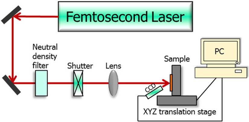
The experimental setup, shown in Fig. 1, is equipped with a commercial fs-laser system with a pulse duration of and 3.5 mJ/pulse, a central wavelength of , and a 1 kHz repetitive rate. The polished W metal sample was placed on a three-dimensional motorized precision translation stage controlled by a computer program. The horizontally polarized fs-laser pulse was normally focused on the sample surface through a 200 mm lens and the focused spot diameter was about 60 μm. By controlling the translation stage motion at a certain speed and retaining the incident laser beam immobility, orderly ripples can be obtained quickly; moving the stage equivalently means fs-laser beam scanning the sample surface at the same but retrorse speed. The CCD is used here to monitor the structuring process synchronously. To get optimized processing parameters, systematic experiments were performed.

Figure 1.Schematic diagram for fs-laser scanning on a planar target in the experiment.
First, the subwavelength ripples on the planar target surface at wavelengths and 800 nm, were fabricated by fs-laser scanning. Here, a beta-barium borate (BBO) frequency doubling crystal and a bandpass filter with a 400 nm center wavelength were used for generating a 400 nm wavelength laser pulse. The fs-laser scanning fluence and scanning velocity were used. The scanning electron microscope (SEM) images in Fig. 2 show the SSPs of grating structures from which we can find that the average SSPs induced by a 400 nm laser wavelength are [, see Fig. 2(a)] and the average SSPs induced by a 800 nm laser wavelength are [, see Fig. 2(b)].
Figure 2.SEM images of grating structures on a W metal target induced by a fs-laser with wavelengths of (a) and (b) .
Second, the subwavelength ripples fabricated by different laser scanning speeds were performed on the planar target. The W sample surface was irradiated by an 800 nm wavelength laser scanning with a fluence of at speeds of 0.94, 1.10, 1.25, 1.56, and 1.88 mm/s, respectively. Figure 3 shows the SEM images of the self-formed grating structure on the sample surface. The average SSP of the gratings measured is about () for different scanning speeds, which shows a small deviation.
Figure 3.SEM images of grating structures formed by an 800 nm wavelength laser with an energy fluence at scanning speeds of (a) , (b) , (c) , and (d) , respectively.
Further, one can find from Fig. 4 that the contribution of the scanning speed to the ablation depth (depth of gratings) is substantive. The blue dots denote the experimental values and the red dashed line is the corresponding fitted curve to the experimental values and gives . It distinctly exhibits an exponential decay with the increase of the scanning speed and demonstrates that a higher scanning speed is corresponding to a lower laser energy absorption of the material surface. To highlight the change of the ablated depth in detail, the curve measured by an atomic force microscope (AFM) in the direction perpendicular to the gratings at a scanning speed of is inserted in Fig. 4, which shows a uniform evolution and gives an average depth of 226 nm. Thus, we conclude that the contribution of the scanning speed to the grating SSP is inconspicuous in an applicable velocity range and is substantive to the ablating depth.
Figure 4.Ablation depth of gratings versus the laser scanning speed for an 800 nm wavelength and experiment, where the red dashed line is the corresponding fitted curve and the depth change measured by an AFM at a constant scanning speed and the laser fluence is inserted at top right corner.
Third, the subwavelength ripples were fabricated on a planar target by different laser fluences. The W sample surface was scanned by a fs-laser beam at a speed of 1.25 mm/s with fluences of , , , , and , respectively. Figure 5 shows the SEM images of gratings formed by the 800 nm wavelength laser at different scanning speeds. The average SSP of gratings was measured at (), which also shows a small deviation. This demonstrates that the contribution of thr laser fluence to the SSPs is relatively weak () in the fluence range of , which also can be well explained and agrees with the theoretical prediction and experimental observations in Ref. [26]. By further diagnosis we find that laser fluence mainly affects the ablating depth of the gratings and the stress crack appears on the structured surface as the fluence rises to , which is seen from Fig. 5(d). The dependency relationship between the scanning energy fluence and the ablated depth of gratings is shown in Fig. 6 in which the blue dots denote the observations and the red dashed line is the corresponding fitting curve expressed as . One can see that the dependence displays an exponential increase with the energy fluence because obviously the higher the fluence used the more the material surface absorbs energy and thus the deeper the surface is ablated by the laser beam. The AFM curve of the ablated depth is inserted at the lower right corner in Fig. 6, which exhibits a uniform change in the constant scanning speed and the laser fluence. Therefore, to obtain the expected and feasible structuring patterns, we need to moderately choose the employed laser wavelength, energy fluence, and scanning speed.
Figure 5.SEM images of grating structures formed by a 800 nm wavelength laser at the scanning speed of 1.25 mm/s with energy fluences of (a) , (b) , (c) , and (d) .
Figure 6.Ablation depth of gratings versus the laser fluence for a 800 nm laser wavelength and 1.25 mm/s scanning speed. The meanings of the other curves and symbols are analogous to Fig. 4.
Based on the above experimental results and experience, we examined the holistic surface topography of grating structures formed on the W planar target by the fast laser scanning of a large area along the direction of laser polarization for which we optimally chose the scanning speed of 1.2 mm/s and the laser fluence of . The schematic diagram for subwavelength ripple fabrication by the fast scanning of a fs-laser beam is shown in Fig. 7(a), where the blue area is the zone scanned by single-pass laser scanning and the saffron yellow area is the overlapped zone due to the back and forth scanning way of laser beams. The single-pass scanning width is considered to be approximately the same as the spot diameter () and the overlapped width due to the back and forth (double-pass) scanning is adjustable. In this experiment, the overlapped width was adjusted from 0 to 10 μm and the SEM images of the topography produced by single-pass and double-pass laser scanning are shown in Figs. 7(b)–7(d). One can see, from Fig. 7(b), that a neat orderly grating structure on the wavelength scale () is self-formed by single-pass laser scanning. Interestingly, when the back and forth scanning method is used, the gratings still retain their homogeneity and regularity satisfactorily whether there is an overlap or not between back and forth laser scanning beams, which can be seen from the amplified SEM images on the right sides of Figs. 7(c) and 7(d). By this method, a grating area of was quickly achieved within 210 s.
Figure 7.(a) Schematic diagram for grating structure fabrication by laser scanning, where the blue area is the zone formed by single-pass laser scanning and the saffron yellow area is the overlapped zone due to back and forth laser scanning. The SEM images are grating structures obtained in different scanning zones by (b) single-pass scanning, (c) back and forth scanning with a gap between scanning beams, and (d) back and forth scanning with a 10 μm overlap between scanning beams.
In practical applications, to achieve some special functions one generally needs to implement the designed micro- or nanostructures on the surfaces of various irregular shapes such as that of actual devices or components. Thus, it is very important to efficiently fabricate the required structures on nonplanar material surfaces. We make an effort to extend the planar surface structuring of the laser scanning to cylindrical surface structuring for which the experimental setup stayed the same as Fig. 1 except the translation stage was replaced by a motorized rotating stage. In the experiment, the laser with a fluence of was focused on the surface of the cylindrical W target by an lens and the rotation speed of the target (the cylinder radii are 1, 3, and 5 mm, respectively) loaded on the rotating stage was controlled at 0.24 rad/s circle-by-circle. The overlapped width of two circles scanning a round cylindrical path was also selected to 10 μm and the scanning direction was still in the polarization direction of the laser electric field, as shown in Fig. 8(a). One can obviously see that the self-formed subwavelength grating structures on the scanned cylindrical target surface still retain uniformity and regularity in morphology, which is displayed directly in Figs. 8(c) and 8(d), and is the same as the beautiful reflection picture of white light shown in Fig. 8(b). Further experiments show that, when the height () of the cambered surface cap irradiated by the laser pulse is less than a Rayleigh length (, half the confocal parameter) i.e., ( is the focus spot radius), as shown in Fig. 9, the uniformity of the structured period is maintained. Therefore, the result is straightforward because the effect of the cambered surface on the self-formation of grating structures is negligible if the focal depth of lthe aser beam is much larger than the height of the cylindrical curvature covered by the focal spot.
Figure 8.(a) Schematic diagram for grating structure fabrication by laser scanning circle-by-circle, where the blue area is the zone formed by single-pass scanning and the saffron yellow area is the zone overlapped by two scanning circles, (b) the scanned cylindrical target with a radius of 5 mm on which the grating effect appears, and (c) and (d) the SEM images of self-formed grating structures in the zone overlapped by two scanning circles.
Figure 9.Schematic diagram for the self-formation of ripple structures on a nonplanar surface by a fs-laser pulse.
In conclusion, the periodic subwavelength grating structures on planar and cylindrical target surfaces formed by linearly polarized fs laser scanning are systematically investigated experimentally. The results indicate that, whether for planar or cylindrical targets, the SSP is mainly dependent on the employed laser wavelength as well as weakly by material properties, the orientation of the gratings is perpendicular to the direction of laser polarization and independent of the scanning direction, which are satisfactorily foretold by the present STPR model. The ablated depth of the grating structures is directly dominated by the scanning speed and energy fluence of the laser beam, in terms of which the depths exponentially increases with the laser fluence and exponentially decays with the scanning speed. In morphology, the grating structures in the overlapped zone formed by back-and-forth scanning on the surface of a planar target and two-pass scanning on the surface of a cylindrical target can still retain a high regularity and uniformity. Specifically, the curvature of nonplanar targets governs the topography of the self-formation in fs-laser-induced nonplanar surface structuring. This would provide a good method to realize unique surface functions on complex surfaces of microdevices.
References
[1] W. Barthlott, C. Neinhuis. Planta, 202, 1(1997).
[2] N. A. Patankar. Langmuir, 20, 8209(2004).
[3] T. Wagner, C. Neinhuis, W. Barthlott. Acta Zool., 77, 213(1996).
[4] X. Gao, L. Jiang. Phys., 35, 559(2006).
[5] A. Y. Vorobyev, C. Guo. Laser Photon. Rev., 7, 385(2013).
[6] P. P. Pronko, S. K. Dutta, J. Squier, J. V. Rudd, D. Du. Opt. Commun., 114, 106(1995).
[7] B. N. Chichkov, C. Momma, S. Nolte, F. von Alvensleben. Appl. Phys. A, 63, 109(1996).
[8] Y. Huang, S. Liu, W. Li, Y. Liu, W. Yang. Opt. Express, 17, 20756(2009).
[9] A. Y. Vorobyev, C. Guo. Opt. Express, 14, 2164(2006).
[10] X. Dong, H. Song, S. Liu. Chin. Opt. Lett., 13, 071001(2015).
[11] M. Y. Shen, C. H. Crouch, J. E. Carey, E. Mazur. Appl. Phys. Lett., 85, 5694(2004).
[12] M. Huang, F. Zhao, Y. Cheng, N. Xu, Z. Xu. ACS Nano, 3, 4062(2009).
[13] X. Dong, S. Liu, H. Song. Chin. Opt. Lett., 13, 021601(2015).
[14] J. Meng, H. Song, X. Li, S. Liu. Appl. Phys. A, 118, 1197(2015).
[15] K. K. Seet, V. Mizeikis, S. Juodkazis. J. Non-Cryst. Solids, 352, 2390(2006).
[16] E. Rebollar, J. R. Vázquez, J. A. P. Hernandez, T. A. Ezquerra, P. Moreno, M. Castillejo. Appl. Phys. Lett., 100, 041106(2012).
[17] C. Zheng, A. Hu, K. D. Kihm, Q. Ma, R. Li, T. Chen, W. W. Duley. Small, 11, 3007(2015).
[18] V. R. Bhardwaj, E. Simova, P. P. Rajeev, C. Hnatovsky, R. S. Taylor, D. M. Rayner, P. B. Corkum. Phys. Rev. Lett., 96, 057404(2006).
[19] Y. Sun, D. Liu, W. Dong, Q. Chen, H. Sun. Opt. Lett., 37, 2973(2012).
[20] E. A. Abbondanzieri, W. J. Greenleaf, J. W. Shaevitz, R. Landick, S. M. Block. Nature, 438, 460(2005).
[21] T. Y. Hwang, C. L. Guo. J. Appl. Phys., 109, 083521(2011).
[22] H. Tao, J. Lin, Z. Hao, X. Gao, X. Song, C. Sun, X. Tan. Appl. Phys. Lett., 100, 201111(2012).
[23] T. Fatima, M. B. Howard, R. P. Matthew, M. J. Kim, H. Yuan. Appl. Phys. Lett., 99, 103501(2011).
[24] Y. Yang, J. J. Yang, L. Xue, Y. Guo. Appl. Phys. Lett., 97, 141101(2010).
[25] Y. Shimotsuma, P. G. Kazansky, J. Qiu, K. Hirao. Phys. Rev. Lett., 91, 247405(2003).
[26] H. Y. Song, S. B. Liu, H. Y. Liu, Y. Wang, T. Chen, X. M. Dong. Opt. Express, 24, 12151(2016).
[27] G. Obara, Y. Tanaka, N. N. Nedyalkov, M. Terakawa, M. Obara. Appl. Phys. Lett., 99, 061106(2011).
[28] F. Garrelie, J. P. Colombier, F. Pigeon, S. Tonchev, N. Faure, M. Bounhalli, S. Reynaud, O. Parriaux. Opt. Express, 19, 9035(2011).
[29] J. Bonse, A. Rosenfeld, J. Krüger. J. Appl. Phys., 106, 104910(2009).
[30] D. Kim, W. Jang, T. Kim, A. Moon, K. S. Lim, M. Lee, I. B. Sohn, S. Jeong. J. Appl. Phys., 111, 093518(2012).
[31] T. Tomita, K. Kinoshita, S. Matsuo, S. Hashimoto. Appl. Phys. Lett., 90, 153115(2007).
[32] J. E. Sipe, J. F. Young, J. S. Preston, H. M. van Driel. Phys. Rev. B, 27, 1141(1983).
[33] M. Oron, G. Sorensen. Appl. Phys. Lett., 35, 782(1979).
[34] Y. Tanaka, G. Obara, A. Zenidaka, N. N. Nedyalkov, M. Terakawa, M. Obara. Opt. Express, 18, 27226(2010).
[35] G. Obara, N. Maeda, T. Miyanishi, M. Terakawa, M. Obara. Opt. Express, 19, 19093(2011).
[36] S. Sakabe, M. Hashida, S. Tokita, S. Namba, K. Okamuro. Phys. Rev. B, 79, 033409(2009).
[37] K. Okamuro, M. Hashida, Y. Miyasaka, S. Tokita, S. Sakabe. Phys. Rev. B, 82, 165417(2010).