1Nanophotonics Research Center, Institute of Microscale Optoelectronics & State Key Laboratory of Radio Frequency Heterogeneous Integration, Shenzhen University, Shenzhen, China
2Department of Precision Instruments, Tsinghua University, Beijing, China
3Center for Optics, Photonics and Lasers, Laval University, Quebec, Canada
4Research Institute of Intelligent Sensing, Research Center for Humanoid Sensing,Zhejiang Lab, Hangzhou, China
Diffractive optical elements (DOEs) are intricately designed devices with the purpose of manipulating light fields by precisely modifying their wavefronts. The concept of DOEs has its origins dating back to 1948 when D. Gabor first introduced holography. Subsequently, researchers introduced binary optical elements (BOEs), including computer-generated holograms (CGHs), as a distinct category within the realm of DOEs. This was the first revolution in optical devices. The next major breakthrough in light field manipulation occurred during the early 21st century, marked by the advent of metamaterials and metasurfaces. Metasurfaces are particularly appealing due to their ultra-thin, ultra-compact properties and their capacity to exert precise control over virtually every aspect of light fields, including amplitude, phase, polarization, wavelength/frequency, angular momentum, etc. The advancement of light field manipulation with micro/nano-structures has also enabled various applications in fields such as information acquisition, transmission, storage, processing, and display. In this review, we cover the fundamental science, cutting-edge technologies, and wide-ranging applications associated with micro/nano-scale optical devices for regulating light fields. We also delve into the prevailing challenges in the pursuit of developing viable technology for real-world applications. Furthermore, we offer insights into potential future research trends and directions within the realm of light field manipulation.
Diffractive optical elements (DOEs) are meticulously crafted patterns engineered to modulate light by harnessing its wave nature and leveraging diffraction. They have applications in display, imaging, data storage, data transmission, and information processing. The first form of DOE was the optical hologram. Later, with the progress of computer science and manufacturing technology, other forms of DOE emerged, such as the computer-generated hologram (CGH) and binary optical element (BOE). These DOEs have pixel sizes larger than the illumination wavelength, so they are often called micro-DOEs. More recently, a new form of DOE called subwavelength element with a pixel size smaller than the wavelength of the illuminating light appeared. It effectively bridges the divide between micro-optics and nano-optics.
A micro-DOE typically modulates the incident beam by altering the optical paths in different regions with an encoded pattern, which brings about alterations in the complex amplitude of the incident beam. This encoded pattern can have a complex, phase-only, or amplitude-only form. As the pixel size becomes smaller, the micro-DOE can also perform polarization modulation and frequency filtering. The principal parameters taken into account during the design of a DOE include diffraction efficiency, modulation bandwidth, diffraction angle, and dynamic capability.
As the pixel size shrinks further, DOE enters the realm of nano-optics, i.e., nano-DOEs including metamaterials and metasurfaces. Metamaterials are 3D artificial electromagnetic media that have subwavelength periodic structures and can engineer the electromagnetic responses in ways that natural media cannot[1,2]. However, the fabrication challenge of 3D nanostructures has hindered their practical applications. Metasurfaces, 2D planar structures with subwavelength thickness, represent the 2D counterparts to metamaterials and have garnered significant attention owing to their straightforward fabrication processes. They are heralded as the next-generation flat-optics devices, boasting a multitude of functions[3–32]. One of their most crucial attributes lies in their capacity to provide diverse degrees of freedom for the precise modulation of light beams.
Sign up for Photonics Insights TOC. Get the latest issue of Photonics Insights delivered right to you!Sign up now
In this comprehensive review, we commemorate the 75th anniversary of the inception of DOEs by providing a comprehensive overview and prospects of the major accomplishments, recent advancements, and promising domains encompassing both micro-DOEs and nano-DOEs, i.e., the metasurfaces. We commence by elucidating the fundamental operational principles of these optical elements, accentuating their pivotal role in manipulating the wavefront, polarization, frequency, and vectorial characteristics of electromagnetic waves. In doing so, we underscore the notable significant works attained in this field. Subsequently, we summarize the enhancement of key properties exhibited by these optical elements, such as high efficiency, broadband capabilities, achromaticity, and tunable/dynamic functionalities. Furthermore, we survey the diverse applications engendered by these optical elements in information acquisition, transmission, processing, storage, and display. Lastly, we provide our perspective and outlook on the forthcoming challenges and directions that lie ahead for these optical elements.
Box 2.Roadmap charting the 75-year progression of diffractive optical elements from 1948 to 2023, emphasizing pivotal theoretical and technical breakthroughs while referencing significant works throughout this remarkable expedition.
2 Fundamental Science and Physics of Light Field Manipulation
2.1 Complex amplitude altering with micro-DOEs
2.1.1 Diffraction theory of complex modulation in micro-scale
Diffraction is a physical phenomenon that can be observed when a propagating wave passes through obstacles. The word “diffraction” originates from the Latin word “diffringere.” It originally meant “breaking into pieces.” In fact, when the wave encounters an obstacle, it tends to be broken up into different directions and bent into the region of the geometrical shadow of the obstacle, as one can observe for the sunlight passing through openings formed by leaves in forests. The waves here can be electromagnetic, acoustic, or mechanical waves. Based on the wave theory of light, Huygens explained diffraction in 1690 as that all the points on the propagating wavefront could be regarded as new light sources emitting spherical wavelets, and the next wavefront would be the envelope of all new wavelets, as the propagation result of the original wavefront[34]. In this sense, the diffraction can be regarded also as the multi-beam interference, which is an addition of the complex amplitudes of the multiple wavefields.
Based on the Huygens principle, Fresnel calculated the diffraction in 1818, and expressed the diffraction by the Fresnel–Kirchhoff formula: when a monochromatic spherical wave passes through an opening in an opaque screen the wave disturbance at an arbitrary point in the space is given by Where is the amplitude, is the wavelength of the light source, , is the original point source, is a point on the aperture plane, , , and is the vector normal to the aperture. Equation (1-1) is the solution to the homogeneous scalar wave equation. On neglecting the square bracket term involving the direction cosines, and replacing in the denominator of the integrant by the distance from the aperture plane to the observation plane , Eq. (1-1) is simplified as
Equation (1-2) may be used to compute the wave field in the observation plane from that in the aperture plane, resulting in the Rayleigh–Sommerfeld equation. In the paraxial condition, the application of the binomial approximation to in the phase term of gives rise to the Fresnel formula, describing the diffraction at a finite distance. For the diffraction in infinite distance with tending to infinity Eq. (1-2) gives rise to the Fraunhofer formula, showing that the diffraction pattern is the Fourier transform of the wave field in the aperture plane.
The electromagnetic field is vectorial by the nature. However, when free-space propagating in the homogeneous medium, the three components of the electromagnetic field are independent of each other. One may analyze each field component with the scalar wave equation. However, the electromagnetic field must satisfy the boundary conditions, which are different for each component, so the vectorial nature of the electromagnetic field must be considered in the proximity of the objects. This happens in the cases of nanooptics and subwavelength optics.
2.1.2 Complex modulation by micro-diffractive optical elements
According to the diffraction and Huygens principle, the development of a micro-DOE can be achieved through the simulation of obstacles (such as altering the grayscale of the aperture) or the creation of an uneven medium (such as modifying the refractive index of the medium)[35,36].
2.1.2.1 Amplitude-only micro-DOEs
Amplitude-only DOEs are frequently utilized to modify grayscale characteristics of apertures. Through the application of scalar diffraction theory, as exemplified by Eq. (1-2), it is possible to derive a complex distribution on the obstacle plane. Encoding this complex distribution into an amplitude-only DOE is commonly achieved by directly discarding the phase component. Nevertheless, empirical evidence indicates that the quality of reconstructions produced by such DOEs is significantly constrained due to the absence of phase. This approach finds applicability primarily in instances where reconstruction quality requirements are relatively low.
Off-axis interference offers a means to transform complex distributions into intensity distributions through coherent superposition, facilitating the encoding of amplitude-only DOEs. The off-axis interference process is defined as follows: where represents the amplitude-only DOE, denotes the complex distribution of the object on the obstacle plane, represents a reference beam, and and stand for the conjugates of and , respectively. It is important to note that the first and second terms in Eq. (1-3) do not contain object-related information and are often substituted directly with a constant denoted as . By employing trigonometric functions, Eq. (1-3) can be further expressed as the amplitude transmittance : where and represent the amplitudes of and , respectively, while and denote the phases associated with and , respectively.
In coaxial interference, the reference beam propagates parallel to the optical axis, leading to the conversion of the complex distribution into an interference fringe intensity distribution. Nonetheless, this can result in the overlap of the target image and the conjugate image during reconstruction. To separate these images, the single-sideband method is frequently employed[37–39]. Assuming that the reference beam in coaxial interference is a uniform plane wave and substituting the first and second components with , we can rephrase Eq. (1-3) as follows:
By performing a Fourier transform on Eq. (1-5), we acquire the distribution in the frequency domain: where represents the DC term in the frequency domain, while and denote the Fourier spectra of and , respectively. These spectra exhibit symmetric distribution on the spectrum plane, with positioned at the center. To effectively eliminate the conjugate image, one can achieve this by blocking half of the spectrum plane.
2.1.2.2 Phase-only micro-DOEs
To craft uneven media using apertures, phase-only DOEs are commonly utilized. The most straightforward approach to encoding the complex distribution into a phase-only DOE is to disregard the amplitude component, which can be expressed as where “arg” signifies taking the angle of the complex distribution. It is worth noting that experimental findings also reveal that the reconstruction quality of such phase-only DOEs is constrained due to the omission of amplitude information. Nevertheless, it is noteworthy that the reduction in reconstruction quality resulting from neglecting amplitude is considerably less pronounced compared to the effects of neglecting phase[40]. As a result, such phase-only DOEs find direct utility in numerous applications that do not demand exceedingly high standards of reconstruction quality.
For applications with stringent requirements on reconstruction quality, the optimization of phase-only DOEs becomes imperative. Commonly used optimization methods include random-phase-based optimization[41], iteration-based optimization[42], and error diffusion optimization[43].
Random phase optimization involves the deliberate use of designed random phases to enhance the reconstruction quality of DOEs. For instance, Ma devised various random phases tailored to the characteristics of specific targets, resulting in a notable 10 dB increase in peak signal-to-noise ratio (PSNR) for the reconstructions[44]. Nagahama introduced a zero-phase method that computed DOEs using virtual converging waves, leading to a substantial reduction in noise within the reconstructions[45]. Mengu and Cruz opted for structured phases instead of random phases to design DOEs, achieving high-quality reconstructions in the process[46,47]. Nevertheless, it is important to note that when it comes to random-phase-based optimization, the generalization capacity of certain strategies may not be particularly robust, and the improvements for specific targets may not be as pronounced. Thus, the development of stable and effective random phase optimization strategies presents a significant challenge.
Iteration-based optimization involves the alteration of phase distributions on the target plane through multiple forward and backward diffractions, aiming to enhance the reconstruction quality of DOEs. Among these methods, the Gerchberg–Saxton (GS) method and the Yang–Gu (YG) method stand out as the most renowned iteration-based optimization strategies[48–50]. Subsequently, various modified iterative frameworks have been proposed to bolster computational performance and adapt to specific applications, such as three-dimensional (3D) reconstruction[51–53]. It is worth noting that the effectiveness of iteration-based optimization methods is intricately linked to factors such as target distributions, initial conditions (such as the choice of initial random phase), and DOE parameters. Consequently, for different applications, it becomes necessary to tailor the iterative strategies accordingly. Furthermore, it is important to acknowledge that iteration-based optimization can be time consuming, primarily because it involves separate calculations for different target scenarios. This makes its application in real-time scenarios quite challenging.
Error diffusion optimization enhances the reconstruction quality of DOEs by diffusing errors from specific pixels to their neighboring pixels. This technique effectively mitigates the undesired artifacts arising from the limited dynamic range of phase-only DOEs. The concept of error diffusion was introduced to DOE design back in 1984[54], initially finding application in the generation of binary phase-only holograms. In 2013, Tsang extended the use of error diffusion optimization to convert complex distributions into phase-only DOEs[55]. Subsequently, Tsang implemented parallel computation and low-pass filtering within the error diffusion process, significantly reducing the optimization’s calculation time by more than two orders of magnitude[56]. As a result, the reconstructions of DOEs following optimization closely resemble those obtained with the complex distribution.
2.1.2.3 Complex micro-DOEs
The complex distribution on the obstacle plane inherently comprises both the amplitude and phase information of the target, occasionally lending itself to direct encoding within a complex micro-DOE. Such DOEs exhibit minimal information loss, enabling high-quality reconstructions. However, the fabrication of such DOEs is challenging due to limitations in processing and manufacturing capabilities.
An alternative approach involves utilizing the detour phase effect of non-uniform intensity gratings to encode the complex distribution into amplitude-only DOEs. This concept was initially employed in the design of complex holograms by Lohmann in 1967[57]. When a plane wave interacts with a uniform amplitude grating, the direction of propagation of the diffracted wave changes, while the equiphasic surface of the wavefront remains planar. By altering the positions of certain grid elements, the uniform amplitude grating transforms into a non-uniform grating. Consequently, the equiphasic surface, modulated by these gratings, appears in an irregular shape, a phenomenon referred to as the detour phase effect. This innovative technique enables the encoding of both amplitude and phase into an amplitude-only DOE. However, it is essential to note that for a pixelated amplitude-only device, a single pixel in a detour phase DOE necessitates representation by a series of pixels in the device. This encoding method reduces the effective resolution of the DOE, which, in turn, limits the quality of the reconstruction results.
The double-phase method also serves as an approach for encoding a complex distribution into a phase-only DOE[58]. It accomplishes this by decomposing an arbitrary complex distribution into the combination of two distinct phase distributions, which can be mathematically expressed as follows: where and denote the amplitude and phase of the complex distribution, respectively, and can be expressed as
Obviously, when working with a pixelated phase-only device, a single pixel in a double-phase DOE necessitates the description by two pixels in the device. This encoding approach inevitably diminishes the effective resolution of the DOE.
2.1.3 Some classic micro-DOEs
Typical micro-DOEs can be categorized into four main groups, which include optical holograms, CGHs, BOEs, and subwavelength elements.
2.1.3.1 Optical holograms
An optical hologram, which can be also called a holographic optical element (HOE), is created through interference. In the optical path, a coherent beam initially illuminates the target. This beam, carrying the target’s information, propagates to the holographic plane. Upon interference with another beam known as the “reference beam,” the target’s information is recorded on a photosensitive material. The recorded interference pattern is referred to as an “optical hologram.” To reconstruct the target, the optical hologram should be illuminated with the reference beam.
The concept of optical holography was first introduced by Gabor in 1948 and was initially applied in the field of electron microscopy[59]. It is worth noting that achieving dynamic reconstruction using optical holograms is challenging because most photosensitive materials used in optical holography are static. Furthermore, the recording and reconstruction of optical holograms demand a high degree of stability in the optical path. Consequently, the installation and meticulous adjustment of the optical path are crucial factors in achieving high-quality holographic reconstructions.
2.1.3.2 Computer-generated holograms
CGHs are obtained through computation. They were first conceptualized and developed by Lohmann in the 1960s[60,61]. The calculation of CGHs can be categorized into two main approaches: analytic calculation and numerical calculation. In analytic calculation, CGHs are computed using physical diffraction models, whereas numerical calculation involves a series of optimization techniques, including the previously mentioned iteration-based methods and even novel deep-learning-based methods[62,63]. Since CGHs are generated entirely within a computer, they eliminate the need for specific photosensitive materials and complex optical equipment. With the help of refreshable devices, dynamic reconstruction by CGHs is easy to achieve. Over the 55-year history of computer-generated holography, several classic types of CGHs have emerged, which are listed as below.
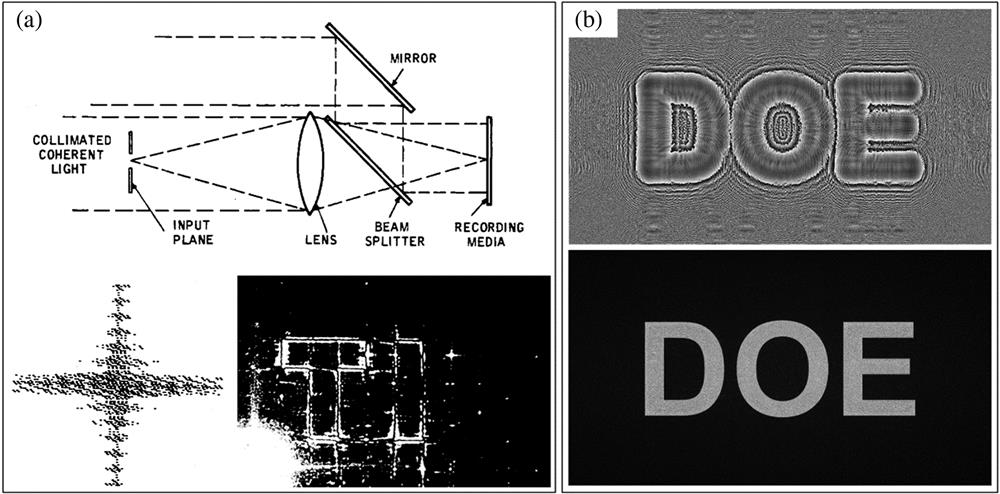
Grayscale amplitude-only holograms. Due to the inherent discrete characteristics of devices such as plotters, SLMs, and lithography systems, the representation of continuous amplitudes often necessitates discrete approximation during modulation. The most commonly employed structure for this purpose is the grayscale structure, as depicted in Fig. 1(a)[64]. In the context of grayscale amplitude-only holograms, one can envision them as two-dimensional (2D) data matrices, where each pixel is discretely represented by a specific brightness value. If each pixel within the hologram can take on discrete brightness levels, then the grayscale hologram can effectively convey bits of data.
Figure 1.Typical holograms and corresponding holographic reconstructions. (a) The grayscale amplitude-only hologram can be thought of as a 2D data matrix where each pixel is represented as a specific discrete brightness value[64]. The reconstruction of the grayscale amplitude-only hologram displays the letters “TI.” (b) The kinoform is a phase-only hologram obtained through analytic calculations. It is capable of forming a reconstructed target without any unwanted diffraction orders. In the case of the presented kinoform, its reconstruction displays the letter “DOE.”
Kinoforms. The term “kinoforms” originally referred to phase-only holograms achieved through one-step analytic calculations[65]. However, in a broader sense today, “kinoforms” can encompass any phase-only holograms, including those obtained through numerical optimization methods, as illustrated in Fig. 1(b). Kinoforms operate exclusively on the phase of an incident wave, operating under the assumption that only the phase information is necessary for reconstructing a scattering target. When compared to amplitude-only holograms, kinoforms generate reconstructed targets without unwanted diffraction orders.
Lohmann holograms. Lohmann holograms are encoded utilizing the detour phase effect[61]. In Lohmann holograms, each pixel is composed of an opaque rectangle and a transparent slit. The size of the slit governs the modulation of the amplitude, while the position of the slit determines the modulation of the phase. Consequently, Lohmann holograms fall into the category of complex holograms due to their ability to manipulate both amplitude and phase information.
2.1.3.3 Binary optical elements
The BOE has its origins in phase-only holograms, with kinoforms often regarded as the precursor to BOEs. During the early stages of computer-generated holography, obtaining CGHs was a challenging task due to the limited capabilities of plotters at that time. In this context, BOEs were developed. A BOE employs phase steps to approximate the continuous phase profile of a phase-only hologram[66,67]. It can be manufactured using methods such as etching, mold pressing, and lithography. BOEs have gained popularity due to their advantages including high diffraction efficiency, ease of fabrication, and the flexibility to design for various applications. Some typical BOEs are listed as follows.
Blazed binary gratings. A traditional blazed grating consists of periodic structures with a fixed blazed angle, designed to focus the incident beam onto a specific diffraction order. In contrast, a blazed binary grating replicates the functionality of a traditional blazed grating by adjusting the superlattice period within the periodic structure and varying the duty cycles of different phase steps within a single period[68]. Theoretical calculations indicate that the efficiency of this blazed binary grating can be as high as 88%.
Binary Talbot gratings. When a plane wave interacts with a periodic grating, it can exhibit a specific self-imaging phenomenon where the grating structures are reproduced at a particular distance. This phenomenon is known as the Talbot effect, and the specific distance at which this occurs is referred to as the Talbot distance[69]. Correspondingly, if a binary phase grating can generate a binary amplitude pattern that resembles itself, it is termed a “binary Talbot grating”[70]. Binary Talbot gratings are frequently used to transform a uniform plane wave into multiple concentrated spots with equal intensity.
Binary Dammann gratings. The Dammann grating, also referred to as a “multiple phase hologram,” essentially comprises a 2D phase distribution with distinctive groove shapes[71]. This artificial grating is used to generate a set of equally bright images arranged around the optical axis[72]. One of the advantages of Dammann gratings is their straightforward fabrication, which involves the use of a single mask. However, it is worth noting that Dammann gratings have a relatively moderate diffraction efficiency, typically around 80%.
2.2 Wavefront modulation with metasurfaces
Fermat’s principle intricately governs the reflection and refraction of light at the interface between two conventional materials. The coefficients associated with these two phenomena are derived from the Fresnel equations and Snell’s law, respectively. However, when we introduce a metasurface by replacing one of the conventional materials, a remarkable transformation occurs. This transformation arises from the alteration of boundary conditions triggered by resonant excitation. The incorporation of nanostructures results in the scattering of electromagnetic waves, imprinting complex spatial patterns of phase discontinuities. In an insightful study by Yu et al., the authors formulated generalized laws governing the phenomena of reflection and refraction in these contexts, leading to a profound understanding of this complex interplay. The key findings are outlined below[73]: where , , and represent the angles of incidence, reflection, and transmission, respectively. Meanwhile, denotes the phase gradient aligned with the plane of incidence. Additionally, an experimental demonstration of anomalous reflection and refraction within a plasmonic metasurface was illustrated, as depicted in Fig. 2(a). These generalized principles have served as a guiding framework for the advancement of innovative photonic devices. Sun et al. introduced a novel gradient metasurface, capable of converting propagating waves into surface waves with an impressive 100% coupling efficiency, under the condition that the phase gradient reaches a significant magnitude[74], as exemplified in Fig. 2(b). Furthermore, in another study, they demonstrated that a gradient metasurface can efficiently redirect incident waves into a singular anomalous reflection pathway, achieving an exceptional conversion efficiency of up to 80%, as illustrated in Fig. 2(c). Discoveries of this magnitude hold immense promise for a wide range of applications, spanning from high-efficiency surface plasmon couplers to anti-reflection coatings and light-absorbing devices.
Figure 2.Generalized reflection/refraction laws and Huygens’ metasurfaces. (a) SEM image showcases a V-shaped antenna array meticulously patterned on a silicon wafer. Within its unit cells, eight distinct V-antennas elegantly illustrate the principles of reflection and refraction. Consequently, this design forms a consistent phase gradient across the metasurface, enabling precise control over the propagation of reflected or transmitted light[73]. (b) Image of a crafted H-shaped antenna reflect-array positioned on a metallic backplane. This metasurface effectively introduces an interfacial phase gradient, skillfully compensating for the momentum mismatch between the propagating wave and surface wave. Consequently, this design enables nearly flawless conversion from plane waves to surface waves at virtually any incidence angle exceeding a critical threshold[74]. (c) Illustration of a reflect-array metasurface design, featuring gold nanorods separated from a gold backplane by a spacer. This arrangement capitalizes on the generation of robust magnetic fields when both the upper and lower gold layers are illuminated by incident light polarized along the gold rod, thanks to the near-field coupling. The efficient manipulation of radiation phase delay can be achieved by adjusting the antenna length, yielding highly effective anomalous reflection at normal incidence[75]. (d) The surface equivalence principle is utilized to create imaginary electric and magnetic surface currents, aligning with the boundary conditions. On the right side, the depiction illustrates the magnetic field (Hz) when a y-polarized wave impinges normally upon the engineered Huygens’ metasurface, with a close-up view of its individual unit cell. The Huygens metasurface exhibits the remarkable capability to redirect an incident beam with nearly perfect efficiency, achieving close to 100% refraction into a new beam[76]. (e) Illustration of a Huygens metasurface comprising an array of nanodisks, designed to generate both electric and magnetic polarization currents. This metasurface achieves full coverage of transmission phases spanning 360°, and it exhibits nearly perfect transmission, nearing unity[77].
Most of the proposed metasurfaces primarily concentrate on the manipulation of electric polarization currents. However, this limitation hampers their efficiency and their capacity to generate and precisely control desired wavefronts. In contrast, Huygens’ metasurfaces offer the unique advantage of managing both electric and magnetic polarization currents simultaneously. Huygens’ principle, a fundamental concept in wave optics, asserts that every point along a wavefront behaves as a secondary source, emitting outgoing waves. Leveraging Love’s equivalence principle[78], as outlined in Fig. 2(d), it becomes apparent that to satisfy the boundary conditions for a specific transverse field discontinuity, we must introduce fictitious electric and magnetic surface current distributions:
By implementing subwavelength texturing at the unit cell level, it becomes feasible to tailor the surface electric and magnetic polarizabilities, denoted as and , respectively. This customization allows for the achievement of the condition , where represents the impedance of the medium in the vicinity. Consequently, this precise manipulation enables the complete elimination of reflection. The complex transmission coefficient of the metasurface is mathematically represented as follows[76]:
Subsequently, the nanostructures constituting the metasurface can be meticulously designed to align the induced currents with the incident field on a single side of the metasurface. Simultaneously, on the opposite side, the inherent discontinuity is orchestrated to yield the desired wavefront transformation. In this scenario, the individual current elements effectively serve as Huygens sources, giving rise to a unidirectional response. This response not only cancels the incident field but also engenders the creation of the transmitted field, as depicted in Fig. 2(d)[76]. In a remarkable advancement, Kivshar’s research group has taken an extraordinary stride by showcasing an all-dielectric Huygens metasurface with comprehensive transmission-phase coverage spanning and achieving near-unity transmission, as illustrated in Fig. 2(e)[77]. The amalgamation of complete phase coverage and exceptional transmission efficiency positions the Huygens metasurface as a groundbreaking innovation in the realm of flat optics. It has demonstrated remarkable potential for applications such as beam shaping, precise focusing, holography, and dispersion control.
2.2.2 Pancharatnam–Berry phase and propagation phase metasurfaces
The previously mentioned metasurfaces achieve phase or amplitude modulation by altering the geometric characteristics of the meta-antennas. An alternative method for introducing sharp phase changes involves the utilization of the Pancharatnam–Berry phase (PB phase). PB phase metasurfaces can achieve comprehensive phase control by solely manipulating the spatial orientation angles of the meta-antennas while keeping the shape of meta-antennas identical. When considering an anisotropic scatter rotated by an angle , the Jones matrix is expressed as where and represent the transmission coefficients for incident light polarized along the two principal axes of the scatterer, respectively. Then for a circularly polarized light (CPL) incidence, the output light is[79]
The initial term signifies the transmission of CPL with the same handedness as the incident light, while the second term represents the transmission of CPL with opposite handedness, accompanied by an additional Pancharatnam–Berry (PB) phase. The phase modulation is twice the scatterer’s rotation angle, with opposite signs for opposite-handed CPL. Therefore, a comprehensive phase shift from 0 to can be achieved when meta-antennas rotate from 0 to .
Hasman’s group demonstrated that a metasurface consisting of coaxially rotating nanorods milled in gold film can exhibit the optical spin Hall effect (OSHE)—a lateral beam shift due to its optical spin (circular polarization helicity)[80], as shown in Fig. 3(a). The spin Hall lateral shift is induced by the PB phase arising from the spatially varying orientations of the nanorods distributed in the curved chain. Huang et al. later conducted a study showcasing a dispersionless PB metasurface, which exhibited the intriguing phenomenon of broadband anomalous refraction spanning from visible to near-infrared wavelengths[81], in Fig. 3(b). However, these PB phase metasurfaces operating at visible or near-infrared wavelengths demonstrate low polarization conversion efficiency in the transmission mode, which has limited their real applications. Zheng et al. proposed a PB phase metasurface hologram reaching diffraction efficiencies of 80% at 825 nm with a 400 nm broad bandwidth[82].
Figure 3.PB phase and propagation phase metasurfaces. (a) SEM image of a linear arrangement of nanorods with positioned angle altering along the x-axis. Incident CPL with opposite handedness will be deflected into two directions. When the structure symmetry is circular, OSHE will occur in a PB phase metasurface due to the spin–orbit interaction[80]. (b) Schematic of a refract dipole array metasurface. Normal refraction occurs when the metasurface is shed by RCP light, while anomalous refraction occurs with LCP light. On the right, SEM image of a metasurface generates an optical vortex beam in different wavelengths[81]. (c) Binocular metalens uses nanopillars with different sizes to modulate the propagation phase[85].
Propagation phase modulation is another phase modulation mechanism in dielectric metasurfaces. In contrast to the PB phase metasurfaces, propagation phase metasurfaces control the phase of linearly polarized waves passing through large arrays of nanostructures (usually nanobricks) with high aspect ratios[83,84]. The size of nanostructures plays a key role. Two orthogonal linear polarizations can be modulated independently by varying the size of these nanostructures. Recently, underwater binocular depth-sensing and imaging device [Fig. 3(c)] based on a propagation phase metalens has been demonstrated by Tsai’s group[85]. Intriguingly, using chiral meta-atoms breaks the fundamental symmetry restriction that rotation must be exerted on meta-atoms, and the PB phase and propagation phase modulations can be combined together[86].
2.3 Polarization/vector fields with micro-DOEs
2.3.1 Diffraction theory of polarization modulation in micro-scale
DOEs discussed in Section 1.1 typically feature pixel sizes significantly larger than the wavelength of the incident light. These DOEs are designed utilizing scalar diffraction models, where the impact of polarization on modulation is seldom taken into account. Consequently, these DOEs are seldom suitable for the purpose of modulating the polarization of incident light.
Nonetheless, when the pixel size of the DOE approaches the wavelength of the incident light (), a notable shift occurs in the DOE’s response to incident beams with distinct polarization states. This phenomenon can be explained physically by the variation in boundary conditions for TE and TM waves at this pixel size. Consequently, the equivalent refractive indices for the two orthogonally polarized lights differ as well. Given that the majority of energy in the diffractive distribution is concentrated on two primary orders, this type of diffraction under such pixel size conditions is often referred to as double-wave diffraction. This complex diffraction behavior can be mathematically modeled using the coupled-wave theory, based on Kogelnik models[87,88]: where represents the minimum pixel size of the DOE, stands for the diffraction angle, signifies the diffraction order, represents the wavelength in a vacuum, and signifies the equivalent refractive index. Importantly, varies with different polarization states. Consequently, this type of DOE has the capability to modulate the polarization state of incident light.
However, as the pixel size of the DOE decreases significantly, approaching , all higher-order diffractions transform into evanescent waves, leaving only the zero-order diffraction. Under these circumstances, the application of vector diffraction theory becomes imperative. Scalar diffraction theory and coupled-wave theory are no longer sufficient to accurately describe the distribution of diffractive outcomes. In vector diffraction theory, the DOE with such a minute pixel size exhibits distinct and prominent polarization features. This paradigm shift introduces a novel approach to design DOEs for polarization modulation.
2.3.2 Polarization modulation by micro-diffractive optical elements
By incorporating both coupled-wave theory and vector diffraction theory, it becomes evident that DOEs with pixel sizes approximately equal to or smaller than the wavelengths of incident light exhibit pronounced polarization characteristics. In cases where resonance in polarization modulation is not a primary concern, the mathematical representation of diffraction arising from these DOEs can be approximated using an equivalent medium theory. This theory treats small-pixel DOEs as uniform uniaxial films. Assuming the small-pixel DOE is a one-dimensional uniform grating, each grating period consists of an -part with a higher refractive index and an -part with a lower refractive index . The proportion of the -part occupying the entire grating period is denoted as . In this context, for the - and -light components, the corresponding refractive indices are expressed as follows:
Notably, small-pixel DOEs offer the advantage of adjustable refractive indices. By manipulating the design parameters of these small-pixel DOEs, it becomes straightforward to attain appropriate refractive indices tailored to different polarization states. This adaptability renders small-pixel DOEs exceptionally well-suited for polarization modulation applications.
Furthermore, incident light interacts with the guide mode of small-pixel DOEs, potentially leading to resonance effects. When the phase-matching condition is met, the incident light can also be influenced by leak-mode resonance. It is important to note that the phase-matching conditions for TM and TE waves are distinct, and the parameters responsible for inducing leak-mode resonances in these waves also differ. Consequently, when considering resonance effects in the context of polarization modulation, the design of small-pixel DOEs offers a greater degree of flexibility and additional avenues for optimization.
2.3.3 Some classic micro-DOEs for polarization modulation
Subwavelength gratings, as the term suggests, pertain to DOEs featuring pixel sizes in close proximity to or smaller than the wavelengths of incident light[89,90]. These subwavelength gratings can be broadly categorized into three types.
Subwavelength dielectric gratings. The polarization selectivity of subwavelength dielectric gratings primarily arises from the birefringence induced by structures on a uniform dielectric surface[91,92]. In most instances, these gratings predominantly produce zero-order diffraction, allowing them to be treated as dielectric films. According to the equivalent medium theory, these films exhibit varying refractive indices along the directions parallel and perpendicular to the grating, giving rise to a birefringence effect. This phenomenon is illustrated in Fig. 4(a)[93].
Figure 4.Subwavelength gratings. (a) Subwavelength dielectric grating[93]. It exhibits varying refractive indices along two orthogonal directions: one parallel to the grating and the other perpendicular to it. This disparity in refractive indices leads to the manifestation of a birefringence effect. Here, comparison of the birefringence dispersion of the subwavelength grating using the theory of electromagnetic Bloch waves (black square symbol) and finite element method (red circular symbol) is provided. (b) Subwavelength all-metal grating[95]. The TE wave undergoes reflection when interacting with the subwavelength grating. Meanwhile, the TM wave transmits through the grating, yielding its own unique electric vector distributions. These distributions provide valuable insights into the behavior of the incident waves when encountering the subwavelength grating.
Subwavelength metal gratings. Subwavelength metal gratings are constructed from lines with periods smaller than the wavelength of incident light, atop a transparent metal substrate[94]. Within the operating wavelength range, the metal grating’s substrate remains transparent. For TE waves, this grating behaves akin to a metal film, allowing electrons on its surface to oscillate freely along the grating lines when illuminated by TE waves. Conversely, for TM waves, the grating functions similarly to a dielectric film, where the small period of the grating impedes electronic oscillation under TM wave illumination. Consequently, when light illuminates the subwavelength metal grating, TE waves are reflected while TM waves pass through. This distinctive behavior generates birefringence, resulting in the polarization-selective characteristics, as depicted in Fig. 4(b)[95].
Subwavelength metal–dielectric gratings. They are achieved by juxtaposing both dielectric gratings and metal gratings on a common substrate. This configuration allows for the amalgamation of the distinctive attributes associated with both metal and dielectric gratings. Consequently, subwavelength metal–dielectric gratings harness the advantageous characteristics of both elements, resulting in a synergistic enhancement of device performance[96].
2.4 Polarization/OAM/vector fields with metasurfaces
2.4.1 Polarization multiplexing
Polarization manipulation in metasurfaces is also an important topic[97–100]. More importantly, there has been a substantial increase in interest in polarization multiplexing metasurfaces[101–105]. Typically, these metasurfaces are designed to impart unique intensities and/or phases on orthogonal linear or circular polarization, as interference effects typically occur with two polarized waves that are not orthogonal to each other. Conventionally, metasurfaces exhibiting polarization-dependent phases rely on either propagation phase or PB phase designs. Propagation phase design enables two orthogonal linear polarizations (LPs), i.e., along - and -axes, to have independent phase profiles, while PB phase design allows two circular polarizations (CPs) with opposite handedness to have opposite phase profiles[106]. However, neither of these two mechanisms alone supports elliptical polarization multiplexing. Capasso’s research group introduced an innovative method that integrates both design approaches. This mechanism enables the implementation of two arbitrary phase configurations on any mix of orthogonal states of polarization, be they linear, circular, or elliptical. Most importantly, the fabrication requirement of the metasurface is rather simple, which is using wave-plate-like-shaped nanobricks. One of the prominent applications of such design is the elliptical polarization beam splitters that deflect orthogonal polarizations at , as shown in Fig. 5(a).
Figure 5.Polarization multiplexed metasurfaces. (a) Conceptual schematic of a polarization multiplexed metasurface that combines both the propagation phase and geometric phase. Precise control of diverse orthogonal polarizations can be realized[106]. (b) Malus metasurface-based one-to-two mapping and one-to-four mapping. Every nanorod has two orientation choices. According to Malus’ law, they generate identical transmitted amplitude but distinctive geometric phase delays, which is the so-called one-to-two mapping. By adding another set of nanobrick analyzers, the one-to-four mapping is constructed. As a result, grayscale patterns on the fabricated samples display various outputs upon illumination by a series of polarization orientations of LP light and the analyzer[107].
Recently, Deng et al. proposed a so-called Malus-metasurface-assisted polarization multiplexing scheme, which allows each nano-polarizer constituting the metasurface to have two or four options to impart distinct phase profiles but keeping the same amplitude, owing to the Malus law[107]. The Malus law states that the intensity of an LP transmitted out of a polarizer follows , where is the polarization angle. This relation implies that each polarizer element has two options of orientation to produce different phase profiles with otherwise the same intensity. In a more general context, when an incident LP light with a polarization angle propagates through an anisotropic nanostructure oriented along angle , the transmitted light amplitude can be described as follows: where and represent the complex transmission coefficients along the major and minor axes of the nanostructures, respectively. In the case of an ideal polarizer where and , the transmitted intensity can be simplified as
This implies that every individual nano-antenna offers two orientation possibilities that yield the same transmitted amplitude, a phenomenon known as one-to-two mapping. If additional nano-analyzers are introduced following the nano-polarizers, the transmitted light intensity can be determined as follows: where represents the direction of the analyzer. Setting results in which apparently implies a one-to-four mapping. As a result, this design offers additional degrees of freedom for enhancing information capacity. Two varieties of Malus metasurfaces were demonstrated, capable of producing continuous grayscale patterns encoded at the sample surface. These metasurfaces also projected two-step or four-step phase-only holographic images in the far field[107], as shown in Fig. 5(b). They further realized three-channel display and encipher in multiplexing non-orthogonal polarizations based on the Malus metasurfaces[108].
2.4.2 Orbital angular momentum metasurfaces
In 1989, Coullet et al. developed the concept of optical vortex (OV), an optical analogy to the fluid vortex in hydrodynamics[109]. In 1992, Allen et al. pointed out that an OV with integer topological charge (TC) carries quantized orbital angular momentum (OAM)[110] per photon. In contrast to plane waves, OVs possess phase singularities and spiral wavefronts. Now OVs carrying OAM become an indispensable instrument for information carriers[111] and optical tweezers[112]. Generation and manipulation of OAM have attracted tremendous interest[113–115]. In conventional optics, OVs can be produced using spiral phase plates[116], forked holograms[117], and q-plates[118], which are bulky. Metasurfaces add a new dimension for OAM generation and manipulation due to their ultrathin structures[119].
In 2011, Capasso’s group not only developed the generalized laws of reflection and refraction but also demonstrated the first plasmonic OV-generating metasurface[73], as shown in Fig. 6(a). The antennas are strategically positioned to create an azimuthal phase shift ranging from 0 to , in the spirit of conventional spiral phase plates, thus producing an OV with TC under LP incidence. Subsequently, they showcased a spin–orbit conversion metasurface capable of transforming orthogonal polarizations into entirely distinct OAM states. Conventional PB metasurfaces only permit the conversion of left- and right-circular polarizations into states with opposite OAM. Here they combined both propagation phase and PB phase designs and fabricated such a hybrid metasurface, called a J-plate[120], as shown in Fig. 6(b). For instance, incidenting LCP or RCP light will generate OAM with TC and . Thus far, the rapid advancement of structured-light-based information processing technology necessitates the integration of on-chip light sources. To this end, Song’s group introduced the perovskite-based metasurface, which exploits bound states in the continuum (BICs)[121], as shown in Fig. 6(c). Ultrafast switching between LP beams and vortex beams in picoseconds has been realized, with more efficient energy depletion that is several orders of magnitude smaller than that showcased in previously reported all-optical switching. Very recently, Qiu’s research group, in collaboration with European partners, demonstrated a phyllotaxis-inspired nanosieve metasurface, drawing inspiration from natural phenomena such as phyllotaxis patterns found in pine cones and sunflowers[122], as shown in Fig. 6(d). Each meta-atom can contribute to the generation of multiple OVs both in free space and on integrated chips. This interesting and innovative nature-inspired approach may deepen our understanding of the OV generation and manipulation.
Figure 6.OAM generating metasurfaces. (a) SEM image of V-shaped antenna array patterned on a silicon wafer. The antennas are arranged to introduce phase shift emulating the conventional spiral phase plate and thereby can generate plasmonic OVs under LP incidence[73]. (b) Schematic of a J-plate metasurface. It facilitates the conversion of orthogonal polarizations into entirely independent OAM states[120]. (c) Schematic of a designed perovskite metasurface that utilizes quasi-BIC modes to realize ultrafast switching of vortex beam lasing[121]. (d) Schematic of a phyllotaxis-inspired vortex generating metasurface. Each meta-atom can contribute to multiple vortex beam generations. The emergence of diverse OAM orders is intricately linked to the arrangement of nanoholes organized into various sets of spirals. The bottom part illustrates the measured free-space profiles of Fresnel diffraction intensity when illuminated with different wavelengths[122].
2.5 Optical frequency/wavelength modulation with micro-DOEs
As discussed in Section 2.2, DOEs featuring pixel sizes significantly larger than the wavelength of incident light are often designed using scalar diffraction models. However, scalar diffraction models typically do not account for frequency modulation, rendering these DOEs unsuitable for modulating frequency.
In contrast, when dealing with DOEs having pixel sizes close to or smaller than the wavelengths of incident light, the phenomenon of resonance becomes a crucial consideration. To analyze the impact of resonance, a well-established theory known as “guided-mode resonance theory” is frequently employed. In this theory, the substrate of the DOE is conceptualized as a flat waveguide, housing a series of guided modes. When incident light interacts with the DOE, the diffracted light can propagate laterally and create resonance if its vector aligns with the wave vector of a guided mode. Simultaneously, certain modes propagate outside the flat waveguide. These modes that propagate to the outside have two significant effects: firstly, they influence the spectral characteristics of the transmitted and reflected light; secondly, different modes that couple to the outside interfere with each other. These effects give rise to the emergence of high reflectivity or transmittance within a narrow band[123]. Consequently, guided-mode resonance is a valuable tool often employed in the design of DOEs for frequency filtering applications[124,125].
In addition to utilizing small-sized DOEs, thick DOEs can also be employed to achieve narrow-band filtering. A DOE is considered a “thick element” when it meets the following condition[126]: where represents the quality factor of a DOE, stands for the thickness of the DOE, denotes the refractive index, and refers to the period of the grooves in the DOE. When , the DOE is considered thin, whereas for , the DOE is classified as thick. Thick DOEs operate within the Bragg regime, and to achieve maximum efficiency, the reconstruction wavelength of a thick DOE should be precisely adjusted to meet the optimal condition known as the Bragg condition: where is the incident angle. By carefully controlling the thickness of the DOE, it becomes feasible to achieve precise frequency filtering. This manipulation of the thickness allows for effective control over the filtering properties, making it a valuable tool in the following applications.
Subwavelength filters. They represent a distinct category of subwavelength gratings, primarily designed for frequency filtering rather than polarization modulation. However, there are instances where a single subwavelength grating can integrate both frequency filtering and polarization modulation functionalities, offering enhanced versatility and performance possibilities[127]. The example of color filtering based on a subwavelength grating showcases its potential applications[128].
Volume Bragg gratings (VBGs). The VBGs are typical thick DOEs, which can serve as effective spectrum filters due to their wavelength selectivity[129,130]. The response of a VBG-based filter is contingent on various factors, including the spatial spectrum of the gratings, the distribution of input beams, and the environmental conditions in which it is employed[130]. Recently, a phase-coded metasurface was proposed that employs the same principle but enables on-chip multiplexing in the 2D design[131].
2.6 Wavelength/frequency modulation with metasurfaces
2.6.1 Color printing
The generation of colors in resonant nanostructures, known as structural colors, is currently garnering significant and increasing interest. There are primarily two-color models: the standard Red Green Blue (sRGB) model and the Cyan Magenta Yellow Black (CMYK) model. The sRGB model, designed specifically for digital photography on computers, enables the faithful reproduction of any color situated within the sRGB triangle on the CIE 1931 color map shown in Fig. 7(a), through a non-negative additive-combination of the three primary colors red (R), green (G), and blue (B)[132]. On the other hand, the CMYK model operates as a subtractive color model, wherein cyan, magenta, and yellow are produced by subtracting red, green, and blue, respectively, from white light. Metasurfaces offer a sophisticated platform for color generation, achieved by either absorbing a portion of light while reflecting the rest or by segregating various colors through the processes of scattering, diffraction, and material dispersion. Yang’s group showcased the achievement of full-color printing at the optical diffraction limit, employing metallic nanodisks on a metallic backreflector, as shown in Fig. 7(b)[133]. The excitation of localized surface plasmon resonance (LSPR) effectively tailors the reflection spectrum of scattered light. By adjusting gaps and disk sizes, a full-color palette can be achieved in pixels smaller than half-wavelength. In addition to plasmonic metasurfaces, all-dielectric metasurfaces deliver remarkable color representations owing to their inherent low loss. Xiao and Song’s research groups harnessed the electromagnetic resonances in a titanium dioxide () metasurface to achieve full-color coverage across the entire visible spectrum, as shown in Fig. 7(c)[134]. The recent upsurge of interest in compiling various functions in one metasurface is driven by the growing demand for increased information capacity. Luo’s research group demonstrated both full-color printing and holography in a plasmonic metasurface in a size of a few centimeters, as depicted in Fig. 7(d)[135].
Figure 7.Color printing. (a) sRGB color space on CIE 1931 diagram (https://commons.wikimedia.org/wiki/File:SRGB_chromaticity_CIE1931.svg). (b) Schematic of a plasmonic color filter composed of Ag/Au nanodisks on the Au/Ag backreflector. By varying the dimensions (D) of the nanodisks and gaps (g) between nanodisks, the full palette of colors is revealed[133]. (c) Schematic and SEM image of an all-dielectric metasurface. High-reflection peaks at designed wavelengths can be generated by varying the unit sizes[134]. (d) Schematic of a silver plasmonic shallow grating (PSG)-based metasurface. Its right side shows the cross-polarized spectra of reflection by CPL at normal incidence. The demonstrated high-resonance sharpness enables highly pure color production and holograms with low crosstalk in different colors shown below[135].
Metasurface-induced spectral modulation techniques have demonstrated exceptional freedom in color design compared to natural materials. What is particularly significant is that these emerging color routing schemes enable extraordinary control over light in both the frequency and spatial domains. This capability is of paramount importance for applications in image sensor technology. Traditional color sensors employ absorptive filters, commonly known as Bayer filters, on each pixel, as illustrated in Fig. 8(a). This architecture inherently restricts the amount of detected light power per pixel, as each color pixel filter only permits approximately one-third of the illuminating light to pass through to the functional layer beneath. To overcome these substantial losses, metasurface-based color routers have been proposed as high-efficiency color splitters and filters. Light with different wavelengths is split and redirected by the nanostructure into spatially separated pixels[136], as shown in Fig. 8(a). Tsai’s group demonstrated a GaN metasurface that exhibits full-color routing at the visible frequencies[137], as shown in Fig. 8(b). However, it is worth noting that achieving color imaging with these metasurface-based color routers typically requires specific polarization incidence, such as CPL. Very recently, inverse-designed (utilizing numerical optimization methods) color routers have been introduced[138–140], as shown in Fig. 8(c). These designs exhibit significantly higher efficiency compared to conventional optical filters. Nevertheless, the 3D structures of these elements posed challenges in terms of pixel-to-pixel fabrication at visible frequencies. In 2021, Miyata et al. addressed this issue by experimentally showcasing a full-color-routing metalens made of SiN, which simultaneously acts as a color splitter and lens[136], as depicted in Fig. 8(a). Later, Zou et al. managed to greatly reduce the size of the metasurface to the pixel level, with pixel dimensions of [141], as shown in Fig. 8(d). Also in a parallel line, Xie et al. further improved the design by downsizing the pixel size to using inverse design methods[142], as shown in Fig. 8(e). These so-called single-layer pixel-level Bayer metasurfaces demonstrate significant potential to replace traditional commercial imaging sensors, particularly in devices like smartphones. These ultrathin metasurfaces exhibit an average energy utilization efficiency twice that of commercial Bayer color filters. In summary, metasurfaces hold enormous promise for applications in color image sensors.
Figure 8.Color routers. (a) Top: traditional color image sensor vs chip integrated color splitters. Bottom: SEM image of the color sorting metalens alongside the measured focal plane intensity profile of the metalens when subjected to white light illumination[136]. (b) GaN metasurface that exhibits full-color routing at the visible frequencies[137]. (c) Inverse-designed 3D color splitter specifically engineered for placement atop the image sensor pixels. Incident light is adeptly concentrated onto four pixels within a focal plane, displaying distinctive polarization-dependent characteristics[140]. (d), (e) Schematics of the pixel-level Bayer metasurfaces suitable for a CMOS imaging sensor, accommodating pixel sizes of [141] and [142], respectively.
Nonlinear optical effects play a pivotal role in frequency spectrum manipulation of laser systems[143]. Second and third harmonic generation (SHG and THG) are routinely employed in applications of frequency conversions; see Fig. 9(a). These nonlinear effects are contingent on the local electromagnetic field and are inherently of low intensity[144]. Plasmonic metasurfaces provide a compact platform for amplifying the nonlinear processes, primarily owing to the potent localized field arising from the excitation of surface plasmon polaritons (SPPs). SPPs are sensitive to the details of the geometry of nanostructures. Therefore, nonlinear effects can be achieved by engineering the geometries of metasurfaces. Konishi et al. demonstrated SHG generation and selection rules in a plasmonic metasurface with threefold rotational symmetry[145]; see Fig. 9(b). Li et al. showed the THG in a plasmonic metasurface with fourfold rotational symmetry[146]; see Fig. 9(c). Besides the plasmonic nonlinear metasurface, all-dielectric metasurfaces have become the recent research trend for investigating nonlinear optical effects. In contrast to plasmonic metasurfaces, dielectric metasurfaces can confine light inside the resonators, which greatly boosts the nonlinearities of the dielectric. Moreover, the employment of the dielectric circumvents the constraint of low-frequency conversion efficiency stemming from the intrinsic losses and low damage threshold in plasmonics[147]. Anthur et al. combined the gallium phosphide (GaP) and quasi-BIC modes in a metasurface and demonstrated the SHG with higher efficiency under otherwise lower pump intensities than previously reported dielectric metasurfaces[148]; see Fig. 9(d). The quasi-BICs mode allows very-high-quality-factor (Q) optical resonances. The THG can also be realized in the quasi-BIC metasurface[149], as shown in Fig. 9(e). Combined with suitable nonlinear dielectric materials, the proposed scheme has the potential to significantly elevate SHG and THG within metasurfaces, bringing these processes closer to the levels needed for practical applications.
Figure 9.Nonlinear metasurfaces. (a) Conceptual schematic of photon diagrams for important nonlinear processes. New frequencies (downward arrows) are generated when the material system returns to the initial states (solid lines) from the virtual quantum–mechanical states (dashed lines) driven by the input fields (upward arrows). (b) SEM image of the sample supporting SHG with threefold rotational symmetry[145]. (c) THG from a PB phase nonlinear metasurface. The metasurfaces with C2 and C4 rotational symmetries diffract RCP and LCP THG signals in different ways[146]. (d) Left: schematic of a dielectric metasurface composed of a square lattice of GaP dimers supporting quasi-BIC modes. It exhibits continuous wave SHG in the visible range. Right: SEM image of the metasurface[148]. (e) Si metasurface supporting high-Q quasi-BICs exhibiting remarkably high conversion efficiency for the THG and SHG[149].
The diffraction efficiency of DOEs can be defined as the ratio between the energy of the desired diffraction order and the energy of the incident illumination. This relationship can be expressed as follows:
A greater diffraction efficiency signifies a more luminous and well-defined reconstruction. This parameter plays a pivotal role in assessing the effectiveness of DOEs. Typically, the diffraction efficiency is intricately linked to the encoding techniques, computational models, and modulation parameters employed in the design and fabrication of these optical elements.
3.1.1 Encoding methods
As indicated in Eq. (1-4), amplitude-only DOEs are commonly encoded using off-axis interference. However, due to the presence of the DC term and other unwanted diffraction orders, amplitude-only DOEs tend to exhibit low diffraction efficiencies[64]. Enhancing the diffraction efficiencies of these amplitude-only DOEs involves replacing the constant “C” in Eq. (1-4) with an optimized distribution[150]. Nevertheless, even with this improvement, a substantial portion of energy is still wasted on undesired orders. To mitigate this issue, coaxial interference is employed for encoding amplitude-only DOEs, leading to better energy utilization when compared to off-axis interference[39]. Nonetheless, it is worth noting that even with coaxial encoding, the highest achievable energy utilization for amplitude-only DOEs remains capped at 50%.
Phase-only DOEs can be encoded through either off-axis or coaxial interference methods. In the encoding process of an amplitude-only DOE, a constant, known as the DC bias, is invariably added to the amplitude distribution to ensure that all pixels within the amplitude-only DOE exhibit positive values. However, owing to the inherent periodicity of phase, the inclusion of a DC bias becomes unnecessary when encoding a phase-only DOE. This distinctive feature simplifies the elimination of the zero-order diffraction, while other undesirable orders produced by a phase-only DOE can also be effectively suppressed through optimized distributions. In an ideal scenario, all energy can be concentrated into the desired diffraction order, enabling the theoretical diffraction efficiency of phase-only DOEs to reach 100%. In terms of efficiency, encoding a desired complex distribution into a phase-only DOE is a superior choice compared to encoding it into an amplitude-only DOE.
3.1.2 Calculation models
As outlined in Section 2.1.1, the maximum energy utilization for coaxial amplitude-only DOEs is theoretically capped at 50%. This energy efficiency is derived under ideal conditions. However, in real-world practical scenarios, achieving this ideal condition can be quite challenging, which consequently results in a further decline in the diffraction efficiency of amplitude-only DOEs. This challenge is particularly exacerbated in the case of off-axis DOEs, where the reduction in diffraction efficiency becomes even more pronounced.
Extensive research has been dedicated to investigating the diffraction efficiency of amplitude-only DOEs[151–153]. One particularly comprehensive study, conducted by Wyrowski’s group, stands out as a representative contribution[154]. In this work, a thorough analysis of the diffraction efficiency of amplitude-only DOEs was carried out, taking into account various parameters. Specifically, amplitude freedoms, phase freedoms, and scale-factor freedoms were all considered in the calculations. Among these, phase freedoms emerged as fundamentally important for enhancing efficiency. By harnessing these freedoms, it became evident that higher diffraction efficiencies could be readily achieved, as illustrated in Fig. 10. This conceptual framework of freedoms was also extended to the design of phase-only DOEs[155,156], resulting in notable advancements in diffraction efficiency for this category of optical elements as well.
Figure 10.Effect of calculation model on reconstruction quality. (a) Amplitude-only DOE is calculated by the analog method. In this approach, the DOE is generated using a random-phase-based algorithm. However, during the holographic reconstruction process, the diffraction efficiency within the target area is constrained and does not reach its maximum potential. (b) Amplitude-only DOE calculated by the freedoms-considered calculation model[154]. This model places significant emphasis on the fundamental importance of both amplitude and phase freedoms. By harnessing these different degrees of freedom in the design and optimization process, it becomes feasible to attain higher diffraction efficiencies within the target area with relative ease.
Numerous research efforts have contributed to the development of a practical framework aimed at enhancing the diffraction efficiency of DOEs[157–159]. This framework has evolved and can be summarized as follows: firstly, the application of advanced optimization algorithms, such as simulated annealing[160] and genetic strategies[161], is crucial. These algorithms take into account a broader set of design freedoms, allowing for more comprehensive optimization of DOEs. By leveraging these techniques, it is possible to achieve higher diffraction efficiencies. Secondly, it is important to account for the quantization limitations inherent in the fabrication and implementation of DOEs. To address this, a stepwise introduction of quantization constraints can be implemented. This approach helps overcome stagnation problems during the optimization process and ensures that the designed DOEs are feasible and practical for real-world applications. By incorporating these strategies, researchers and engineers can make significant strides in improving the diffraction efficiency of DOEs.
3.1.3 Modulation parameters
The diffraction efficiency of DOEs is influenced by several key parameters, including a number of phase levels, filling factor, and fabrication accuracy. Their influences are listed as follows.
3.1.3.1 Number of phase levels
In many phase-only DOEs like CGHs and BOEs, the phase profiles are not continuous. Instead, discrete phase levels are utilized to approximate a continuous phase distribution. This discretization process inevitably results in a reduction in efficiency. The diffraction efficiencies under varying numbers of phase levels can be expressed as follows[161]:
Indeed, as the number of phase levels increases, the diffraction efficiency tends to approach the efficiency of a DOE with a continuous phase profile. This convergence occurs as the discrete phase levels become finer and better approximate the desired continuous phase distribution, ultimately resulting in improved diffraction performance.
3.1.3.2 Filling factor
In certain types of DOEs, especially dynamic CGHs, continuous phase profiles are transformed into pixelated structures because of the characteristics of modulators. The conversion process can be mathematically expressed as follows[162]: where and represent the pixel dimensions, and denote the pixel pitches, stands for the discrete pixelated distribution, and represents the continuous profile. The filling factor can be defined as the ratio between pixel dimensions and pixel pitches, and it is expressed as follows:
The impact of the filling factor on diffraction efficiency can be summarized in two main aspects. Firstly, when the filling factor is reduced, there are larger gaps between pixels, which cannot effectively modulate the wavefront. This leads to a waste of light energy, as some portions of the incident light are not utilized for the desired diffraction. Secondly, the gaps around each pixel act as small rectangular apertures, contributing to the generation of unwanted diffraction orders. These additional orders disperse some of the energy away from the target orders, causing a decrease in the energy of the desired diffraction orders. Optimizing the filling factor is crucial to maximize diffraction efficiency and suppress the creation of unwanted diffraction orders in DOEs.
3.1.3.3 Fabrication accuracy
In the realm of DOEs, particularly BOEs, the fabrication accuracy plays a pivotal role in enhancing diffraction efficiency. For example, one effective strategy involves the use of multi-level structures, while achieving these structures depends significantly on the fabrication process. Here are some common fabrication methods and their associated features.
Etching Methods. In etching methods, a photoresist is coated onto a substrate (e.g., glass), and a mask is positioned on the coated substrate. After exposure to light, the exposed areas are etched away. This process yields a two-level structure. To create a multi-level DOE, this process must be repeated multiple times. Achieving high fabrication accuracy with this method can be challenging, as it requires precise control[35].
Deposition Methods. In contrast to etching, deposition methods create phase levels by depositing a film of a specific thickness onto the substrate. Deposition processes are generally easier to control, resulting in higher fabrication accuracy compared to etching methods. However, the DOEs fabricated through deposition methods may not have a high-level firmness[163].
Direct Writing Methods. Direct writing methods involve the use of a laser beam or an electron beam with adjustable intensity to directly expose the photoresist on the substrate[164]. After development, relief structures are produced. Laser beams are typically employed for structures with linewidths smaller than 0.5 µm, while electron beams are used for larger linewidths (). The fabrication accuracy of direct writing methods depends on the precise control of beam intensity.
Grayscale Mask Methods. Grayscale masks possess multi-level transmittance and are placed on the coated substrate[165]. This approach enables the direct production of multi-level structures. The accuracy of the grayscale mask method relies on the precision of the mask itself.
The schematics of the etching method, direct writing method, and grayscale mask method are shown in Fig. 11[166]. The choice of method often depends on the specific requirements of the DOE and the trade-offs between fabrication accuracy, ease of implementation, and the desired diffraction efficiency. To explain the influence of encoding methods and modulation parameters more intuitively, diffraction efficiencies of some typical DOEs are listed in Table 1.
Figure 11.Fabrication of BOEs[166]. (a) Two-step etching method. In the first step of the fabrication, a photoresist is coated on a substrate. A mask is placed on the coated substrate. After being illuminated, the exposed position is etched. By repeating this step, a complicated BOE can be fabricated. (b) Direct writing method. It employs a laser beam or an electron beam with variable intensity to directly expose the photoresist on the substrate. (c) Grayscale mask method. The grayscale mask has a multi-level transmittance. When it is placed on the coated substrate, a multi-level structure can be produced directly.
Stepping into the realm of nano-optics, fabrication accuracy is also a very important topic for metasurfaces. Conventional fabrication processes include etching methods in combination with photolithography[167–170] or electron-beam lithography (EBL)[171,172] using materials compatible with traditional CMOS processes. In addition, direct writing methods include focused ion beam milling (FIB)[173–176], laser printing[177,178], and nanoimprinting[179–187]. Especially, nanoimprint lithography (NIL) is a cost-effective and high-throughput technique for replicating nanoscale structures that do not require expensive light sources for advanced photolithography equipment. NIL overcomes the limitations of light diffraction or beam scattering in traditional photolithography and is suitable for replicating nanoscale structures with high resolution[180]. It can fabricate high conversion efficiency and high-aspect-ratio structures[179,182,183]. It has been used to fabricate the metalenses that implement augmented reality imaging[184] and holographic display[185,186].
3.2 High-efficiency metasurfaces
Ideally, the maximum working efficiency of a metasurface would be 100%, allowing it to function as either purely reflective or purely transmissive while offering full control over phase modulation from 0 to [10]. Laboratories worldwide are actively developing high-efficiency metasurfaces. For instance, in Fig. 2(b)[74], Sun et al. demonstrated a phase-gradient metasurface comprising H-shaped nanoantennas, which efficiently reflects electromagnetic waves while following the generalized Snell’s law. They extended this concept to the spectrum in near-infrared, realizing a high efficiency ()[75], as shown in Fig. 2(c). Later in 2018, Bozhevolnyi’s group showed a highly efficient multifunctional plasmonic metasurface that can deflect LP light with orthogonal polarizations and focus their reflected beams at different positions. The efficiency goes up to 65% accompanied by a polarization extinction ratio up to 30 dB[188], as shown in Fig. 12(a). Back in 2013, Pfeiffer et al. reported a Huygens metasurface that can deflect a normally incident light by an angle of 35° at the telecommunication wavelength with a high efficiency of 30%, which is an order of magnitude enhancement over previously reported metasurfaces[189], as shown in Fig. 12(b).
Figure 12.High-efficiency metasurfaces. (a) Illustration depicting a reflective gap surface-plasmon-based metasurface designed to disperse incident orthogonal linearly polarized (LP) light into distinct focal points with remarkable efficiency, reaching up to 65%, and showcasing a polarization extinction ratio of up to 30 dB[188]. (b) Schematic representation of a Huygens metasurface designed to efficiently refract light at normal incidence in the telecommunication[189]. (c) A reflective dielectric metasurface composed of high-refractive-index Si cut wires can function as a half-wave plate with perfect reflectance near unity and over 98% polarization conversion efficiency across a bandwidth of 200 nm. Combining eight sections of specially designed Si cut-wires introduces a changing phase profile azimuthally, and results in highly efficient optical vortex beam creation over a wavelength range from 1500 to 1600 nm[190]. (d) Two examples of transmissive dielectric metasurfaces with phase coverage with high-efficiency transmission up to 36% for beam deflecting (left) and 45% for vortex beam conversion (right)[191]. (e) Schematic of arbitrary complex vectorial optical fields with metasurface. The specially customized units in the metasurface can reflect a given polarization to target polarization with desired phases[193]. (f) Topology-optimized, large-area, high-numerical-aperture silicon metasurface lens designed to achieve a focusing efficiency surpassing 90%[195].
The inherent Joule heat in metals at optical frequencies restricts the application of plasmonic metasurfaces in real life. In contrast to plasmonic metasurfaces, all-dielectric metasurfaces exhibit low loss in the optical regime. Their electric and magnetic resonances are governed by Mie resonances. As mentioned earlier, Kivshar’s group demonstrated an all-dielectric Huygens metasurface with a comprehensive transmission-phase range covering 0 to and near-unity transmission[77], as shown in Fig. 2(e). The high efficiency occurs when both electric and magnetic resonances demonstrate comparable amplitudes and phases, resulting in constructive interference in the forward direction and destructive interference in the backward direction. Yang et al. demonstrated a dielectric metasurface composed of high-refractive-index silicon nano-cutwires, which can realize LP conversion with more than 98% conversion efficiency in the short-wavelength infrared regime. A similar design can also demonstrate OAM generation with high quality[190], as shown in Fig. 12(c). Shalaev et al. engineered an all-dielectric, polarization-sensitive metasurface comprising silicon nanoblocks positioned atop a bulk-fused silica substrate[191], as shown in Fig. 12(d), which showcased impressive transmission efficiencies at telecommunication wavelengths, reaching up to 45% for the vortex converter and up to 36% for the beam deflecting device, with a full phase control. Recently, as the structured light prevails in the optics research realm[192], the demand for generating complex structured light with high efficiency is urgent. In 2021, Wang et al. proposed a generic approach to generating arbitrary complex vectorial optical fields (VOFs) with a metasurface that features complete matrix distributions within an inhomogeneous Jones matrix framework[193], as shown in Fig. 12(e). They showed a custom-designed metasurface capable of producing a cylindrically polarized vortex surface plasmon wave with a high efficiency of up to 34%. This study opens the way for future structured light generation schemes. Recent studies introduced numerically optimized nanostructures for high-efficiency metasurface designs, such as inverse design[194] and topology optimization[195]. As shown in Fig. 12(f), Phan et al. proposed a so-called topology optimized metasurface that can be considered as a high-numerical-aperture (NA) metalens with focusing efficiency exceeding 90%[195]. Their novel topology optimization approach divides the desired phase profile into linear segments at the wavelength scale and employs topology optimization to individually design each section, resulting in a more computationally efficient manner compared to conventional inverse design approaches.
3.3 Broadband DOEs
In the realm of DOEs, especially BOEs, the optimization of phase level depths often caters to a specific wavelength. However, when the wavelength of incident light deviates from the designated one, the diffraction efficiency of these DOEs experiences a rapid decline. To tackle this predicament, concepts of broadband DOEs emerge. This section introduces several notable examples of broadband DOEs, which encompass harmonic DOEs, multi-layer DOEs, achromatic refractive–diffractive elements, and achromatic subwavelength DOEs.
3.3.1 Harmonic DOEs
The harmonic DOE stands out for its ability to attain high diffraction efficiencies across a range of wavelengths, all while utilizing a single type of material[196–198]. The determination of phase level depth in the harmonic DOE can be accomplished through where represents the depth of the phase level, is an integer signifying the harmonic order, denotes the designated wavelength, and corresponds to the refractive index at . It is worth noting that harmonic DOEs exhibit substantially deeper phase levels when compared to conventional DOEs. For a harmonic DOE, the diffraction efficiencies at various wavelengths can be computed through the following formula[199]: where represents the diffraction order, denotes the fraction of phase delay introduced for wavelengths other than the designed wavelength. This fraction can be expressed as follows:
From Eq. (2-6), it becomes evident that the diffraction efficiency reaches its peak when the argument of the sinc function equals zero. Consequently, for varying wavelengths, the diffraction orders corresponding to the maximum diffraction efficiencies differ.
3.3.2 Multi-layer DOEs
The multi-layer DOE excels in delivering superior performance across a range of wavelengths by leveraging multiple materials with distinct dispersion properties[200]. For instance, when employing a two-layer DOE, two additional degrees of freedom, including the depth and dispersion characteristics of the second layer, come into play. In such instances, the modulation of incident light by this DOE results in the expression of the phase change as follows[201]: where and represent the refractive indices of the two layers, and and pertain to the depths of their respective layers.
To achieve high efficiencies across , , and in the design of a multi-layer DOE, it is necessary to solve the following equations for finding the optimal layer depths: where , , , and are arbitrary integers[202]. For a visual representation of harmonic DOEs and multi-layer DOEs, please refer to the illustrations of these DOEs in Fig. 13.
Figure 13.Broadband DOEs. (a) Two-layer DOE. This DOE can excel in delivering exceptional performance across multiple wavelengths by employing two materials with distinct dispersion properties. Its utilization introduces two additional degrees of freedom, encompassing the depth and dispersion characteristics of the second layer. (b) Harmonic DOE. It can attain high diffraction efficiencies across multiple wavelengths while utilizing a single type of material. In contrast to conventional DOEs, harmonic DOEs feature significantly deeper phase levels. Moreover, it is worth noting that distinct diffraction orders yield maximum diffraction efficiencies for different wavelengths.
Owing to the presence of chromatic aberration, optical design typically avoids the use of a single lens in isolation. Instead, based on the dispersion characteristics of optical elements at specific wavelengths, two or three lenses are often employed. This approach helps to eliminate chromatic aberration by judiciously distributing the focal lengths of these lenses for specific wavelengths while allowing other degrees of freedom (such as curvature, thickness, etc.) to correct additional aberrations[203]. Achromatic refractive–diffractive elements excel in delivering exceptional performance across multiple wavelengths through the combination of refractive elements and DOEs[204–206]. Achieving achromatism is straightforward when considering the Abbe numbers of refractive elements and DOEs possess opposite signs. The Abbe numbers for refractive elements and DOEs are expressed as where , , and correspond to the wavelengths of the yellow sodium line, blue hydrogen line, and red hydrogen line (measuring 587.6 nm, 486.1 nm, and 656.3 nm, respectively). In parallel, , , and represent the refractive indices corresponding to , , and . By setting two Abbe numbers to the same value but opposite signs, chromatic aberration can be effectively eliminated, as expressed in the following equation: where and denote scale factors.
3.3.4 Achromatic subwavelength DOEs
DOEs with periodic structures smaller than the wavelength of the incident light, such as dielectric or metal subwavelength gratings, exhibit a pronounced form of birefringence. Exploiting this birefringence enables substantial suppression of color dispersion, giving rise to two noteworthy categories of birefringence-based DOEs: broadband blazed DOEs and broadband composite achromatic DOEs.
Broadband blazed DOEs. The efficiency of conventional blazed DOEs diminishes significantly when the wavelength deviates from its designed value. However, employing a DOE with subwavelength structures allows us to harness its high-dispersion property stemming from form-birefringence, thus expanding the effective bandwidth[136]. This concept has been substantiated through rigorous electromagnetic simulations.
Broadband composite achromatic DOEs. A composite achromatic wave plate comprises two or more wave plates with varying birefringent properties. By carefully matching the birefringence characteristics of these distinct wave plates, the substantial reduction of color dispersion can be achieved[207]. Nonetheless, it is worth noting that acquiring suitable birefringent materials can pose challenges. Subwavelength DOEs, characterized by strong form-birefringence, offer a similar solution to the composite achromatic wave plate. The combination of several subwavelength DOEs effectively eliminates color dispersion[208].
3.4 Broadband metasurfaces
Optical dispersion refers to the dependence of the refractive index or wave propagation speed on the frequency or wavelength of incident light. This is an intrinsic characteristic shared by both electromagnetic waves and materials. In some scenarios, strong dispersion is preferred, whereas in others eliminated dispersion is preferred. Hence, accurate control over dispersion is critical[16,209]. While in natural materials or conventional optical devices, this task is difficult, the emergence of metasurfaces offers us a flexible platform for the dispersion engineering[210–212], since the tailoring of geometric details of the nanostructures can strongly modulate their effective refractive index.
In collaboration with Zhu’s group, Tsai’s group demonstrated a GaN-based dispersion-engineered depth-sensing metalens[213]. The metalens can resolve multiple images at different depths. For example, in Fig. 14(a), the letters “A,” “B,” and “C” in different colors are imaged at different depths. Captured by a camera, the image is blurred without processing, and after image processing, each letter can be visualized clearly at various depths. Another notable example of dispersion-engineered metasurfaces is full-color routing[137], as discussed previously in Fig. 8(b). Additionally, Zhu et al. utilized the dispersion in spectroscopic applications. They proposed an aberration-corrected spectrometer[214], as shown in Fig. 14(b), where they designed and adjusted the focal spots at different wavelengths of incident light on the same flat camera plane.
Figure 14.Dispersion-engineered metasurfaces. (a) Top: illustration of a light-field depth sensing and imaging with an achromatic GaN metalens array[213]. (b) Schematic of a dispersion-engineered metalens used as an aberration-corrected spectrometer. A conventional PB phase lens focuses along a curved surface, which results in limited bandwidth and resolution while a dispersion engineered metalens focuses along a plane such that the focal spots are tightly concentrated within a specific broad bandwidth on the flat camera plane[214].
Over the past few years, a fundamental objective in metalens design is to achieve broadband achromatism, encompassing the entire visible spectrum while maintaining high efficiency. Many research groups have been devoted to accomplishing this goal[215]. For instance, Capasso’s group established criteria for achromatic metalenses, emphasizing that all transmitted wave packets should be focused simultaneously at the same spot and maintain identical temporal profiles[216], as shown in Fig. 15(a). Their metasurface comprises multiple nanofins with various dimensions but equal height, leading to a flat surface topology. They showed an achromatic focusing spanning from 470 to 670 nm, as shown in Fig. 15(a). In a parallel development, Tsai and his colleagues demonstrated an achromatic GaN metalens by introducing hollow pillars into their nanostructure library[217]. As shown in Fig. 15(b), the unit cells of the metalens consist of both solid and hollow nanopillars. By incorporating a so-called integrated-resonant unit element (IRUE) with the PB phase method, the nanopillars can be arranged and rotated carefully to precisely offer the needed phase compensations corresponding to their spatial positions. As a result, the metalens exhibits achromatic focusing ability at wavelengths ranging from 400 to 660 nm, as shown in Fig. 15(b).
Figure 15.Achromatic metasurfaces. (a) Top: achromatic focusing necessitates the synchronous arrival of transmitted wave packets from various locations at the focal point. Bottom: experimental intensity distribution of the designed achromatic metalens in the visible[216]. (b) SEM image of a GaN achromatic metalens. From 400 to 600 nm, the measured intensity distributions of the brightest spots closely align with the designed focal spots. (white lines). As a result, clear line features can be captured after color correction by the achromatic metalens[217]. (c) Schematic of a wideband achromatic metalens array designed for integral imaging. The meta-atoms are SiN nanopillars with either circular or square holes. The measured field intensity patterns between 430 and 780 nm show perfect achromatic focusing ability in the visible wavelength[218]. (d) SEM image of a achromatic metalens. Four types of nanostructures are employed as the building blocks: circular, ring, square, and bipolar concentric ring-shaped nanopillars with high aspect ratios of around 37.5[219].
These pioneering works have paved the way for achromatic imaging operating in the entire visible region, and since then, numerous follow-up works have further advanced the field. In 2019, Fan et al. demonstrated an integrated imaging 3D display system based on a wide-band achromatic metasurface lens array[218], as shown in Fig. 15(c). The system employs a broadband achromatic metasurface lens array that operates across the entire visible region, machined using silicon nitride. By producing a metasurface array, a color achromatic integrated imaging 3D display system was successfully built. This work is expected to be applied in fields such as true 3D near-eye display, augmented reality, virtual reality, image encryption, security, and even 3D printing lithography. More recently, Xiao’s group demonstrated both the development of versatile fabrication skills of record-high-aspect-ratio nanopillars and a high-efficiency (average efficiency up to 88.5%) achromatic metalens working at the wavelength range of 650–1000 nm[219], as shown in Fig. 15(d).
3.5 Wide-angle/high-numerical-aperture DOEs
3.5.1 Diffraction angle enlargement by plane wave
When an illumination wave encounters a DOE, it undergoes a change in its propagation direction. Assuming the incoming illumination to be a plane wave, the alteration in its propagation direction after interacting with the DOE can be defined as where and denote the refractive indices of the materials before and after interacting with the surface of the DOE, and represent the incident angle and the diffraction angle, signifies the diffraction order, stands for the wavelength of the incident illumination, and corresponds to the period of the DOE. In the case of a DOE illuminated under normal incidence, the expression for the first-order diffraction can be simplified as follows:
In this equation, when both and are equivalent to , larger diffraction angles are associated with smaller periodic sizes[220,221]. In the manufacturing process of DOEs, particularly those reliant on lithography-based methods, it is generally more challenging to produce wide-angle elements compared to their small-angle counterparts. Achieving a reduced periodic size demands the use of sophisticated equipment, meticulous control, and advanced materials, all of which contribute to a substantial increase in production costs.
To enhance the diffraction angle capabilities of DOEs, numerous solutions have been proposed. One such example is the approach introduced by Kong’s group, which enlarges the diffraction angle of the Fresnel field through the introduction of an intermediate plane and the utilization of a two-step diffraction calculation[222]. By applying zero-padding to the DOE plane, the sampling interval on the intermediate plane is reduced, resulting in an effective extension of the size of the Fresnel diffraction field when illuminated with a plane wave, as visually depicted in Fig. 16. In this figure, the parameter represents the coefficient relating to the size relationship between the magnified and original DOE planes.
Figure 16.Wide-angle micro-DOEs. (a) Through the application of zero-padding to the DOE plane, the sampling interval on the intermediate plane was reduced, consequently leading to a notable extension in the size of the Fresnel diffraction field when illuminated with a plane wave. (b) Experimental results when (top) and (bottom). The sizes of corresponding Fresnel diffraction fields are and , respectively[222].
3.5.2 Diffraction angle enlargement by spherical wave
Besides using plane waves, spherical waves are often employed to broaden the diffraction angle capabilities of DOEs. Qu’s group introduced a Fresnel diffraction algorithm based on divergent spherical waves, incorporating a double-sampling strategy to physically expand the projection angle of the reconstruction[223]. Chang’s group, on the other hand, presented an algorithm based on convergent spherical waves, utilizing the off-axis double-phase strategy to overcome limitations in diffraction angles imposed by the large pixel size of the SLM, as discussed in Ref. [224]. Pang’s group extended the diffraction angle even further using a three-step diffraction calculation approach based on divergent spherical waves[225]. In this method, the sampling interval on the image plane was correlated with the position of the virtual plane, providing flexibility to achieve larger reconstructions.
The spot size created by focused light is determined through the Abbe formula . The quantity denotes the numerical aperture (NA), which describes the ability of a lens to focus light. Most metasurfaces have been designed to work near normal incidence, which hinders their practical application. Different approaches have been explored to develop metasurfaces with high-NA[171,226–229]. For instance, Liu et al. demonstrated a wide-angle Fourier metalens working well for 0°–60° of incidence angle. The design principle is as follows: for each incident angle , there is a corresponding focal offset distance denoted as from the origin[230], as shown in Fig. 17(a). An additional phase is required to compensate for the phase accumulation along propagation to get the desired focusing functionality, and this is expressed as where , represents the wavevector of the incident wave while stands for the focal length, and denotes the coordinate along the lens’s surface. By applying a first-order Taylor series approximation, the equation above can be simplified as
Figure 17.Wide-angle high-NA metasurfaces. (a) Design and fabrication of a high-NA Fourier metalens[230]. (b) Design of a high-NA divergent metalens[171].
Substituting for a Fourier lens, they obtain , which is negligible but not free. Together with a compensation of the initial phase realized by their design of high-aspect-ratio silicon waveguides, high NA can be achieved. In another example, Arbabi et al. reported a highly efficient high-NA metalens based on high-contrast transmitarrays (HCTAs)[226]. The metalens is composed of periodic silicon posts with identical lattice spacing but varying sizes, which function as different scatterers that can provide phase response covering the entire 0 to range. The metalens exhibits high focusing efficiency of up to 82% and FWHM spot size down to . In parallel, Dong’s group demonstrated a micro-sized divergent metalens with near-unity NA and subwavelength resolution, and a centimeter-sized SiN divergent metalens exhibiting high-quality wide-angle imaging[171], as shown in Fig. 17(b). With CMOS compatibility of SiN materials, this work may inspire future work to integrate metalenses into optical fibers, smart phones, and telescopes.
3.7 Dynamic DOEs
Dynamic modulation is achieved through the use of dynamic micro-DOEs. These dynamic micro-DOEs are typically categorized into three distinct types based on their modulation features: switchable, tunable, and reconfigurable.
3.7.1 Switchable and tunable micro-DOEs
Switchable micro-DOEs exhibit only a limited number of fixed states. These states change correspondingly when external conditions, typically voltage, are altered[231]. As the state changes, the switchable element displays varying diffractive characteristics. An illustrative example of a switchable micro-DOE is depicted in Fig. 18(a)[232]. This particular switchable element is constructed using helix ferroelectric liquid crystals. In the absence of voltage, the element remains in a non-diffractive state. However, upon the application of a 5 V voltage, the element undergoes a transition from a non-diffractive to a diffractive state. Thanks to the fast-response properties of the material, this element achieves remarkably rapid switching speeds, typically on the order of .
Figure 18.Switchable and tunable micro-DOEs. (a) Switchable micro-DOE[232]. This element operates with two distinct fixed states. In its default state, when no voltage is applied, the element remains in a non-diffractive state. However, upon the application of a 5 V voltage, the element switches to a diffractive state. In the non-diffractive state, the resulting reconstruction consists of a single spot. Upon transitioning to the diffractive state, the reconstruction transforms into a series of spots. (b) Tunable micro-DOE[235]. This combined DOE comprises two separate DOEs. The adjustment of the focal point positions for the combined DOE is achieved by rotating the second DOE.
In the case of a tunable micro-DOE, optical functionalities such as lens focus, prism deflection angle, and grating period can be adjusted as needed[233,234]. An illustrative example of a combined tunable DOE is presented in Fig. 18(b)[235]. This combined DOE comprises two distinct DOEs. By rotating the second DOE, the focal points of the combined DOE can be precisely tuned.
While switchable and tunable micro-DOEs offer limited degrees of freedom in dynamic modulation, they bring forth intriguing properties such as reduced pixel sizes and faster switching speeds. These DOEs find particular suitability in applications where the full flexibility of reconfigurable DOEs is not a requirement.
3.7.2 Reconfigurable micro-DOEs
In contrast to switchable and tunable micro-DOEs, reconfigurable micro-DOEs offer greater flexibility. They can undergo more arbitrary changes in optical functionality, such as transitioning from a lens to a grating, enabling wavefront modulation with a higher degree of freedom. Based on their operational features, reconfigurable micro-DOEs can be categorized into two main groups: microelectromechanical-system (MEMS) DOEs and liquid crystal (LC) DOEs.
3.7.2.1 MEMS DOEs
MEMS devices are constructed from miniaturized mechanical and electro-mechanical elements, typically manufactured using microfabrication techniques. These devices can be classified into a wide range of subdivisions. In terms of mechanical structure, some MEMS devices boast simplicity, featuring no moving parts, while others showcase intricate designs with numerous moving components. Moreover, when considering physical dimensions, MEMS devices can vary significantly. Some possess minute minimum units with physical dimensions smaller than 1 µm, while others exceed 1 mm in size. In this section, we introduce two prominent examples of MEMS DOEs: the digital micro-mirror device (DMD) and the deformable mirror (DM).
DMD. The DMD is a type of MEMS-based DOE consisting of a series of periodically arranged micro-mirrors[236], as depicted in Fig. 19(a)[237]. Each micro-mirror within the DMD can be individually addressed and controlled, offering three distinct states: on, representing a micro-mirror rotation by a certain angle (typically ), off, signifying a contrary rotation angle (usually ), and float, denoting a state with no rotation. By manipulating the state of each micro-mirror, various patterns can be generated. Given the small size of these micro-mirrors, ranging from several microns to tens of microns, they produce strong diffractions across commonly used wavebands. Consequently, different patterns on the DMD yield distinct diffractive reconstructions. The DMD boasts a high pixel count, often reaching hundreds of thousands, enabling precise modulation of the incident wavefront.
Figure 19.Reconfigurable micro-DOEs. (a) DMD[237]. It is a type of MEMS DOE that consists of a series of periodically arranged micro-mirrors. These micro-mirrors can be addressed and controlled separately. For each micro-mirror, it has three states: on, off, and float. By controlling the state of each micro-mirror, different patterns can be obtained. (b) DM[238]. It is a MEMS-based modulation device whose shape of the surface can be changed. By controlling the shape of the surface, different patterns can be obtained. (c) LCoS device[239]. It has a similar design concept to DMD. Both of them are reflective elements. The state of each pixel in the LCoS device can be changed by addressing and controlling signals. The major difference between LCoS and DMD is that LCoS modulates the phase of the incident light, while DMD modulates its amplitude.
DM. Unlike the DMD, the DM is a MEMS-based modulation device capable of altering the shape of its surface, as illustrated in Fig. 19(b)[238]. By actively controlling the shape of its surface, various patterns can be generated. When incident light is reflected by the pattern on the DM, both the amplitude and phase of the incident wavefront undergo changes, resulting in different reconstructions. Notably, the precision of wavefront modulation with a DM relies on the level of precision achieved in altering the surface shape. This precision is contingent on the number of actuators employed, which can range from several dozen to several thousand, with higher actuator counts equating to more accurate wavefront modulation.
3.7.2.2 LC DOEs
LC DOEs, also commonly referred to as LC SLMs, represent another category of reconfigurable elements[240,241]. These devices specialize in modulating the phase of incident light, yielding desired diffractive reconstructions at specific distances. LC SLMs often feature pixelized structures, where each pixel can be independently addressed and controlled. Typically, the state of each pixel is manipulated through electronic controlled birefringence (ECB). To maximize the diffraction effect, it is advantageous for the pixel size of LC SLMs to closely match the wavelength of the incident illumination. LCoS is a prominent example, with pixel sizes comparable to the illumination wavelength. This technology is widely employed for dynamic diffractive modulation.
LCoS devices and DMDs share a similar design concept. Both of them are reflective elements. Additionally, the state of each pixel within an LCoS device or DMD can be altered through addressing and control signals[242]. However, the key distinction between LCoS and DMD lies in their mode of modulation. An LCoS device modulates the phase of incident light, whereas DMD modulates its amplitude. The typical structure of an LCoS device, as depicted in Fig. 21(c)[239], involves a reflective mirror positioned on a silicon substrate, with an LC layer coated onto the reflective mirror’s surface. When pixels on the LC layer are in an open state, incident light is reflected by the pixel mirror. Conversely, when pixels on the LC layer are closed, incident light is blocked. This unique mechanism allows LCoS devices to effectively modulate incident light, generating desired diffractive reconstructions on the target plane.
3.8 Dynamic metasurfaces
Static metasurfaces are limited in their applications because they exhibit unchanged functions after fabrication. The recent surge of interest in tunable metasurfaces is driven by advancements in nanofabrication techniques and an increasing sophistication in employing various types of materials. Typically, dynamic modulation of light in tunable metasurfaces is realized based on two main mechanisms: using materials with tunable properties and incorporating mechanically movable components.
3.8.1 Liquid-crystal-integrated metasurfaces
Liquid crystals (LCs) exhibit very strong and broadband optical anisotropy and can be efficiently controlled by external factors like temperature changes[243] and electric field[244]. LCs offer substantial refractive index changes, making them a highly attractive choice for hybrid metasurface designs. Metasurfaces are particularly sensitive to refractive index changes on their surfaces, making LCs one of the most popular materials for integration in such designs.
Buchenev et al. introduced an electrically actuated switching mechanism for LC directors[245], as shown in Fig. 20(a). The LCs were integrated with a suspended metasurface with zigzag nanobridges. By switching on and off the bias between neighboring nanobridges, the orientations of the LCs can be changed. Such a two-way active switching not only modulates the refractive index of LCs but also controls the spatial distributions of nanostructures. Therefore, the resonant response of the proposed LC-integrated metasurface showed its flexibility in controlling the magnitude and wavelength with spectral tunability approaching the theoretical limit of 9%. Li et al. proposed an electrically actuated digital metasurface device (DMSD) for light-projection displays[246] in Fig. 20(b). The DMSD has unit pixels composed of Au nanorods, LCs, and extra electrode layers in each unit cell. The alternating columns of the Au nanorod are coated with either high birefringence LCs () or PMMA (), where is a constant and can be dynamically changed by switching the external bias on and off. By putting multiple such independent pixels onto one device, the DMSDs exhibit outstanding performance characterized by high-intensity contrast, rapid switching within the millisecond time range, and exceptional reversibility. Hu et al. harnessed the polarization tunability to showcase in a metasurface an electrically tunable multifunctional polarization-dependent metasurface (ETPM) integrated with LCs operating in the visible range[247], as shown in Fig. 20(c). The metasurface is built on PB-phase-based nanorods. By applying various voltages to the electrodes above the LC cell and beneath the metasurface, the orientation of LCs is modulated to attain a variable wave plate with varying phase retardations. Using this design, they experimentally demonstrated a varifocal metalens and switchable multicolor hologram.
Figure 20.Liquid-crystal-integrated metasurfaces. (a) Diagram illustrating the off and on states of a metasurface integrated with liquid crystal, which can be controlled in-plane electrically through voltage bias. The metasurface is composed of zig-zag suspended Au-SiN nanobridges as shown in the SEM image. A 110 nm ()-spectral tuning was observed for applied voltage ranging from 1.5 to 2.7 V[245]. (b) Top: digital metasurface device (DMSD) designed for use in light projection displays. The metasurface is composed of an array of pixels, with each pixel containing gold nanorods arranged in a rectangular lattice. Bottom: working principle of the DMSD. Each array is encapsulated in a liquid crystal cell that is independently tailored via an addressable electrode. Hence, reflection from pixels can be programmably controlled, and the desired images can be displayed in the far field[246]. (c) Top: illustration depicting an ETPM integrated with liquid crystals and employing all-dielectric metasurfaces. Bottom: by applying electrical modulation of different voltages, various phase abruptions can be achieved by manipulating the orientations of liquid crystal molecules, and thereby a varifocal metalens for different wavelengths is realized[247].
Modifying the materials’ optical properties through changes in their morphology is another approach that has been recently explored in dynamic metasurface designs. (germanium–antimony–tellurium, GST) is one of the first and popular material candidates that is widely used in hybrid metasurface designs due to its good thermal stability during temperature-induced dielectric–metal phase transitions. When subjected to annealing within the temperature range between the glass transition and the melting point, GST undergoes a transformation from an amorphous state into a metastable cubic crystalline state, resulting in a significant contrast in dielectric properties between the two phases[248,249]. In 2010, the first phase change metasurface composed of gold split-ring-resonator film covered by gallium lanthanum sulfide (GLS) was reported by Zheludev’s group, and the spectral resonance exhibits a dramatic blueshift of 150 nm as the GLS’s phase changes from the amorphous to the crystalline state[250]. Later, to improve this design the GLS layer was replaced with GST[251]. In 2015, Zheludev’s group proposed a GST-based metasurface that is rewritable and reversible, allowing for flexible alternation of the optical properties of the GST[252], as shown in Fig. 21(a). As an example, such a metasurface can be used as a write–erase–write double-Fresnel zone-plate that sustains multiple reconfiguration cycles. The phase change Fresnel zone can split a plane wave into two parts and focus them differently, and these Fresnel zone patterns can be independently erased and restored so that the focal spots can be dynamically controlled. Most recently, two independent works have expanded the tunability of phase change metasurfaces’ beyond optical writing and thermal annealing[253]. Brongersma’s group demonstrated a tunable GST-based optical metasurface composed of nanostrips made with both silver and GST, which modulates the scattering up to an efficiency of 30% or so. They also demonstrated a GST-Ag metasurface that can be electrically modulated in its reflectance exceeding fourfold[254], as shown in Fig. 21(b). Meanwhile, Hu’s group presented a GSST()-based metasurface that exhibits a reflectance modulation also of [255], as shown in Fig. 21(c). Unlike GST, GSST, working in the near-infrared, is a novel phase change material that exhibits broad transparency. These achievements show promise for a wide range of applications, including dynamic holography, beam deflection, DOEs, adaptive optics, and sensing.
Figure 21.GST/VO2 metasurfaces. (a) Left: schematic of the writing of dynamic phase change metasurfaces and devices. Here, (GST) is employed as the phase change material. Optical excitation by femtosecond pulses through the “write” channel alters the dielectric constant of the GST by transition between the amorphous–crystalline states. Using different illumination conditions, the working pattern can be cleaned through “read” channel[252]. (b) Schematic of an electrically actuated GST-Ag metasurface. Set and reset pulses generate heat within the metasurface, leading to a reversible transformation between its amorphous and crystalline states. The on/off ratio of the reflectance modulation can be up to 4.5 at the wavelength of 755 nm[254]. (c) Schematic of a (GSST) metasurface demonstrating reflectance modulation of [255]. (d) Gold split ring resonator–vanadium dioxide () metasurface. The resonance frequency decreases when the “insulator” becomes a “metal”[257]. (e) Thermally controlled resonance of the antennas[258]. (f) Mie-resonant dielectric metasurface based on material. Tunable extinction with temperature variation can be realized[259].
Another phase change material that has been recently used is vanadium dioxide (). Its dynamic phase change relies on the crystalline-to-crystalline transition and, as a result, does not induce the creation of surface roughness typically observed during an amorphous-to-crystalline transition[256]. The phase transition of is most frequently triggered thermally. In 2010, Basov’s group reported a -integrated gold split-ring-resonator metasurface that shows electrically controlled persistent frequency tuning and allows the enduring alteration of its response to be achieved through the use of a transient stimulus[257], as shown in Fig. 21(d). Muskens et al. in 2016 achieved this transition in picoseconds. They showcased a plasmonic metasurface, where observation of temperature-modulated spectral response in the vicinity of the phase transition is realized[258], as shown in Fig. 21(e). They further performed a fast picosecond optical pumping and probing experiment on the metasurface, which shows rapid switching at a rate on the order of six. These properties make -based metasurfaces highly attractive for use in ultrafast photonic devices. Recently, Tripathi et al. demonstrated a silicon Mie metasurface based on an insulator-to-metal phase transition mechanism in at telecommunication wavelengths[259], as shown in Fig. 21(f). Such design enables the metasurface to exhibit tunable extinction properties with variations in temperature, making it possible to customize it to create a perfect adjustable absorber.
3.8.3 Chemical reaction metasurfaces
The metal–insulator transitions during chemical reactions are another mechanism exploited in active metasurfaces. Liu’s group pioneered this research field. In 2017, they proposed a catalytic magnesium (Mg) metasurface that exhibits a dynamic plasmonic color display[260]. As shown in Fig. 22(a), the metasurface is composed of multiple pixels distributed in a squared lattice, and each pixel consists of hydrogen()-responsive Mg nanoparticles adsorbed within Ti/Pd capping layers by a layer of Ti. Upon exposure, the plasmonic colors are erased due to the phase change from Mg to . After exposure, colors are restored via the transformation of back to Mg. This mechanism is applied to information display and erasion, as can be seen in Fig. 22(a). Utilizing this mechanism, they later demonstrated printing dynamic colors in pixelated Fabry–Pérot cavities by grayscale nanolithography[261], a dynamic metasurface hologram for advanced optical information processing and encryption[262], and a dynamic dual-function metasurface device operating in the visible frequency range, capable of switching dynamically between holography and color display.
Figure 22.Chemical reaction metasurfaces. (a) Top: working principle of a hydrogen-responsive plasmonic metasurface. The colors in the metasurface can be eliminated under exposure of , and restored in . Bottom: evolution of color erasing and restoring for an optical image during hydrogenation and dehydrogenation[260]. (b) Top: schematic of an electrochemically controlled plasmonic metasurface based on voltage-responsive PANI. Bottom: integrating two addressable metasurfaces enables the electrochemically switchable holography display[263].
While chemical-reactive metasurfaces have the capability to produce colors with high purity, it is important to note that the chemistry tuning process is generally a slow procedure, in which a full erasing–restoring cycle takes thousands of seconds, as can be seen in Fig. 22(a). In 2021, to improve this innovative scheme, the Mg was replaced with a novel material, polyaniline (PANI)[263]. As shown in Fig. 22(b), PANI can be electrochemically switched between emeraldine state (ES, oxidized form) and leucoemeraldine state (LS, reduced form), and in this process its refractive index experiences a dramatic change. Most importantly, ultrafast switching of PANI is achieved electrochemically, i.e., in 1 µs. They fabricated two sets of gold nanorods organized in alternating rows on a quartz substrate coated with ITO. They are selectively covered either by PMMA or PANI. The metasurface showed remarkable contrast of intensity up to 860:1, rapid switching rate around 35 ms, and excellent reconfigurability.
3.8.4 Mechanically reconfigurable metasurfaces
Intuitively, it is understood that altering the spatial distribution of nanostructures will lead to a dramatic change in responses to light. Efforts have been dedicated to achieving this goal in metasurfaces. For instance, metasurfaces placed on a stretchable substrate such as polydimethylsiloxane have been reported[264,265]. Additionally, a pneumatic-actuated handedness-switchable chiral metasurface[266] and pneumatic-actuated nano-kirigami metasurfaces with substantial reflection modulation[267] have been demonstrated by manipulating the air pressure difference above and beneath the metasurface.
Exceptional opportunities for novel spatially reconfigurable metasurfaces are provided by electromagnetic forces at the nanoscale[268]. By introducing the maturely developed microelectromechanical system (MEMS) and nanoelectromechanical system (NEMS) into the metamaterial world[269,270], we have witnessed a rapid development of reconfigurable photonic metasurfaces. The actuation mechanisms of reconfigurable nanomechanical photonic metasurfaces mainly fall into four parts[268]: thermal, magnetic, electrostatic, and optical actuations.
Zheludev’s group demonstrated a thermally actuated metasurface. The different responses to temperature changes in membranes made of gold and silicon nitride (SiN) make the metasurface bendable. This stems from the differential thermal expansion coefficients between these two materials[271], as shown in Fig. 23(a). The metasurface is composed of alternating reconfigurable/non-reconfigurable nanobridges cut from a membrane. The reconfigurable nanobridges consist of Au-SiN layers, whereas the non-reconfigurable nanobridges consist of Au-SiN-Au layers. On change of the ambient temperature, reconfigurable nanobridges exhibit temperature-activated deformation while the non-reconfigurable nanobridges do not. Such relative displacement between neighboring bridges induces a modification in the electromagnetic coupling between adjacent meta-atoms, leading to a relative transmission change of up to . Similar to the goal of creating relative displacement between adjacent plasmonic resonators, Valente et al. reported a magneto-optical metasurface modulated by the Lorentz force induced by currents and magnetic field[272], as shown in Fig. 23(b). Also, an electro-optical version was demonstrated by Ou et al.[174], where up to 8% reversible changes of transmission and reflection in the near-infrared were observed under a bias of no more than 2.4 V. Another in-plane electrostatic actuation metasurface is demonstrated by Karvounis et al. with a rather simple nanostripe[173], as shown in Fig. 23(c), which exhibited a giant electro-optical effect. Later, Zhang et al. presented an out-of-plane electrostatic actuation mechanism[176], as shown in Fig. 23(d). In this configuration, giant electrogyration that is six orders of magnitude stronger than any natural medium emerges as electrostatic forces acting against forces of elasticity change the chiral configuration of the metasurface’s nanoscale building blocks and consequently its polarization rotatory power. Using optical forces, a pump laser beam can induce reversible displacements of the nanostrings with different nanostructures placed on them, and result in the modulation of a probe beam[273], as shown in Fig. 23(e). Recently, a piezoelectricity rotated varifocal 6G metasurface has been demonstrated[274], as shown in Fig. 23(f). Ultrafast dynamic control of the focal spots in 3D space is enabled by rotating the metasurface with assistance of the piezoelectric ceramic technology. These recent proof-of-principle examples of reconfigurable nanomechanical photonic metasurfaces signify the emergence of a new direction for advancing dynamic light modulation schemes.
Figure 23.Nanomechanical metasurfaces. (a) Thermally tunable metasurface consisting of reconfigurable and nonreconfigurable nanobridges, where the reconfigurable part is steered by a differential thermal response in Au and SiN. A relative transmission change of up to was demonstrated[271]. (b) Schematic of current carrying zig-zag-shaped nanostrips that are driven by the Lorentz force. A large reciprocal magneto–electro–optical effect was observed[272]. (c) All-dielectric reconfigurable metasurface electro-optic modulator. It can modulate the transmission spectra, which results in a giant electrostriction[173]. (d) Electromechanically reconfigurable chiral metasurface. It comprises alternating conductive and isolated nanobeams that are all perforated with alternating large and small semicircular notches. Such design was chosen to form a simplified (2D) spiral-like hole, which can be deformed into a 3D helix-like geometry by their mutual out-of-plane displacement actuated by the electrostatic force between the metasurface and another ITO-coated back-plane. As a result, giant eletrogyration that is six orders of magnitude stronger than that in natural materials such as quartz was observed[176]. (e) Light-induced giant optical nonlinearity in a plasmonic reconfigurable metasurface. Differential optical forces by a pump-laser illumination exerted on metasurface arrays cause nanoscale reversible mutual displacements of neighboring narrow and wide nanowires. This process can significantly modulate the transmission of another probe beam. The modulation strongly relies on the intensity of the pump beam[273]. (f) 6G meta-device driven by piezoelectricity realizing 3D varifocal. The 3D printing method is used for the THz meta-device fabrication. Metasurfaces are rotated accurately in real time to realize ultrafast dynamic control of the focal spots[274].
2D materials provide an exciting and newer material platform for the development of ultracompact and ultrathin devices due to their atomic thickness and exotic optoelectronic properties. Their plasmonic properties determined by the carrier density can be tuned electrically, chemically, or optically[275], which renders them great potential in tunable nanophotonics. More remarkably, integrating 2D materials with metasurfaces enables an advanced light–matter interaction manipulation and can fully exploit the potential of 2D materials. Here we highlight some most recent advancements of hybridizations of metasurfaces with 2D materials.
Li et al. presented a grating-loaded hexagonal boron nitride (hBN) metasurface that supports phonon polaritons with hyperbolic dispersion[276], as exemplified in Fig. 24(a). The hBN thin layers were laterally structured into a grating consisting of nanoribbons separated by air gaps, to form an in-plane hyperbolic metasurface (HMS). HMSs are uniaxial metasurfaces with two in-plane permittivities having opposite signs[277]. The proposed design represents a suitable basis for mid-infrared HMSs. Hu et al. presented a PB phase Au metasurface covered by tungsten disulfide () that directs the SHG photons with opposite valleys into opposite directions[278], as shown in Fig. 24(b). is a 2D transitional metal dichalcogenide (TMDC) that exhibits great nonlinearity at the valleys. Upon LP illumination, the metasurface has strong SHG from the valley band of . Most importantly, opposite spin components of the valley photons will be separated along differential directions. Meanwhile, Sun et al. demonstrated a metasurface carved with asymmetric grooves supporting unidirectionally propagated SPPs under CPL illumination. When the metasurface is covered by another TMDC, monolayer , excitons resulting from different valleys will couple intensively to the SPPs, propagating along opposite directions[279], as illustrated in Fig. 24(c).
Figure 24.Metasurfaces integrated with 2D materials. (a) hBN hyperbolic metasurface supporting strongly volume-confined phonon polaritons[276]. (b) metasurface with tunable nonlinear valley-locked chiral emissions[278]. (c) Metasurface consisting of a monolayer on subwavelength asymmetric gratings that can spatially separate opposite valley excitons[279]. (d) Patterned WS2 zone plate supporting excitons that enhance and modulate the focusing efficiency by 33% by the electrical gating[280]. (e) Twisted bilayer structure that can realize topological transitions in dispersion engineering when the relative orientation between the layers is rotated to a magic angle[281]. (f) Tunable unidirectional nonlinear emission from a truncated cone metasurface[283].
The examples mentioned above demonstrate the advantage of boosting the generally weak optical responses in thin-film 2D materials utilizing metasurfaces. Figure 24(d) shows a tunable metalens made of a patterned WS2 zone plate fabricated by van de Groep et al[280]. The monolayer was directly carved into concentric rings on a sapphire substrate. The exciton resonances of the can be altered via electrical gating. As a result, they showed that electrical gating has the capability to fully activate or deactivate the exciton resonance, thereby enabling a 33% modulation in the focusing efficiency of the metalens. Recently, Hu et al. demonstrated how rotation plays an important role in the topological transitions from hyperbolic to elliptic for phonon polaritons in twisted -phase molybdenum trioxide () bilayers[281], as shown in Fig. 24(e). As the rotation angle reaches the magic angle, the bilayer isofrequency contour will be flattened, exhibiting low-loss polariton canalization tunability and highly collimated diffractionless propagation. This study utilized the moiré hyperbolic metasurface concept and provided an avenue for twist-angle-controlled dispersion engineering. Later after the introduction of the magic-angle concept to the optics community, Mao et al. developed a magic-angle laser using photonic moiré graphene lattices[282]. Figure 24(f) presents an example of a metasurface-based nonlinear light-source composed of high-refractive-index single-crystal truncated nanocones[283]. Nauman et al. demonstrated that in contrast to the behavior exhibited by typical nonlinear metasurfaces that emit different channels of harmonic beams, the use of enables only zero-order emission of the SHG or THG signals. More remarkably, the SHG emission direction can be tuned back and forth by controlling the incident wave’s wavelength, polarization, and the metasurface itself. Therefore, the examples discussed above showcase the encouraging potential of 2D materials in nanophotonics, and more paradigm-shift developments of metasurfaces hybridized with 2D materials should be explored in the future.
4 Applications of Light Field Manipulation
4.1 Information acquisition
Micro-DOEs offer a host of advanced features, including high diffraction efficiency, distinctive dispersion characteristics, unique optical properties, and expanded degrees of design freedom. These attributes render them well-suited for capturing light field information. In this section, we will delve into two notable applications of DOEs in the realm of imaging: diffractive imaging lenses and coded apertures.
4.1.1 Diffractive imaging lenses
Diffractive lenses offer the same functionality as traditional lenses but with the advantage of a smaller volume and reduced weight, making them valuable components for imaging purposes[284]. An experiment by Meem showcased the practical use of two concatenated millimeter-scale flat lenses, achieving variable focal length and magnification for full-color video imaging, as depicted in Fig. 25(a)[285]. The numerical aperture and size of these flat lenses can be conveniently enhanced by refining the fabrication process. In comparison to metalenses and even conventional refractive lenses, these diffractive lenses are simpler to manufacture. Consequently, they find applications in lightweight, high-quality video imaging across various domains.
Figure 25.Diffractive imaging lenses. (a) Imaging system using two concatenated millimeter-scale flat lenses[285]. The numerical aperture and physical dimensions of this diffractive lens can be readily enhanced through improvements in the fabrication process. In comparison to metalenses and conventional refractive lenses, its manufacturing process is notably simpler. (b) Diffractive lens that integrates functions of multiple conventional elements[286]. This diffractive lens excels at correcting chromatic aberrations across an exceptionally wide bandwidth. Even when operating at a high numerical aperture (), the achromatic functionality of the designed diffractive lens remains highly effective. It is worth noting that the two diffractive lenses share identical structures, with the only variation being the support substrate—glass for visible and NIR wavelengths, and silicon for other wavelengths.
Diffractive lenses possess the capability to consolidate the functions of multiple conventional optical elements, making them versatile components for specialized imaging purposes. For instance, Meem et al. engineered a diffractive lens that introduced phase in the image plane as a free parameter, illustrated in Fig. 25(b)[286]. This innovative diffractive lens exhibited the remarkable ability to correct chromatic aberrations across an exceptionally wide bandwidth. Even when operating at a high numerical aperture (), the achromatic performance of the designed diffractive lens remained effective. The utilization of such a diffractive lens enables the creation of thinner, lighter, and more streamlined imaging systems with ease.
4.1.2 Coded aperture and coded phase mask
In traditional imaging systems, a circular aperture is commonly used. However, these systems often face a trade-off between achieving high brightness and high definition simultaneously. When the circular aperture is small, the imaging result is sharp and clear, but the brightness is compromised. Conversely, enlarging the circular aperture enhances brightness, but at the cost of reduced image clarity.
Coded aperture technology offers a solution to achieve imaging results with both high brightness and high definition[287,288]. A coded aperture can be conceptualized as a composition of multiple superimposed holes[288]. The clarity of the imaging result is contingent upon the size of each individual hole, whereas the brightness is influenced by the number of employed holes.
In addition to improving 2D imaging, coded apertures can also be harnessed for 3D imaging purposes[289]. When modulated by a coded aperture, objects located at varying distances exhibit distinct magnifications and lateral shifts. Consequently, it becomes possible to reconstruct a 3D object based on the information encoded within the coded aperture. Many 3D imaging techniques utilizing coded apertures leverage the self-interference principle. Among these techniques, Fresnel incoherent correlation holography (FINCH) stands out as one of the most prominent[290,291]. FINCH has the unique capability to manipulate the Lagrange invariant in optical systems, leading to a substantial enhancement in imaging resolution.
While coded apertures offer higher brightness compared to circular apertures, their light energy utilization remains limited due to incident light absorption. To address this issue, a phase-only DOE can replace the amplitude-type coded aperture in a 3D imaging system. The absorption of the coded phase mask is minimal, significantly enhancing the light energy utilization in 3D imaging systems. This 3D imaging technique, which relies on the coded phase mask, is known as coded aperture correlation holography (COACH)[292,293], which can be viewed as a generalization of FINCH. Figure 28(b) illustrates a typical configuration of the COACH system[294].
4.2 Information acquisition with metasurfaces
4.2.1 Sensing
Light is a powerful tool in sensing applications, and metasurfaces provide a flexible and highly efficient platform for tailoring light beams, making them an ideal choice for various optical sensing applications. Below, we mention a few of the applications of metasurfaces in this rapidly advancing research field.
Single-molecule tracking. Improving the localization accuracy is a key issue in single fluorescence molecule microscopy. Typically, single fluorescence molecules emit anisotropic radiation patterns of oscillating electric dipoles, especially considering their various orientations. This results in significant localization biases for microscopic imaging. Backlund et al. demonstrated an all-dielectric metasurface composed of amorphous Si nanoposts arranged on glass-based subwavelength hexagonal lattices and showed it can work with a very high efficiency of 86.5% in converting radially polarized light into x-polarized light and azimuthally polarized light into y-polarized light[295]. By putting such a metasurface at the back focal plane of the objective in the imaging system, the orientation-induced lateral mislocalizations of the single molecules can be removed due to the azimuthal polarization filtering of the metasurface. This exemplifies the first experimental validation of the removal of single-molecule localization bias through azimuthal filtering.
Refractive index sensing. Surface plasmons exhibit a pronounced sensitivity to alterations in the refractive index of their surrounding medium. Based on this mechanism, plasmonic metasurfaces are used to detect refractive index changes. Mesch et al. reported nonlinear plasmonic refractive index sensing by utilizing a nonlinear THG effect[296], as shown in Fig. 26(a). Refractive index modification in the environment shifts the resonance of plasmonic nanostructures. For a linear system, the transmittance is detected as a signal, whereas for a nonlinear system, the THG intensity is measured as a signal, but the narrowing of the third harmonic resonance is much larger than the transmittance variation in the nonlinear system. Such design exhibits seven times higher sensitivity than linear plasmonics, and refractive index changes as small as can be detected.
Figure 26.Sensing metasurfaces. (a) Comparison between linear and nonlinear plasmonic sensing. A refractive index change in the surrounding material of the metasurface causes shifts in the resonance frequency. The resultant feedback signal is much larger for a nonlinear process (i.e., third harmonic generation) than that for a linear process (i.e., transmittance) because of the narrowing of the third harmonic resonance[296]. (b) Plasmonic metasurface-integrated wearable SERS sensing system. It consists of a sweat extraction component and a SERS sensing component. The SERS sensing component is built on a plasmonic metasurface composed of silver nanocubes. The analytes from human sweat are drawn to the electromagnetic hotspots between nanocubes, which can be analyzed by SERS. The device can simultaneously detect different drugs and their concentrations contained in the human sweat samples[298]. (c) Ultrasensitive displacement metrology using a superoscillatory metasurface. Based on the superoscillation effect and PB phase design, a displacement detecting capability better than 1 nm () in experiment and in theory was demonstrated[300].
Surface-enhanced Raman scattering (SERS). The phenomenon of inelastic photon scattering, encompassing both Stokes and anti-Stokes scattering processes, is commonly referred to as Raman scattering. Raman peaks and relative intensities reflect the characteristic of a material or molecule[297]. However, Raman scattering is usually very weak. An effective method to enhance the Raman scattering is to employ surface plasmons, since the excitation of them leads to strong enhancement and high confinement of the electromagnetic field on surfaces, and this method is named SERS. Very recently, Wang et al. demonstrated a wearable plasmonic metasurface sensor based on the SERS effect[298], as shown in Fig. 26(b), where two components are used to extract human sweat and as SERS sensing, ooperating with each other. The metasurface consists of silver nanocubes serving as sensing elements; localized field enhancement in the nanocube gaps facilitates the SERS effect. As a result, such configuration can noninvasively extract and analyze human sweat and drugs with the assistance of SERS spectra.
Ultrasensitive displacement sensing. Yuan and Zheludev proposed a superoscillatory displacement metrology, based on a PB phase metasurface. By fully utilizing the deep-subwavelength-scale phase perturbation associated with the so-called superoscillation effect[299], a highly precise displacement detecting capability better than 1 nm () is achieved. Theoretically, an atom-scale () ultrasensitive displacement sensing can be achievable[300], as shown in Fig. 26(c).
4.2.2 Chiral metasurfaces
Chirality is a geometrical property describing the mirror asymmetry of objects. Any objects can therefore be classified as either chiral or achiral. Chiral metasurfaces play an important role in the field of nanophotonics[301–303]. Chiral objects and their mirror images, known as enantiomers, exhibit distinct interactions with RCP and LCP light, despite sharing nearly identical physical properties. For example, RCP and LCP waves experience different refractive indices in a chiral medium, leading to polarization rotation in linearly polarized incident waves, a phenomenon referred to as circular birefringence (CB). Additionally, the differential absorption of RCP and LCP waves in a chiral medium is known as circular dichroism (CD). Generally, optical activity, encompassing CB and CD effects, is quite weak in the optical domain for natural chiral materials. This is because the helical pitch of circularly polarized light (i.e., micro-scale wavelength) is much larger than the size of the molecules (i.e., nano-scale) constituting the chiral materials. Metasurfaces provide a versatile platform for engineering optical activities that far surpass those exhibited by natural materials. This makes them powerful tools in chiral sensing applications.
In 2012, Alu’s group demonstrated a stacked-nanorod-arrays metasurface[304], as shown in Fig. 27(a). By tailoring the relative orientations between the lattice layers, the chiral metasurface presented giant CD over a broadband. This innovative design greatly reduced the complexity of fabrication challenges imposed by conventional 3D chiral metamaterials. In a parallel line, Zheludev’s group reported a giant nonlinear OA 30 million times stronger than in natural materials using a rather simpler split-ring-resonator metasurface[305]. Although this geometry also possesses anisotropy, the extracted OA is phenomenal. In 2015, Kan et al. showed a MEMS-based spiral-like chiral metasurface, with a switchable handedness that is dynamically controlled by ambient pressure[266], as shown in Fig. 27(b). Although working in the THz domain, this idea introduced the passive chiral metasurfaces into the active ones. Later, Cong et al. reported an electrical-coding chiral metasurface with a remarkable flexibility in transformation among levorotatory, dextrorotatory, achiral, and racemic states[306]. Zhang et al. demonstrated an electromechanically controlled metasurface exhibiting giant electrogyration that is six orders of magnitude stronger than any natural medium[176]; see Fig. 25(d). Also, Faraon’s group later reported a NEMS-tunable dielectric chiral metasurface with reflective CD[307]. In 2018, Liu et al. introduced the concept of nano-kirigami to chiral metasurfaces[308], as shown in Fig. 27(c). They developed a delicate focused ion beam (FIB) milling nanofabrication skill to enable versatile kirigami configuration transformations. The giant CD was observed in a pinwheel-like kirigami metasurface. Capasso’s group reported a dielectric metasurface exhibiting giant intrinsic OA, and achieved a near-unity CD of at a specific wavelength in the visible[309], as shown in Fig. 27(d). Recently, Gorkunov et al. introduced the concept of BICs into the design of all-dielectric chiral metasurfaces[310]. As shown in Fig. 27(e), they theoretically demonstrated that a rotationally symmetric all-dielectric metasurface, with a constituent dimer of bars, vertically offset and rotated by a small angle, can support extremely high-Q resonances with maximum chirality at BIC modes. Very recently, Chen et al. made a further step by demonstrating purely intrinsic chirality in the BIC mode with resonant metasurfaces in which the engineered slant geometry breaks both in-plane and out-of-plane symmetries[311], as shown in Fig. 27(f).
Figure 27.Chiral metasurfaces. (a) Multilayer chiral metasurface with each layer consisting of the same nanorod arrays but in different orientation angles[304]. (b) Pneumatically actuated terahertz chiral metasurface. By controlling the air pressure above and beneath the metasurface, its spiral components can be deformed upwards and downwards to form a 3D helix with opposite handedness[266]. (c) A giant optical activity can be observed in a nano-kirigami metasurface fabricated using focused ion beam milling technology[308]. (d) Strong intrinsic chirality can be realized in a dielectric metasurface consisting of gammadions[309]. (e) Chiral metasurface with maximum chirality at BIC modes. Shaping the symmetry of an array of dielectric bars can transform the resonance mode from BICs to quasi-BICs, which results in the maximum chirality with an extremely high quality factor[310]. (f) Slant-perturbation metasurface to realize intrinsic chiral-BICs[311].
With the rapid growth of big data and cloud computing, website traffic has experienced explosive growth in recent years. Optical networks, known for their larger bandwidth, higher energy efficiency, and lower latency, have become increasingly prevalent in modern networking infrastructures. Micro-DOEs, serving as couplers and multiplexers, have garnered significant attention within the field of information transmission due to their potential contributions to optical networks.
4.3.1 Diffractive optical coupler
In optical networks, signals are often modulated on semiconductor lasers. To enhance the transmission of these modulated signals, optical couplers are essential for connecting semiconductor lasers to waveguides. In this context, achieving high efficiency is paramount for optical couplers. This entails satisfying matching conditions for both phase and amplitude simultaneously. Micro-DOEs offer extensive design flexibility, and through optimization techniques during the design, these matching conditions can be readily met, rendering micro-DOEs well-suited for optical coupler applications[312,313]. Figure 28(a) presents a diffractive coupler known for its high efficiency. To enhance its inherent directionality, a silicon overlay was introduced before the grating definition[314]. Experimental results demonstrated a coupling efficiency of 55%, while theoretical calculations suggested an efficiency of 80% at a wavelength of 1.53 µm. Beyond high efficiency, diffractive couplers possess specific capabilities. For instance, they can compensate for deviations in the modulated signal caused by manufacturing defects in semiconductor lasers. Adjusting the parameters of the diffractive coupler enables easy elimination of these deviations.
Figure 28.Information transmission with DOEs. (a) Diffractive coupler with high efficiency[314]. The coupler was intentionally designed to exhibit strong directionality by incorporating a silicon overlay prior to defining the grating. Experimental results demonstrated an impressive coupling efficiency of 55%, while theoretical calculations projected an even higher efficiency of 80%, all at a wavelength of 1.53 µm. (b) Multilevel DOE for WDM[316]. When employed, this coupler facilitates the straightforward multiplexing of wavelengths, allowing for spectral separations between channels to be reduced to just 8 nm, all while maintaining a low crosstalk level of .
In optical networks, a coherent beam serves as the data carrier, while a waveguide medium acts as the communication line. To enhance the data-carrying capabilities of the network, mode multiplexing is of paramount importance.
Modes possess a fundamental characteristic: their structures remain unchanged during propagation. In the early stages of mode multiplexing, different longitudinal modes were used as independent channels. These methods leverage the wavelength’s invariance during signal transmission, earning them the designation of wavelength-division multiplexing (WDM) methods. Due to their good selection of wavelength, non-polarization sensitivity, and possibility of integrating multiple functions, micro-DOEs are widely employed as multiplexers in the WDM methods[315]. When employing a multilevel DOE for multiplexing, achieving wavelength multiplexing becomes straightforward[316]. As shown in Fig. 28(b), using a DOE multiplexer, spectral separations between channels can be minimized to just 8 nm, all while maintaining a low crosstalk level of .
In addition to longitudinal modes, transverse modes can also be utilized to augment the data-carrying capacity of a network. Transverse modes refer to specific intensity distribution patterns known as spot shapes. These spot shapes remain consistent during propagation within waveguides. Leveraging the constancy of these transverse modes, these techniques are referred to as mode-division multiplexing (MDM) methods. Micro-DOEs offer a natural means of generating spots with specific shapes that correspond to the transverse modes of waveguides[317–319]. These images reveal that the spatial intensity distributions of modes align well with those of the waveguides.
4.4 Information transmission with metasurfaces
4.4.1 Photonic spin Hall metasurfaces and applications
The photonic spin Hall effect (SHE) is the optical counterpart of the electronic spin Hall effect. It is a polarization-dependent phenomenon observed in light, arising from the conservation of total angular momentum during interactions involving the SAM and OAM of light[320,321]. The SHE of light is inherently weak due to the extremely minute photon momentum and the interactions associated with spin–orbit coupling. However, metasurfaces possess exceptional abilities in controlling the spin–orbit coupling, leading to the enhancement of the photonic SHE. This enhancement has paved the way for various applications in optics.
In 2013, Yin et al. reported a metasurface with an intensive phase gradient that breaks the system’s axial symmetry and split light with opposite circular polarizations. Even at normal incidence, a giant photonic SHE for CPL with opposite handedness can be observed along the direction orthogonal to the phase varying direction[322], as shown in Fig. 29(a). This work provided a new understanding of this effect. In a parallel line, Lin et al. observed the near-field photonic SHE in SPPs[323]. As shown in Fig. 29(b), they designed polarization-sensitive apertures in gold film, which were closely arranged as SPP plane-wave sources. An RCP incident light will excite SPPs that constructively interfere in one direction and destructively interfere in another direction, whereas for LCP incidence the situation is reversed. Therefore, this spin Hall metasurface also functions as a unidirectional SPP coupler. However, most of these earlier devices suffer from the low-efficiency issue, which is due to the low polarization conversion efficiency of these devices[324]. High-performance photonic SHE devices were later developed with diversified functionalities, for example, polarization detectors[325], vortex-beam generators[326], and surface plasmon couplers[327].
Figure 29.Photonic spin Hall metasurfaces. (a) A giant photonic spin Hall effect (PSHE) is observed even at normal incidence in a plasmonic metasurface with rapid phase gradient[322]. (b) PSHE in a polarization selective SPP plane-wave coupler metasurface. Unidirectional launching of SPPs locked with the incident spin state was demonstrated[323]. (c) Schematic of a photonic spin Hall lens. Incident light with two circular polarizations produces a split focusing path, which can further be applied to OAM-mode angular sorting[328]. (d) On-chip photonic spin Hall metasurface composed of two gratings with different spatial arrangements. It can be used to simultaneously detect the polarization and geometric center of the incident cylindrical vortex vector beam[329].
Later, Du et al. empowered the spin Hall metasurface with the function of an on-chip spin Hall lens. Utilizing the PB phase mechanism, they designed and fabricated a series of paired perpendicular nanogrooves of varying orientations along a circle[328], as shown in Fig. 29(c). When illuminated with two different CPLs, the resulting SPPs generated on the metasurface will have a spin-dependent focal shift. Most importantly, the spatial separation of these foci can be readily modulated by tailoring the geometrical details of the metasurface. They demonstrated that such a design can be applied to the OAM mode sorter, for example, the OAM sorting with different topological charges. This design introduces a novel platform for the on-chip manipulation of both SAM and OAM of light. Recently, the same group has developed a new optical scheme for on-chip OAM sorting. Feng et al. proposed a plasmonic spin Hall metasurface composed of asymmetric arrangements of nanoapertures, which can simultaneously detect both the polarizations and topological charges of OAM modes based on the photonic SHE[329], as illustrated in Fig. 29(d). These works endow the spin Hall metasurfaces with potential in compact on-chip optical detections and communications.
4.4.2 On-chip communications
On-chip optical communication devices are designed driven by the increasing need for ultracompact and high-capacity communication schemes. The fast development of nanofabrication techniques has enabled the integration of metasurfaces with photonic chips, offering unprecedented flexibility in modulating electromagnetic waves. Here we highlight some notable research advancements in metasurface-empowered on-chip optical communications.
OAM offers a new dimension in optical communications. For instance, OAM beams carry information, as validated in OAM-division multiplexing/demultiplexing (MUX/DEMUX). Lei et al. demonstrated a Dammann optical vortex gratings (DOVGs)-enabled OAM MUX/DEMUX scheme that can achieve a capacity of 1600 individually modulated quadrature phase-shift keying (QPSK)/16-QAM data channels multiplexed by 10 OAM states, 80 wavelengths, and two polarizations[330], as shown in Fig. 30(a). This scheme greatly improved the massive OAM state parallel detecting technology. Later, Xie et al. proposed an ultra-broadband multiplexed OAM emitter based on inverse design[331]. As shown in Fig. 30(b), the emitter is metasurface-based and is composed of 200 nm thick Si subwavelength nanostructures connecting to two single-mode waveguides. Input optical frequency comb (OFC) signals oscillate with the metasurface and then are emitted from the metasurface vertically into free space as OAM vortex beams. This design enabled a broadband OAM generation within the telecommunication region from 1450 to 1650 nm, with high mode purity of over 97% and high emission efficiency of up to 35%.
Figure 30.Optical communication metasurfaces. (a) Dammann optical vortex grating (DOVG) for the multiplexing and de-multiplexing of multiple OAM signals[330]. (b) Inverse-designed broadband multiplexed OAM emitter. Coaxial OAM beam emission covering the entire telecommunication range was demonstrated[331]. (c) CVB sorting by optical geometric transformation using a PB phase metasurface. Different spin components of a CVB can be unwrapped from a donut shape to two straight lines but along opposite directions. Following the phase correction process, the CVB is ultimately focused onto a solitary light spot, and the degree of lateral displacement is directly proportional to the input CVB orders[332]. (d) Left: schematic of a CVB-generating metasurface consisting of Au nanorods on a thin film above an Au mirror plane. Right: LCP and RCP illuminations generate CVBs with different orders in different directions[333]. (e) Integrating a plasmonic metasurface on the ends of fibers can coherently modulate light with light and are capable of executing signal processing functions that mimic input/output relationships similar to XOR, AND, and NOT operations[175]. (f) Metasurface-patterned dielectric waveguides can be employed as linear- and circular-polarization (de)multiplexers, respectively shown in the top and bottom[334]. (g) Arbitrary Stokes vector detection using a PB phase metagrating[335].
Unlike the OAM beams, which possess phase singularities, cylindrical vector beams (CVBs) exhibit polarization singularities. A CVB can be conceptualized as the superposition of two vortex beams with opposite-handed circular polarization and opposite topological charges. Fang et al. demonstrated for the first time a CVB sorting scheme with a large modification range[332], as shown in Fig. 30(c). Based on the PB phase, they designed a spin-dependent geometric transformation metasurface, which can exert independent modulation of the CVB’s LP and RP components. The PB phase elements enable the geometric transformation that converts the CVB from a donut shape to two straight lines, during which the different spin components are unwound in different directions. Subsequently, the CVB undergoes phase correction and is ultimately focused on a single spot. The lateral displacement of this spot is directly related to the input CVB orders. In principle, the proposed approach can differentiate countless amounts of CVBs. Yet, practically, multiple factors would reduce the sorting numbers. They achieved CVB order differentiating in a range from to 10 with a 61.7% efficiency. Very recently, Chen et al. proposed a metal–dielectric–metal-metasurface-based multiplexer and demultiplexer for CVBs[333], as shown in Fig. 30(d). The metasurface consists of Au nanoantennas with the same height but different lengths, widths, and rotation angles. The working principle of the metasurface is based on a binarized Damann vortex grating phase. As a result, the RCP and LCP components of the CVBs can be independently modulated via spin–orbit interactions, and be simultaneously multiplexed and demultiplexed. These studies pave the way for CVB multiplexing/demultiplexing.
The integration of metasurfaces on conventional waveguides opens a new chapter on integrated optics[336]. Recently, Xomalis et al. demonstrated an optical coherence experiment in a fiber integrated with a split-ring-resonator metasurface[175], as shown in Fig. 30(e). The logical functions XOR, NOT, and AND were executed within the wavelength range of 1530 to 1565 nm. Meng et al. reported a comprehensive design method for metasurface-patterned dielectric waveguides that can realize multiple functions for arbitrary incident polarizations based on the Jones matrix model, generalized Snell’s law, and propagation and geometric phases[334], as shown in Fig. 30(f).
The quest for affordable, high-speed, and high-capacity optical data transmission is a persistent pursuit of scientists and engineers. Stokes vector direct detection is considered to be a cheap method for optical communications. Xie et al. recently demonstrated a spin-dependent grating with the PB phase integrated with LCs to detect light polarization states[335], as shown in Fig. 30(g). Arbitrary polarization state detection was achieved with an accuracy of up to 0.25°.
4.4.3 Programmable metasurfaces
In a seminal article published in 2014[337], Cui et al. brought up the idea of programmable metasurfaces. As shown in Fig. 31(a), a 1-bit digital metasurface is constructed using only two types of elements “0” and “1” with 0 and phase responses. By coding the sequences of these elements, one can control the beam reflection from the metasurface[338]. Using biased diodes as metasurface elements, the unit cells can possess either 0 or 1 states, which is the so-called digital metasurface. By utilizing a field-programmable gate array (FPGA), one can modify the metasurface digitally. The digital metasurface can be considered a function as a programmable metasurface by setting different programs.
Figure 31.Programmable metasurfaces. (a) A coding comprises elements of either 0 or phase response in reflection. Using biased diodes as elements and a field-programmable gate array (FPGA), the coding metasurface can perform functions of a programmable metasurface dictated by a coding sequence[337]. (b) Schematic of a space–time-coding digital metasurface. The coding elements were loaded with positive–intrinsic–negative (PIN) diodes so that the reflection can be sequentially switched under applied control voltage[339]. (c) GeTe-based multiple-functions-in-one coding metasurface for controlling terahertz beam, including beam splitting, tilting, and focusing. Each coding element can be phase changed selectively by laser activation[340].
Later, Zhang et al. proposed a space–time-coding digital metasurface, that can modify electromagnetic waves simultaneously in both space and time domains[339], as shown in Fig. 31(b). The metasurface elements exhibit a discrete reflection phase and amplitude states under different voltages to positive–intrinsic–negative (PIN) diodes (1-bit case). Using a space–time-coding matrix, a multi-bit space–time-coding can be realized. They further demonstrated the harmonic beam generating ability of the metasurface. Recently, Lin et al. introduced a phase change material, GeTe, to replace the PIN diodes[340], as shown in Fig. 31(c). They demonstrated that the proposed design is highly effective in the manipulation of terahertz waves, enabling beam tilting, directing, and splitting over wide terahertz frequency domains. This work also represents a good example for the integration of digital coding to the phase change metasurfaces.
4.5 Information storage
The sheer volume of data characterizes the big data era as its most prominent feature. This necessitates the development of novel storage technologies to handle such vast amounts of information. Holographic storage, renowned for its enormous storage capacity, has garnered significant attention in the realm of big data. In this section, we provide a summary of two prominent DOEs commonly employed in the field of storage: magnetic holograms and volume holograms.
4.5.1 Magnetic hologram
When an object beam intersects with a reference beam on the holographic plane, it gives rise to an interference pattern characterized by alternating bright and dark stripes. The brighter stripes represent regions with higher energy. If we introduce an energy absorption film onto the holographic plane, it results in elevated temperatures at the locations corresponding to the brighter stripes. In certain materials, surpassing a critical temperature known as the Curie temperature causes the loss of magnetization. Consequently, the regions associated with brighter stripes often exhibit no residual magnetization. Following the cooling process, the magnetic fields originating from the surrounding regions induce a reversal in the magnetization direction of these demagnetized positions. The recording of a magnetic hologram hinges on the distinction in magnetization direction[341,342].
To recover the information stored within a magnetic hologram, the magneto-optical effect is harnessed. When a linearly polarized beam interacts with a magnetic hologram, it induces a rotation in the polarization plane. The extent and direction of this rotation are contingent upon the magnetization orientation of the illuminated location. Specifically, opposite magnetization directions lead to opposite directions of polarization plane rotation. By isolating the component perpendicular to the original polarization plane, it becomes feasible to efficiently reconstruct the recorded information[343–345].
In order to attain high-quality recording and reconstruction, it is essential to employ a recording medium that exhibits a substantial rotation angle of the polarization plane while maintaining a high level of transmissivity with minimal losses. Extensive research has confirmed that a transparent ferromagnetic garnet film is exceptionally well-suited for use in magnetic holographic storage applications[346]. Furthermore, to enhance the storage capacity, magnetic holographic storage can implement shift multiplex recording of magnetic collinear holograms. This approach serves to further expand the storage capabilities of the system.
4.5.2 Volume hologram
In the realm of storage, research on volume holograms is notably more abundant and encompasses a broader range of topics when compared to magnetic holograms. Much like magnetic holograms, a volume hologram records information by leveraging the interference between the object beam and the reference beam. However, in the case of volume holograms, the storage of information primarily occurs through modulation of the refractive index within the medium, rather than the alteration of magnetization within the medium[347,348].
The original information can be extracted through diffraction when the coherent reference beam illuminates the volume hologram. Since volume holograms are typically thick DOEs, it is crucial to satisfy Bragg conditions during the information retrieval process, as discussed in Section 1.5.1. If the illumination deviates from these Bragg conditions, the efficiency of information retrieval often experiences a sharp decline. When we disregard the absorption of the illumination, the efficiency of reading out a transmission volume hologram can be mathematically expressed as where the -axis is defined as the normal direction of the holographic plane. () represents the angle between the reference beam (reconstruction beam) and the -axis, denotes the thickness of the volume hologram, signifies the amplitude of refractive index modulation, and accounts for the phase mismatch when the illumination fails to meet the Bragg conditions. As Eq. (3-1) illustrates, the diffraction efficiency of the volume hologram exhibits extreme sensitivity to the Bragg conditions. This sensitivity serves as the foundation for various multiplexing techniques within volume holographic storage. Six commonly employed methods for multiplexing in volume holography include angle multiplexing, wavelength multiplexing, electric field multiplexing, phase-coding multiplexing, polarization multiplexing, and spectrum multiplexing.
Angle multiplexing. Angle multiplexing stands out as the most extensively investigated multiplexing technique[349]. In this approach, the wavelengths of the reference beams and object beams remain constant. The volume hologram’s inherent angle selectivity allows for distinct patterns to be concurrently recorded in an incoherent manner on the same spatial region of the recording medium. These diverse patterns can subsequently be reconstructed by employing reference beams with varying incident angles.
Wavelength multiplexing. The data stored within the volume hologram can be conceptualized as a composite of information recorded by a set of independent wavelengths[350]. Assuming the thickness of the volume hologram is denoted as , and the average wavelength of the reference beams is , then the number of resolvable wavelengths becomes . Consequently, the data storage’s bit capacity can be expressed as , where represents the volume of the hologram. It is important to emphasize that in wavelength multiplexing, the approach does not account for the non-uniform spectral broadening. All excitation centers within the medium exhibit uniform responses to all the wavelengths employed in the process.
Electric field multiplexing. In this section, the term “electric field” refers to the external electric field applied to the holographic recording medium, distinct from the electric field vector associated with the object beam or reference beam. The external electric field has the capability to augment the refractive-index modulation amplitude of the volume hologram and alter the medium’s average refractive index. By manipulating various parameters of the volume hologram using an external electric field, it becomes feasible to achieve data storage multiplexing[351].
Phase-coding multiplexing. Phase is difficult to measure directly, but it can be effectively utilized to modulate the reference beam. Through the use of coded reference beams, it becomes possible to record distinct patterns within the same spatial area of the recording medium and subsequently reconstruct them separately. This particular multiplexing technique is commonly referred to as phase-coding multiplexing[352]. Phase-coding multiplexing can be further categorized into two subtypes: the random-phase method and the given-phase method. Notably, phase-coding multiplexing operates independently of the Bragg selectivity associated with volume holograms. Nevertheless, the Bragg selectivity still influences factors such as crosstalk and the maximum storage capacity of the system.
Polarization multiplexing. Polarization is a crucial aspect of wavefronts that can carry valuable information. When considering the impact of polarization on data storage, several factors come into play: the recording beam possesses a specific polarization state, the holographic material exhibits anisotropic properties, or the object being recorded is anisotropic[353]. Depending on the characteristics of the recording medium, polarization multiplexing can be categorized into two main groups: ordinary polarization holography and anisotropic polarization holography. By altering the polarization state of the recording beam, it becomes feasible to achieve multiplexing in data storage.
Spectrum multiplexing. In conventional holographic storage, 1-bit of information is typically recorded using a large number of molecules. However, if it were possible to employ a single molecule to store 1-bit of information, the storage density of volume holograms could be drastically increased, potentially by up to six orders of magnitude. The key challenge in molecule-based storage lies in developing appropriate methods for selecting or identifying individual molecules. One promising solution for molecule-based storage is the persistent spectral-hole-burning (PSHB) effect. This effect leverages the varying absorptivity of the medium at different frequencies to distinguish between different molecules. By utilizing the PSHB effect, spectrum multiplexing becomes achievable, allowing for the efficient storage and retrieval of data[354].
4.6 Information processing
An optical computer is a device designed for information processing using optical signals, rather than electronic signals. Compared to electronic computers, optical computers offer several advantages, including high parallelism and ultra-fast calculation speeds. DOEs play a pivotal role in optical computing by facilitating various wavefront transformation tasks that conventional optical elements cannot achieve[355]. Consequently, optical computers built upon DOEs tend to have smaller volumes, increased flexibility, and more robust structural designs. This section provides a summary of typical components used in optical computers that leverage DOEs. Given the recent heightened interest, a particular emphasis is placed on all-optical neural networks.
4.6.1 Micro-DOEs in optical computers
DOEs have been employed in the optical computing for many applications. The three most common applications are spot array generations, space-variant interconnections, and integrated micro-optic packaging.
4.6.1.1 Spot array generations
In optical computing, mirrors, lenses, filters, and various other optical elements are harnessed to perform logical operations and numerical calculations. To fully harness the high parallelism offered by optical computers, multiple sets of optical elements are frequently arranged in the form of a 2D matrix, enabling parallel processing. To illuminate this 2D array of optical elements effectively, a corresponding 2D array of equally intense spots is essential[356,357]. Due to their remarkable design flexibility, DOEs are extensively used in spot array generation for this purpose. Typical DOEs employed in this field include Dammann gratings, analytical DOEs, and numerical DOEs. These DOEs enable precise control over spot arrays, facilitating parallel computing in optical systems.
Dammann gratings in optical computing. As discussed in Section 1.1.3, a Dammann grating is specifically designed to generate a series of spots with equal intensity arranged around the optical axis. Consequently, it is particularly well-suited for the generation of 2D spot arrays in optical computing applications.
Analytical DOEs in optical computing. Certain DOEs have the capability to generate 2D spot arrays at specific distances through diffraction. The design of these DOEs can be accomplished analytically by calculating the diffraction based on the desired distribution of the 2D spot array and the corresponding distance. Analytical design offers a straightforward and time-efficient approach, as it does not require iterative optimization. One noteworthy advantage of analytical DOEs is their ability to achieve nearly 100% light efficiency, as seen in examples like the fractional-Talbot grating[358]. This high efficiency makes them a promising choice for optical computing applications. However, it is important to note that for these DOEs to function effectively, they typically require a uniform plane beam as the illumination source.
Numerical DOEs in optical computing. Iteration-based diffractive algorithms offer a means to design phase-only DOEs with reduced aliasing and quantization errors[359]. Consequently, when the desired outcome is to reconstruct an image of a 2D point array with uniform intensity, the generation of a DOE for this 2D spot array can be efficiently achieved through iteration-based algorithms[360]. The obtained numerical DOEs often have higher diffraction efficiency compared to Dammann gratings[361].
4.6.1.2 Space-variant interconnections
An optical interconnection network plays a crucial role in establishing the mapping relationship between input and output signals, which is of paramount importance in optical computing. Common network structures in optical computing include shuffle, banyan, and crossover networks. One standout feature of these networks is their space-variant interconnections. A space-variant optical module of the shuffle-exchange interconnection is illustrated in Fig. 32(a)[362]. In this network, a lens in the first off-axis lenslet array collimates and directs light from the light source to one or more lenses in the second off-axis lenslet array, each of which then focuses the light onto their respective detectors.
Figure 32.Micro-DOEs for space-variant interconnections. (a) Space-variant optical module of the shuffle-exchange interconnection[362]. Within this network configuration, a lens situated in the first off-axis lenslet array serves to collimate and guide the light emitted from the light source. This directed light is then further manipulated by one or more lenses placed in the second off-axis lenslet array. Each of these lenses in the second array focuses and concentrates the light onto its respective detectors. This optical setup enables controlled signal routing and interconnections within the system. (b) Space-variant optical interconnection network structured by a multifaceted CGH[364]. The compact interconnect distance between the array planes and the CGH resulted in a system with compact physical volume. (c) Multilayer feed-forward neural networks based on the interconnection architectures[365]. Despite the relatively small overall system volume, the limited-fan-out architecture had the capacity to accommodate a significantly larger number of input and output nodes. This efficiency in node management was achieved by carefully optimizing the interconnection design, allowing for a compact yet highly scalable optical computing system.
Due to their attributes such as large spatial bandwidth, cost-effectiveness in miniaturization, and compatibility with the device production process, DOEs are extensively employed in optical computing to realize space-variant interconnections[363]. As depicted in Fig. 32(b), Bianco introduced a space-variant optical interconnection system using CGHs[364]. The proximity of the array planes to the CGH results in a compact system volume.
By implementing space-variant interconnections based on DOEs, Huang constructed a multilayer neural network with fixed connections, as shown in Fig. 32(c)[365]. This design allowed for a small overall system volume while accommodating a significantly greater number of input and output nodes through a limited-fan-out architecture. To mitigate crosstalk in the system, a modified DOE design procedure was also proposed in this work.
4.6.1.3 Integrated micro-optic packaging
In the construction of an optical computer, achieving high-precision mechanical mounting and alignment of optical components is an imperative task. Traditional optical components, such as lenses, beam splitters, and mirrors, tend to be bulky and susceptible to instability caused by vibrations and temperature fluctuations. This makes precise mounting and alignment challenging and expensive. To address these issues, the concept of a planar optical system, which constructs the optical system on a single substrate, was introduced[366].
Micro-DOEs are well-suited for planar optical systems due to their flexibility and compact size. Integration of various micro-DOEs can be accomplished using techniques like flip-chip solder bonding[367]. In recent years, as Moore’s law approaches its physical limits, there has been a decline in the pace of development for electronic computers. Consequently, integrated optical computing has garnered increasing attention[368,369]. This trend is driven by the potential for compact, energy-efficient, and high-performance optical computing systems to address the growing computational demands of various applications.
4.6.2 All-optical neural networks
Optical neural networks were the subject of extensive research and application in the 1990s. Nevertheless, the rapid advancements in electronic computing technology led to a decline in interest and research in optical computing. However, electronic computing faces significant limitations, particularly in processing speed and energy efficiency, primarily due to the constraints of the von Neumann architecture[370,371]. The explosive growth of deep learning techniques has ushered in new demands for spatial bandwidth and parallelism in computing technology, challenges that conventional electronic computing struggles to fully address. In light of these evolving requirements, the global spotlight is once again turning to all-optical neural networks, marking a resurgence of interest after nearly two decades of dormancy.
An optical neural network is a composite structure consisting of multiple optical layers, with each optical layer being regarded as a DOE. Within these DOEs, individual pixels serve as the network’s equivalent of neurons. The parameters governing these DOEs, such as transmittance, phase distribution, or complex distribution, are initially trained using computational methods. Once the training process is completed, the DOEs with optimized parameters are physically fabricated. The all-optical neural network is then constructed by precisely positioning these DOEs. It operates by controlling diffractions, from the input layer to the output layer, using the all-optical neural network to execute the desired tasks.
The terahertz diffractive deep neural network () is a groundbreaking achievement in the realm of optical computing, as depicted in Fig. 33[372]. In this pioneering work, the DOEs featuring optimized parameters were meticulously crafted using 3D printing technology. The resulting physical possesses the remarkable capability to execute a diverse range of functions at the speed of light, a performance vastly superior to that of electronic neural networks. Notably, apart from the energy required for illumination, this physical operates without consuming additional energy, thereby shattering the energy consumption bottleneck associated with the traditional von Neumann architecture in electronic computing.
Figure 33.A terahertz diffractive deep neural network ()[372]. The DOEs within this network were fabricated through the innovative technique of 3D printing. This physical exhibits the remarkable capability to execute myriad functions at the speed of light, a velocity vastly surpassing that of electronic neural networks. Notably, with the exception of the energy required for illumination, this physical can carry out a wide range of functions without consuming additional energy.
Due to their outstanding performance, have found extensive application in terahertz-related fields[372]. Nevertheless, they encounter certain limitations, such as material losses and constraints on interparticle coupling, when operating within the terahertz waveband. Overcoming these challenges is essential for many practical applications. All-optical neural networks designed to function in the visible or near-infrared wavebands can offer solutions to these issues. Chen has pioneered the establishment of a comprehensive model for designing operating in the visible waveband[372]. Building upon this model, a classifier operating at a wavelength of 632.8 nm has been proposed. This classifier has demonstrated impressive classification accuracies, achieving 91.57% in simulations and 84% in experimental trials when utilizing such a .
4.7 Information display with DOEs
Micro-DOEs possess the remarkable capability to reshape incident beams into specific patterns through the process of diffraction. These micro-DOEs can be effectively designed based on parameters such as desired target distributions and propagation distances, making use of diffractive calculations. Consequently, they can be harnessed to reconstruct arbitrary distributions in 3D space. In this section, we provide an overview of holographic display as an example of information reconstruction applications.
4.7.1 Holographic display based on optical hologram
In our daily experiences, visual information is typically encountered in 3D forms. However, conventional displays are confined to presenting content in 2D forms. The limitation in conveying depth information results in a noticeable disparity between displayed images and real-world scenes, substantially compromising the visual authenticity of the presented content[373]. The pursuit of replicating 3D images that closely resemble real-world scenes has consistently remained one of humanity’s ultimate objectives in the realm of visual technology.
To enhance the 3D effect and provide a more immersive experience, a display device should incorporate a broader range of depth cues. Depth cues encompass all the factors that can trigger 3D perceptions and are generally categorized into two main groups: physiological cues and psychological cues. Physiological cues are those that can only be elicited by genuine 3D content and include types like accommodation, convergence, binocular parallax, and motion parallax. On the other hand, psychological cues can be derived from 2D content and include types like linear perspective, occlusion, shading, texture, and prior knowledge. Holographic display technology is often considered the “holy grail” or the ultimate form of 3D display because it has the capacity to provide all these depth cues. This comprehensive range of cues makes holographic displays exceptionally capable of delivering a truly immersive and lifelike 3D viewing experience.
As mentioned in Section 1.1.3, during the early stages of holography, the process of recording and reconstructing holograms was typically carried out using optical systems, as depicted in Fig. 34(a)[12]. When a coherent beam interacts with a target object, the information of the target object, including both its amplitude and phase, becomes encoded into the coherent beam, which is referred to as the object beam. Simultaneously, another coherent beam with the same wavelength and polarization, known as the reference beam, interferes with the object beam at the holographic plane. Utilizing photographic film, the interference fringes can be captured and recorded. When the same reference beam is later directed onto the recorded interference fringes, the 3D object can be reconstructed through the phenomenon of diffraction.
Figure 34.Holographic display based on optical hologram. (a) Recording and reconstruction of an optical hologram[12]. When a coherent beam interacts with a target object, it undergoes a phenomenon known as diffuse reflection, which is primarily due to the irregular and uneven nature of the object’s surface. The information about the target object is effectively encoded into the coherent beam during its interaction with the object. Subsequently, another coherent beam, characterized by the same wavelength and polarization properties as the original beam, is introduced to interact with the object beam at a specific location called the holographic plane. This interaction results in the creation of interference patterns. By employing a photographic film, the interference fringes can be readily recorded. When the same reference beam illuminates the recorded interference fringes again, the 3D object can be reconstructed via diffraction. (b) Optical-hologram-based refreshable holographic display[375]. It can be erased by uniform illumination at the writing wavelength.
Due to the extensive data bandwidth capabilities of photographic film, optical-hologram-based systems typically deliver outstanding display quality[374]. Nevertheless, a significant limitation of most photographic films lies in their inability to be rewritten, making it challenging to achieve dynamic holographic displays using these materials. To tackle this limitation, recent years have witnessed the development of erasable materials[375,376]. An example of such innovation is the optical-hologram-based refreshable holographic display, illustrated in Fig. 34(b)[375]. In this cutting-edge system, perspective images are restructured and uploaded to an SLM. The SLM precisely modulates the object beam, which is then focused onto a photorefractive polymer and recorded in the Fourier transform geometry. The final display can be viewed by directing a reading beam towards it, resulting in the creation of realistic 3D imagery replete with parallax and depth cues. An added advantage of these holographic displays is their erasability. The holograms can be effortlessly erased through uniform illumination at the same writing wavelength, offering flexibility and reusability in holographic content creation.
4.7.2 Holographic display based on CGH
A CGH is created through numerical calculations rather than physical recording, making it far more convenient to generate, duplicate, and transmit compared to traditional optical holograms. Leveraging dynamic modulators, it is even possible to achieve dynamic holographic 3D displays, adding an extra dimension of flexibility and versatility to holography applications. In the annals of dynamic holographic display history, the MIT Display stands out as a significant milestone[377]. In this pioneering setup, CGHs were calculated using a supercomputer, swiftly read from a high-speed frame buffer, and then displayed through a wide-bandwidth acousto-optic modulator (AOM). Remarkably, this system had the capability to render vivid, high-resolution 3D images with brightness and fluidity at a video refresh rate, marking a substantial advancement in the field of dynamic holography.
In the realm of dynamic holographic displays, two paramount considerations are the calculation speed of CGHs and the spatial bandwidth product (SBP) of the modulators. A faster calculation speed enables real-time 3D displays, while a display system equipped with a larger SBP delivers higher-quality 3D representations. These factors are pivotal in achieving the immersive experience that is integral to dynamic holographic displays.
High-speed calculation of CGH. Obtaining the CGH of a 3D object indeed demands significant computational resources. A clever approach that reduces the demand of calculation involves breaking down a 3D object into its constituent elements, such as individual points[378] or polygons[379,380]. Each element’s diffractive distribution on the holographic plane remains constant. Therefore, it is possible to pre-calculate and store the diffractive distributions of each element in a look-up table (LUT). When generating the CGH for a specific 3D object, these stored distributions can be searched, retrieved, and superimposed. This strategy, known as the LUT method, offers a substantial boost to CGH calculation speed[381]. In addition to the LUT method, leveraging the high parallelism inherent in holographic calculations opens the door to hardware acceleration technologies like GPU acceleration[382,383]. These methods further enhance the speed of CGH computation. An alternative strategy, in addition to dividing the 3D model into points and polygons, involves segmenting it into parallel layers, treating each layer as a 2D image. Through the calculation of the complex amplitude of each layer on the holographic plane and subsequent overlaying, the hologram of the whole 3D model can be generated. This approach is known as the layer-based method[384–386]. In comparison to the point-based method, the layer-based method offers a significant improvement in computational speed, often by at least two orders of magnitude. Furthermore, the rapid advancements in deep learning networks have introduced a novel avenue for real-time CGH generation. An example of a learning-based approach is illustrated in Fig. 35[387]. This method boasts memory efficiency (below 620 kilobytes) and can run at a brisk 60 Hz refresh rate for a resolution of pixels, all on a single consumer-grade GPU. Another example is the autoencoder-based neural network for phase-only hologram generation, which enables the generation of high-fidelity 4K resolution holograms in 0.15s[388]. These innovations collectively contribute to the realization of real-time and high-quality dynamic holographic displays.
Figure 35.Learning-based holographic method[387]. This system boasts memory efficiency and operates smoothly at a 60 Hz refresh rate while handling a resolution of pixels, all on a single consumer-grade GPU.
Large SBP system for holographic display. The SBP serves as a critical metric for assessing the information capacity of a holographic display system and is closely linked to the resolution of the SLM. A higher SBP typically correlates with better display quality. However, the current resolution of SLM often falls short of meeting the demands for superior display quality. One straightforward approach to expanding the SBP is to enhance the resolution of the SLM. In this regard, the QinetiQ’s Active Tiling system serves as a notable example. This system employed a four-channel optically addressed SLM to reproduce CGHs at an impressive resolution of pixels[389]. The results were compelling: full parallax holographic 3D images with a width of 140 mm and refresh rates of up to 30 Hz. Considering the high cost associated with customized SLMs, another pragmatic option is to use an SLM array composed of multiple conventional SLMs in place of a custom SLM in certain situations[390,391]. Furthermore, considering the ultra-high refresh rates achievable by specific SLMs (such as DMDs), expanding the SBP of a holographic system through the time-division multiplexing method can be an effective and cost-efficient solution[392,393]. For instance, Liu et al. introduced the concept of constructing an equivalent-curved-SLM-array (ECSA) using linear phase factor superimposition. By integrating time division with spatial tiling and interlacing techniques, they established an ECSA-based horizontal 4-f optical system. This system successfully reconstructed a large-SBP 3D holographic scene without the occurrence of a flicker effect[394]. These strategies collectively offer ways to address SBP limitations and enhance the capabilities of holographic display systems.
4.8 Information Display with metasurfaces
In the 1970s, the pioneering concept of employing plasmons for holography was introduced by Cowan, marking the inception of plasmon-based holographic displays[395]. Fast forward to 2011, Ozaki made a significant breakthrough by introducing a holographic technique rooted in surface plasmons. This innovative approach enabled the reconstruction of authentic 3D color images, with colors precisely reproduced through the fulfillment of resonance conditions for surface plasmon polaritons at distinct wavelengths[396].
During the 2010s, the rapid advancement of metasurfaces significantly accelerated the progress of plasmon-based holographic displays. Notably, Huang et al. made substantial contributions in this field. They introduced 3D holography by employing metasurfaces composed of subwavelength metallic nanorods with spatially varying orientations[397]. This approach enabled precise phase control in every individual unit cell by simple variations in orientation angles, paving the way for high-resolution on-axis 3D holograms with an expansive field of view. Furthermore, Huang et al. demonstrated an effective method for broadband holographic multiplexing using geometric metasurfaces, integrating multiple recording channels into a single device[398]. Duan and colleagues demonstrated an innovative dynamic plasmonic color display method employing catalytic magnesium metasurfaces[260]. Through precise control of the hydrogenation and dehydrogenation processes of magnesium nanoparticles, serving as dynamic pixels, the researchers accomplished plasmonic color printing, fine-tuning, erasure, and color restoration. Lee et al. proposed an innovative metasurface capable of independently controlling both the amplitude and phase profiles of visible light with subwavelength spatial resolution[399]. This precise control was achieved using X-shaped meta-atoms, expanding on the Pancharatnam–Berry phase concept. In addition, Deng et al. demonstrated vectorial holography based on diatomic metasurfaces[400].
By exploiting a linear relationship connecting phase and polarization modifications to the displacements and orientations of unit cells with the same geometric parameters, they successfully realized active diffraction for multiple polarization states and simultaneously reconstructed holographic images. This approach proved robust against variations in incident angles and wavelengths. There is recent progress on metalens-array-based integral imaging (meta-II) near-eye display combining a commercial micro-display and a metalens array, in which the large-area nanoimprint technology is used to fabricate the metalens array and a novel real-time rendering algorithm is proposed to generate the elemental image array, solving the bottlenecks of video-rate meta-II displays[401].
5 Challenges and Perspective
Although micro-DOEs have made great progress in recent years, their performance still cannot meet the requirements of some practical applications. In this section, some typical challenges of micro-DOEs in practical applications are summarized. We hope these challenges can be soon overcome, making micro-DOEs play a more important role in the future. We also have reviewed the state-of-the-art achievements in the intensely developing area of metasurfaces, including the basic concepts, and working principles of light modulation, technologies, and applications. Their compactness and fascinating optical properties make the metasurfaces exhibit superior performance over conventional optical components. Nevertheless, optical metasurfaces still suffer from a high-cost and time-consuming fabrication process, which hinders their commercialization. Below, we mention just a few additional examples of challenges to be overcome and opportunities to be explored in the future.
5.1 Challenges in information acquisition
High resolution. The resolution of an imaging system is mainly determined by its information capacity, which is also described by the SBP. Typically, the SBP of an imaging system is in megapixels, leading to a limited resolution of the imaging results. Although micro-DOEs are seldom used directly to expand the SBP of the imaging system, the model of wavefront propagation and concept of diffractive calculation are often employed in the design of the high-SBP imaging system (often known as “computational imaging”). For example, in-line holographic technology is widely employed in the expansion of the SBP[402,403]. Yet, digital in-line holography does not work well for contiguous samples. To address this issue, another computational imaging technique, named Fourier ptychography, comes in very handy[404]. It can iteratively stitch together a number of low-resolution intensity images in Fourier space to produce a high-resolution complex sample image. Currently, the main challenge faced by the computational imaging is the design of a time-efficient algorithm. The further exploration of diffractive calculation is of great significance for the realization of the high-resolution imaging.
Large numerical aperture (NA). The NA of the imaging lens determines the minimum resolvable size of the spot. Therefore, to recover a target object with an extremely small size, only improving the SBP of the imaging system is insufficient. The NA of the imaging lens should be enlarged simultaneously. Compared with conventional lenses, micro-DOEs with larger calibers and shorter focal lengths are easier to fabricate. Therefore, employing a micro-DOE as the imaging lens has significantly enlarged the NA of the imaging system. However, the large NA achieved by current micro-DOEs is still ineffective in many fields such as digital pathology, hematology, and immunohistochemistry. Some methods, such as the structured illumination microscopy, have enlarged the NA of the imaging system by the angle splicing[405]. However, the promotion of the NA in these methods is still limited. It is a great challenge to seek more advanced fabrication methods and more appropriate optical materials for micro-DOEs.
5.2 Challenges in information storage
Writing/retrieving speed. In the holographic storage, the data are often written into holographic disks by the so-called “page-wise” strategy[406]. In this strategy, the data to be stored are arranged into a 2D matrix made of light and dark rectangles. Then, the encoded 2D data page is recorded into the holographic disks by changing some properties of the material. Therefore, the encoding efficiency and material sensitivity are two factors that determine the writing speed of the data bits. The reading of the 2D data page is similar to the coherent imaging. Under the illumination of the coherent beam, the diffractive wavefront can be captured by an imaging device (for example, a CCD). Then, the captured images are retrieved with the help of the wavefront reconstruction algorithm. The retrieving speed of the data bits depends heavily on the frame rate of the imaging device and the computational efficiency of the reconstruction algorithm. In addition, considering that there are usually mechanical components in the writing and retrieving systems, the motion speed of these components also needs to be considered when discussing the writing and retrieving speed of the data bits.
Noise. Noise in a holographic storage system can be mainly classified into four categories, including intra-page crosstalk, inter-page crosstalk, scattering noise, and system noise. Among them, intra-page crosstalk, scattering noise, and system noise can be suppressed by improving encoding methods, promoting material performance, and optimizing system structures. Compared with other noises, the suppression of inter-page crosstalk seems to be more difficult. The inter-page crosstalk is mainly related to the feature of a reference beam and the multiplexing methods, which can be regarded as the inherent noise of the holographic storage. Due to the existence of the inter-page crosstalk, the multiplexing number of the holographic storage cannot be infinite[407]. Therefore, in order to expand the capacity of the holographic storage system, the maximum storage density limited by the inter-page crosstalk needs to be identified. Meanwhile, the promotion methods for the maximum storage density should be also studied.
5.3 Challenges in information processing
Volume and weight. Components in an electronic computing system can be feather-light and highly compact. For example, Apple released its latest computer chip, named Apple M1 Max, in 2021. This chip has integrated 57 billion transistors within an area of only . Employing micro-DOEs, rather than conventional optical elements, has greatly reduced the volume and weight of the optical computing system. However, compared with the components used in the electronic computing system, the volume and weight of the micro-DOE are still extremely large. To further reduce the volume and weight of an optical computing system, developing an optical chip that can perform information processing might be a practical choice[408]. Compared with electronic chips, the tasks that current optical computing chips can handle are relatively simple. It is still necessary to integrate more elements on the optical chip to promote its potential for dealing with complicated problems.
Energy efficiency. For a multi-layer optical computing system, the transmittance (or reflectivity) of each layer is an important parameter to evaluate the system performance[409]. As mentioned in Section 3.4.2, one of the prominent advantages of an all-optical neural network is that the computing process does not consume other energy besides the incident light[372]. However, if the system introduces a tremendous energy loss, its advantage over the electronic computing will be greatly reduced. In addition, the optical amplifier is usually bulkier than the electronic amplifier. Placing an optical amplifier to suppress the influence caused by energy loss will greatly increase the complexity of the system.
Industrial chain. In the early stage of the development, optical computing and electronic computing grew at close speeds. Subsequently, with the maturity of related techniques, the electronic computing encountered its extremely fast growth. After decades of development, an advanced and complete industrial chain has been established in the field of electronic computing. Almost all information processing tasks are completed by electronic computing currently. On the other hand, under a long-term slow development, the industrial scale of optical computing is far smaller than that of electronic computing. Therefore, optical computing is only utilized in some specific applications. Stimulating the demand and establishing an industry chain for optical computing are particularly important for its long-term development.
5.4 Challenges in information reconstruction
Precision. In the design of the micro-DOE (especially for the phase-only one), the random phase is often employed to simulate the scattering on the surface of the target object. In this way, the micro-DOE ensures a consistent response to any frequency component of the target object[410]. However, the employment of the random phase introduces discontinuous vortex points into the phase distribution of the micro-DOE, resulting in serious speckle noise, which is the most notable factor affecting the precision of the reconstruction. Current optimization methods are either difficult to fully suppress speckle noise, or difficult to ensure the reconstruction consistency of different frequency components with an acceptable calculation speed. In addition, manufacturing defects and modulation errors also have great impacts on the precision of the reconstruction[411,412]. Micro-DOEs are eager for advanced elimination methods for speckle noise and precise processing technologies for manufacturing.
Field of view (FOV). To achieve a large FOV, the micro-DOE requires a pixel size similar to the illumination wavelength (usually, smaller than 1 µm). For a static micro-DOE, a submicron pixel size can be achieved by some advanced fabrication methods[413]. However, for a dynamic micro-DOE, it is extremely difficult to achieve such a small pixel size. For example, the pixel size of a commercial SLM often ranges from 3 µm to 12 µm currently. Correspondingly, the FOV of the diffractive reconstruction is smaller than 10 deg. To realize a wide-angle dynamic holographic display, the pixel size of the dynamic SLM should be reduced in the future. However, for an SLM with an extremely small pixel size, there will be multi-trillion pixels on a reasonably sized panel. Such a huge amount of data also presents unfathomable challenges to the calculation speed of the diffractive algorithm.
Depth range. Different diffraction models have different applicable distances. For example, the angular-spectrum propagation model is suitable for near-field calculation, while the Fraunhofer diffraction model is applicable only in far-field calculation. The Rayleigh–Sommerfeld diffraction model can be used in a large depth range, but its computational complexity makes it difficult to realize rapid generation of the micro-DOEs. Therefore, for the 3D scene with a large depth range, the wavefront propagation model with a wider applicable depth range and higher calculation efficiency needs to be developed.
5.5 Multifunctionality, wider bandwidth, and tunability
The majority of reported metasurfaces are currently static and monofunctional, and the development in this direction is well-established. However, the ultimate aspirations of scientists and engineers in the field of optics lie in the creation of versatile metasurfaces that excel in functional multiplexing, offer broad bandwidth, exhibit robust performance across different angles of incidence, and provide rapid tunability with high efficiency. While there have been various emerging materials and design approaches aimed at achieving these objectives, numerous challenges persist, and there are numerous uncharted territories awaiting exploration in the pursuit of these advanced metasurface functionalities. For instance: 1) a multifunctional metasurface should have less signal crosstalk, as crosstalk is typical in structure-based spectral engineering techniques. 2) Although broadband achromatic metalenses have been demonstrated[216,217], the efficiency of the reported metasurfaces is not high, so further advancements towards wider bandwidth and higher efficiency would accelerate the commercialization of metasurfaces, 3) The performance of metasurfaces is highly dependent on the angle of incidence: most of the reviewed works were initially designed only for normal incidence, and the performance degenerates dramatically at oblique light incidence, such as the color routers[136,137,139,140] and achromatic metalenses[216,217]. There is also a challenge of large apertures with metalenses, including the issues of design[172], characterization, and mass manufacturing[167,168]. One of the important challenges of large-aperture metalenses is the fabrication process. Among the conventional fabrication methods, [167] uses stepper photolithography with a-Si nanopillars on wafer substrate, while [171] uses EBL with SiN nanopillars on substrate, both of which confirm the feasibility of large-aperture metalenses, using materials compatible with traditional CMOS processes. In addition, other material systems are also proved to be feasible, such as nanopillars on fused silica or glass () substrate[172,179], fused silica () nanopillars on fused silica () substrate[168], and SiN nanopillars on Si substrate[169]. The development of the angle-robust metasurfaces is urgent and promising, especially towards extreme ultraviolet wavelengths[414]. 4) The current dynamic metasurfaces enabling active control of optical properties generally have relatively large response times. For mechanically reconfigurable metasurfaces, due to their micrometer-scale size, the response time falls within the microsecond to millisecond range[268]. And for chemically tunable metasurfaces, the chemistry-tuning process is even much longer on the hundred-second scale[260]. Therefore, faster modulation speed is strongly needed for tunable metasurfaces. 5) Frequently employed nanofabrication techniques such as electron-beam lithography, focused-ion-beam milling, and chemical synthesis are all not on-chip compatible due to their poor controllability and low efficiency and throughput. Developments of advanced nanofabrication methods are necessary.
These challenges motivate further breakthroughs to uncover the tremendous potential of metasurfaces. From our perspective, an outlook of some directions that are worth exploring and might contribute to overcoming these challenges in the future follows. 1) New physics. For example: non-reciprocal metasurfaces based on time modulation transform the conventional metasurfaces working in the spatial domain to the spatial–temporal domain[415]. Recent advances in the BIC physics[416] suggest the great potential of BIC modes in all-dielectric metasurfaces with high efficiency because they support high-Q-factor resonances and can bound electromagnetic energy in very small volumes. The emerging concept of topological photonics[417–419] offers the opportunity towards topologically protected electromagnetic wave manipulation. 2) New materials. Just like metamaterials were initially suggested for the negative-refractive-index material and negative-index “superlens”, material platforms are as important as structural designs. Nanostructures are constructed on material platforms and vice versa. Exploring new materials, such as the employment of phase change materials and 2D materials, is one of the fundamental methods to improve the performance of optical metasurfaces. 3) New design methods. More complex nanostructures can be designed using the rapidly developed method of machine learning and inverse design[178,420]. Based on these advanced computational techniques, we can develop and customize metasurfaces with specific properties and desired functions. 4) New fabrication techniques. Direct laser printing of 3D nanostructures is an emerging technique with high resolution and high speed[177,421]. It can either create nanostructures or reshape existing nanostructures. Nanoimprinting technology has been used to fabricate twisted bilayered meta-devices[181] and large-area metasurfaces with low cost[187]. Thus, they may be perfect choices for future nanofabrication of metasurfaces.
5.6 Quantum technologies
In recent years, the development of metasurfaces has made significant strides in the field of quantum photonics[422]. Quantum optical technologies necessitate sources capable of emitting single photons and entangled photons. These quantum states can be based on various properties of light, including polarization and orbital angular momentum, all of which can be realized using optical metasurfaces. For example, a PB phase metasurface can provide a photonic spin–orbit interaction and therefore can be used as a quantum entanglement generator[423], as shown in Fig. 36(a). A linearly polarized photon with no OAM passing through the PB dielectric metasurface acquires OAM and exists as a single particle entangled with its spin. By integrating a metalens array with a nonlinear BBO crystal[424] as shown in Fig. 36(b), one can realize a multipath spontaneous parametric down-conversion photon-pair source. Metasurfaces have been demonstrated as a promising platform in the field of quantum light sources and quantum photon manipulations. But more remarkably, they themselves might be a novel type of quantum device, thereby become a new platform for on-chip quantum information systems.
Figure 36.Metasurfaces for quantum technologies and topological photonics. (a) Quantum entanglement between SAM and OAM in a dielectric metasurface[423]. (b) Combination of an array of specially designed metalenses with a nonlinear crystal makes a multiphoton quantum source[424]. (c) Topological metasurface comprising silicon nanopillars organized into hexagon lattices supports strong THG[430]. (d) Metasurface supporting topological phase around the exceptional point (EP), which is referred to as the exceptional topological (ET) phase. Combining the ET phase with PB phase was further designed to realize an ET + PB metasurface. Scattering from the EP is polarization-dependent, introducing topological properties into the domain of industrial applications at optical frequencies[431]. (e) Generation of a TM toroidal light pulse (light pulse with toroidal topology, namely, TLP) by a singular plasmonic metasurface excited with radially polarized pulse[432].
Figure 37.Diffractive optical elements 75 years: from micro-optics to metasurfaces. We commemorate the 75th anniversary of DOEs by providing a comprehensive overview and forward-looking perspective on the significant milestones, recent advancements, and promising domains within the realms of DOEs.
Recently, the topology of electromagnetic waves is at the focus of intense research efforts, in particular with respect to the possibility of emulating and exploiting the topological phenomena that typically emerged in condensed matter physics[425,426]. Topological photonics[417–419] is an exceptionally active research field that finds inspiration from electronic topological insulators. The study of topological metasurfaces emerged very recently[427]. These structures are distinguished by bulk band gaps that are characterized by highly robust conserved quantities that do not change when they are continuously deformed, and they host disorder-robust localized states, which are so-called topologically protected at the edges or interfaces[428,429]. Optical metasurfaces are considered as favorable grounds for topological photonics. For example, a dielectric metasurface consisting of Si nanopillars arranged into hexagon clusters produces enhanced THG only at the boundary when exciting the topologically protected edge states[430], as shown in Fig. 36(c). The left and right guided THG edge waves were found to be present when pumping at a spot localized near the edge with either left or right CPL, respectively. They exhibited back-scattering immunity even at sharp corners due to topological protection. A metasurface is an open system that experiences a phase transition at the exceptional point (EP). The topological phase around the EP is referred to as the exceptional topological (ET) phase. Based on a linear combination of the ET phase and the PB phase in a metasurface[431], as shown in Fig. 36(d), a topologically protected full -phase on a specific reflected polarization channel was engineered so that RCP and LCP channels were decoupled, thus providing a novel topological wavefront shaping method. The metasurface was shown to be able to engineer the topology of space–time non-separable optical pulses[432], as shown in Fig. 36(e). In the visible spectrum, a singular plasmonic metasurface consisting of concentric gold rings with the width of the rings varying can generate few-cycle optical toroidal light pulses (TLPs), whereas in the THz spectrum, a PB phase plasmonic metasurface consisting of Y-shaped gold meta-atoms with threefold rotational symmetry can generate single-cycle TLPs. Besides the abilities of metasurfaces in engineering the topological band structures and shaping the topology of spatial–temporal light pulses, the recently discovered topological state of surface plasmons, 2D baby skyrmions[433,434], also indicates another exciting direction for metasurfaces, that is, the on-chip photonic skyrmion engineering.
6 Conclusion
DOEs encompass intricately designed patterns capable of modulating light through the exploitation of its wave nature and diffraction phenomena. Optical holograms, often referred to as HOEs, represent one of the earliest manifestations of DOEs. Since the invention of optical holograms, the evolution of DOE technology has spanned a remarkable 75-year journey of development. Therefore, we commemorate the 75th anniversary of DOEs by providing a comprehensive overview and forward-looking perspective on the significant milestones, recent advancements, and promising domains within the realms of DOEs.
As shematically summarized in Fig. 37, the developmental context of DOEs is first elucidated. The inception of DOEs can be traced back to the optical hologram, which served as the pioneering form. Subsequently, propelled by advances in computer science and manufacturing technologies, additional DOE variants emerged, including CGHs and BOEs. These DOEs are often categorized as micro-DOEs, given that their pixel dimensions exceed the illumination wavelength. As device feature sizes continue to shrink, DOEs make significant inroads into the realm of nano-optics. Subwavelength gratings served as the pioneering bridge between micro-optics and nano-optics. Subsequently, the advent of metasurface devices further facilitated DOEs’ expansion into the domain of nano-optics.
In terms of device feature size, our introduction begins by outlining the fundamental design principles employed in the creation of micro-DOEs and metasurface components, which are the scalar diffraction principle and the vector diffraction principle, respectively. Building upon these principles, we elucidated the capacity of DOEs to modulate various parameters, including amplitude, phase, polarization, wavelength/frequency, angular momentum, and more. These capabilities empower high-efficiency, broadband, and wide-angle optical modulation. These advantages render micro-DOEs and metasurface devices highly versatile across the entire spectrum of the information processing chain, encompassing acquisition, transmission, storage, calculation, and display. In the contemporary landscape characterized by the dominance of big data, cloud computing, and the burgeoning metaverse, conventional electromagnetic-based information processing technology often falls short of meeting the demands in certain application scenarios. The development horizons for micro-DOEs and metasurface devices are remarkably expansive, particularly in the realms of 6G communication, large-scale storage, ultra-fast computing, and 3D display technologies.
While it is true that current micro-DOEs and metasurface devices face ongoing challenges related to energy efficiency, spatial bandwidth product, modulation accuracy, and manufacturing processes, we remain optimistic that these hurdles can be surmounted, particularly with the continued progress of technology. Furthermore, micro-DOEs and metasurface devices are poised to intersect with cutting-edge technologies such as deep learning, quantum optics, and topology optimization, catalyzing the emergence of novel paradigms within the field of information processing.