
Xiaoran Li, Hetao Tang, Jiaoling Zhao, Fenghua Li. Research Progress of Beyond Extreme Ultraviolet Multilayers at 6.X nm[J]. Chinese Journal of Lasers, 2024, 51(7): 0701010
- Chinese Journal of Lasers
- Vol. 51, Issue 7, 0701010 (2024)
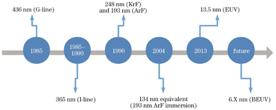
Fig. 1. Trend for the development of lithographic light sources regarding wavelength
![Schematic of the main optical components in an EUV lithography system[30]](/richHtml/zgjg/2024/51/7/0701010/img_02.jpg)
Fig. 2. Schematic of the main optical components in an EUV lithography system[30]
Fig. 3. Schematic view of Bragg diffraction for PMMs
Fig. 4. Real and imaginary parts of the refractive index at 6.7 nm for typical elements (original data obtained from Lawrence Berkeley National Laboratory)[38]
Fig. 5. Calculated results of La/B4C multilayers. (a) Reflectivity curve; (b) curve of reflectivity changing with number of periods; (c) curve of reflectivity variation with substrate roughness
Fig. 6. Calculated results of La/B4C multilayers. (a) Variation of central wavelength of multilayers with different periodic thicknesses; (b) variation of peak reflectivity of multilayers with different interface widths
Fig. 7. Schematic of La/B4C multilayers with barrier layer of carbon[55]. (a) Structures of La/B4C with carbon barrier layer inserted on different interfaces; (b) zoomed-in depth profiles of La+ measured by using TOF-SIMS (reprinted and adapted from Ref. [55] with permission from Elsevier)
Fig. 8. Experiments on the nitridation of La/B interface[7]. (a) Schematic of La/B-based multilayer prepared by using the delayed nitridation method; (b) calculated peak reflectivity for LaN/B multilayers, with BN and LaB6 as interlayers on the LaN-on-B interface (adapted with permission from Ref. [7] © The Optical Society)
Fig. 9. Annealing experiments for La/B4C and LaN/B4C multilayers[65]. (a) Period thicknesses of the La/B4C and LaN/B4C multilayer, for annealing temperatures up to 800 ℃; (b) EUV reflectance curves of the La/B4C multilayer right after deposition, and after annealing to 400 ℃ and 800 ℃, respectively; (c) EUV reflectance curves of the LaN/B4C multilayer right after deposition, and after annealing to 400 ℃ and 800 ℃, respectively (reprinted and adapted from Ref. [65] with permission from Elsevier)
|
Table 1. Advantages and disadvantages of different BEUV light sources
|
Table 2. Summary of relevant parameters for BEUV multilayers


Set citation alerts for the article
Please enter your email address

© Copyright 2018-2021 | Chinese Laser Press. All Rights Reserved 沪ICP备15018463号-20