• NUCLEAR TECHNIQUES
  • Vol. 45, Issue 11, 110402 (2022)
Yichao MA1, Liangyi WANG1, Haiyun TENG2、*, and Junguo JIANG1
Author Affiliations
  • 1Shaanxi University of Science & Technology, Xi'an 710021, China
  • 2Institute of High Energy Physics, Chinese Academy of Sciences, Dongguan 523000, China
  • show less
    DOI: 10.11889/j.0253-3219.2022.hjs.45.110402 Cite this Article
    Yichao MA, Liangyi WANG, Haiyun TENG, Junguo JIANG. Design of a TDC chip based on 0.18 μm SMIC technology[J]. NUCLEAR TECHNIQUES, 2022, 45(11): 110402 Copy Citation Text show less
    Diagram of TDC chip structure
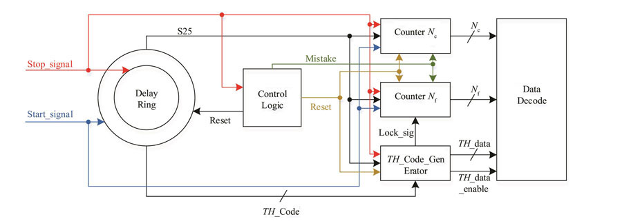
    Fig. 1. Diagram of TDC chip structure
    Differential delay chain TDC
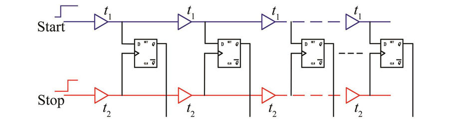
    Fig. 2. Differential delay chain TDC
    Differential delay ring TDC
    Fig. 3. Differential delay ring TDC
    Diagram of judgment unit combination(a) TDC first loop operation, (b) TDC second loop operation
    Fig. 4. Diagram of judgment unit combination(a) TDC first loop operation, (b) TDC second loop operation
    Sequence diagram of differential ring TDC
    Fig. 5. Sequence diagram of differential ring TDC
    Structure diagram of arbiter (a) Rise edge arbiter, (b) Falling edge arbiter
    Fig. 6. Structure diagram of arbiter (a) Rise edge arbiter, (b) Falling edge arbiter
    Operating cycle of arbiter A
    Fig. 7. Operating cycle of arbiter A
    Unexpected "01" conversion of arbiter B
    Fig. 8. Unexpected "01" conversion of arbiter B
    The sequence diagram shows that the register group filters out the false "01" at the falling edge (a) Fake "01" sequence diagram, (b) Sequence diagram after filtering fake "01"
    Fig. 9. The sequence diagram shows that the register group filters out the false "01" at the falling edge (a) Fake "01" sequence diagram, (b) Sequence diagram after filtering fake "01"
    Sequence diagram of B1 (a) and B2 (b)
    Fig. 10. Sequence diagram of B1 (a) and B2 (b)
    Chip layout
    Fig. 11. Chip layout
    TDC chip diagram
    Fig. 12. TDC chip diagram
    Calibration curve of delay ring
    Fig. 13. Calibration curve of delay ring
    Time accuracy of TDC
    Fig. 14. Time accuracy of TDC
    Comparison of local time difference
    Fig. 15. Comparison of local time difference
    Comparison of overall time difference
    Fig. 16. Comparison of overall time difference
    Counts of each TDC delay bin
    Fig. 17. Counts of each TDC delay bin
    DNL test results
    Fig. 18. DNL test results
    INL test results
    Fig. 19. INL test results

    参考文献

    Reference

    工艺

    Technology

    面积

    Area / μm2

    分辨率

    Resolution / ps

    时钟频率

    Clock frequency / MHz

    功耗

    Power loss / mW

    [1]0.11 μm CMOS600×3 00051.7600<100
    [2]SMIC 0.18 μm CMOS120×12032125
    [3]0.13 μm GSMC300×40701.36
    [6]0.13 μm CMOS57
    [17]0.18 μm CMOS160<8
    本文 This paper0.18 μm SMIC1 350×1 35017250
    Table 1. Comparison of TDC chips with different designs
    Yichao MA, Liangyi WANG, Haiyun TENG, Junguo JIANG. Design of a TDC chip based on 0.18 μm SMIC technology[J]. NUCLEAR TECHNIQUES, 2022, 45(11): 110402
    Download Citation