Abstract
Self-imaging is an important function for signal transport, distribution, and processing in integrated optics, which is usually implemented by multimode interference or diffractive imaging process. However, these processes suffer from the resolution limit due to classical wave propagation dynamics. We propose and demonstrate subwavelength optical imaging in one-dimensional silicon waveguide arrays, which is implemented by cascading straight and curved waveguides in sequence. The coupling coefficient between the curved waveguides is tuned to be negative to reach a negative dispersion, which is an analog to a hyperbolic metamaterial with a negative refractive index. Therefore, it endows the waveguide array with a superlens function as it is connected with a traditional straight waveguide array with positive dispersion. With a judiciously engineered cascading silicon waveguide array, we successfully show the subwavelength self-imaging process of each input port of the waveguide array as the single point source. Our approach provides a strategy for dealing with optical signals at the subwavelength scale and indicates functional designs in high-density waveguide integrations.1 Introduction
Precisely manipulating the optical field at the subwavelength scale is vital both in current imaging technology and on-chip photonic integrations. In pursuing super-resolution imaging, a striking design of a superlens based on negative index metamaterials (NIM) has been proposed;1–6 it is a revolutionary change in principle and quite different from the other strategies, such as fluorescence microscopy7–10 and structured light microscopy.11–13 To circumvent the extreme difficulties in achieving the initially proposed NIM with negative permeability and permittivity, hyperbolic metamaterials were proposed in which multilayered metal–dielectric structures and metallic nanowires arrays were designed for two kinds of hyperbolic dispersions.14–19 Unfortunately, these designs for superlens imaging remain unsatisfactory due to insurmountable manufacturing challenges and huge losses from impedance mismatch at the interface between these NIMs and a positive background. Therefore, demonstrations of a superlens in the optical regime were rarely reported.6,17–19
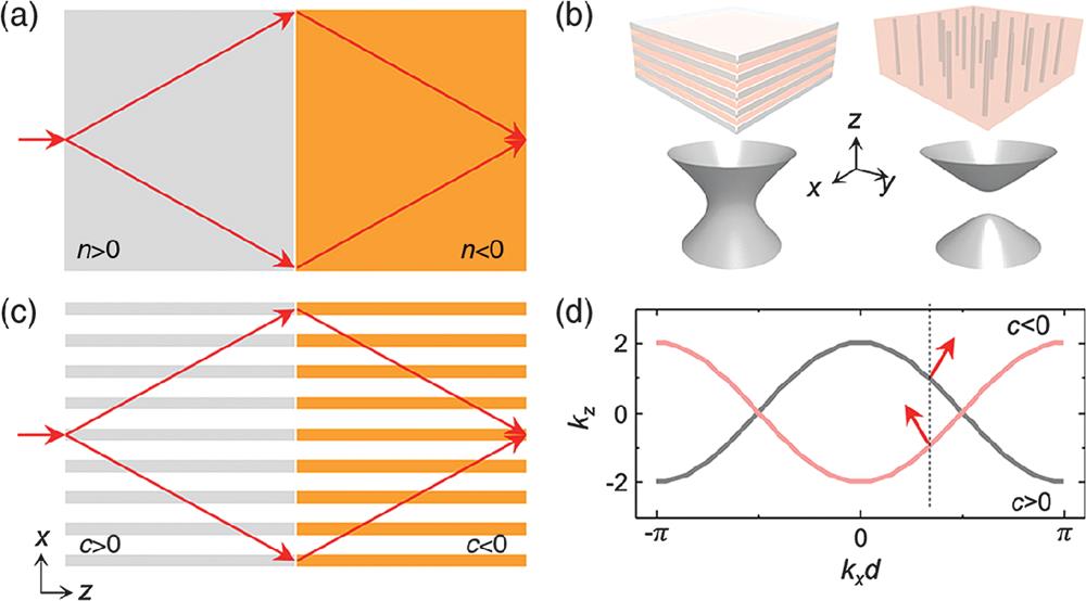
On the other hand, photonic waveguide arrays are widely used for the flexible control of light.20–33 Negative refraction, deep-subwavelength focusing, and reconstruction of initial state have been demonstrated.21–29 In fact, a waveguide array bears similarities with metamaterials as its lattice is much smaller than the wavelength in the effective medium regime. For example, the multilayer nanofilms or the arrayed-nanorod metamaterials [Fig. 1(b)] can be treated as planar [one-dimensional (1-D)] or cylindrical [two-dimensional (2-D)] waveguides arrays. It is particularly noteworthy that the coupling between the nanofilms or nanorods plays an important role in constructing the special dispersion since they are closely packed together. Therefore, it is quite possible to use the waveguides with controlled coupling to mimic the hyperbolic metamaterials with an effective negative index. By doing this, structures can be greatly simplified while many of their unusual properties and functionalities can be preserved, for example, imaging beyond the diffraction limit.

Figure 1.Superlens design with cascaded waveguides. (a) Negative refractive index material for superlens imaging. (b) Examples of hyperbolic metamaterials: multilayered metal–dielectric structure and nanorod arrays (top panel) and isofrequency surfaces of extraordinary waves in hyperbolic metamaterials (bottom panel). (c) Compensated positive and negative coupling in waveguide array for superlensing. (d) Dispersion relation for positive and negative coupling. The red arrows indicate the energy flow.
In this paper, we propose a cascaded straight and curved 1-D silicon waveguide array to access subwavelength self-imaging, where the curved waveguides array works as a negative index material with a well-engineered negative dispersion,32 while the straight part acts as normal positive index material. It is noted that the directly cascaded waveguides have almost the same propagation constant, which gives rise to the perfect impedance matching condition and greatly prohibits the scattering loss on the interface. In the experiments, different input ports of the waveguide array are illuminated as point sources and well reconstructed with the dimension smaller than through the light evolutions inside the cascaded waveguides. By contrast, in the uniform straight and curved waveguide cases, the optical field propagates in the well-known discrete diffractions with dispersed field distributions at output ports. Because waveguides are packed in the subwavelength dimension, the imaging process breaks the diffraction limit with respect to the free-space wavelength, which offers a powerful means of manipulating the optical field in the subwavelength scale by coupled waveguides. In addition, the capability of restoring the input signal provides a practical solution for high-density silicon photonic integration with low crosstalk.34,35
Sign up for Advanced Photonics TOC. Get the latest issue of Advanced Photonics delivered right to you!Sign up now
2 Design of One-Dimensional Superlens by Cascaded Waveguides
Figure 1(c) shows the scheme of a superlens constructed by cascaded waveguide arrays. We propose two sets of coupled optical waveguide arrays in series with the same period and different signs of the coupling coefficient. One is positive (), and the other is negative (). Using coupled-mode theory (CMT), the dispersion relation is , where is the spatial momentum in the direction [see Fig. 1(d)]. The red arrows indicate the energy flows. It is clear that the incident beam will be negatively refracted at the interface of the positive and negative coupled waveguides regions. To realize the negative coupling, sinusoidally curved waveguides are designed with the transverse oscillation as a function of propagation distance (in direction) as , where is the modulation period and is the oscillation amplitude [see Fig. 2(e)]. The optical field propagation within the curved waveguide array can be described by the CMT in the tight-binding approximation where enumerates the waveguides, denotes the optical field in the ’th waveguide, is the waveguide position, is the refractive index of the substrate, and denotes the coupling coefficients between the waveguides in a straight array (i.e., ) for a certain distance (). The effective coupling coefficient of the sinusoidally curved waveguides is given as33where is the lowest-order Bessel function of the first kind. is the dimensionless optical frequency. The effective coupling coefficient can be tuned by changing the modulation parameters ( and ) or the optical frequency (). Here, we consider the change of modulation amplitude without losing the impedance matching condition of the interface. The red curve in Fig. 2(b) displays the theoretically calculated as a function of (here, , , , and ); it is evident that the positive and negative couplings can be achieved by selecting a different .
Figure 2.Simulation results in 1-D silicon waveguide arrays. (a) Coupling coefficient as a function of the period of waveguides, where the red dot indicates the period we selected in our modeling. (b) Theoretical and simulated effective coupling coefficient as a function of modulation amplitude , where the red and black dots indicate the parameters of waveguides we selected in our modeling. Morphology of Si waveguide array with 13 (c) straight waveguides, (e) sinusoidally curved waveguides, and (g) cascaded waveguides, and their corresponding results of the simulated field evolution in (d), (f), and (h), respectively. Simulated signal results of “0”/“1” coded signal transmission through (i) straight, (j) curved, and (k) cascaded waveguide arrays. The output in cascaded waveguides perfectly reproduces the input signal, while the straight and curved waveguides give rise to a chaotic output signal.
According to the above considerations, we constructed the silicon waveguide arrays and employed a commercial finite-element analysis solver (COMSOL Multiphysics 5.3) for full-wave simulations. Each waveguide in the array is defined by silicon with a refractive index at , width , and height , lying on a sapphire substrate (), and in the air background. According to these parameters, only the fundamental mode is accommodated in the silicon waveguide at with a propagation constant of ( is the wave vector in free space). In our simulation, we use the open boundary condition (i.e., scattering boundary condition in COMSOL Multiphysics 5.3) and fundamental transverse electric () mode as the excitation. Figure 2(a) shows the simulated coupling coefficient as a function of the straight waveguides distance (center-to-center distance); the coupling coefficient is a positive value that decreases as the distance increases. Here, we fixed the period of waveguides to (waveguide gap ), corresponding to for straight waveguides (i.e., ). For the curved waveguides, when the modulation amplitude increases with a fixed modulation period , the effective coupling decreases and tends to be negative [see the blue curve in Fig. 2(b)]. Here, the simulated maximum is set as to avoid a big scattering loss for a larger . It should be noted that the simulated effective coupling coefficient (blue curve) deviates from the theory (red curve) in the large region. This is because Eq. (2) is an approximate expression in the small curvature condition. Actually, a slowly varying bending profile, the nearest-neighbor tight-binding approximation, and a weak refractive index change of waveguides from the substrate index are required to derive Eq. (2). However, our simulation setup of high-density silicon waveguides certainly breaks these approximations and leads to the differences. Despite the deviation, the crucial effect of the negative coupling by curved waveguides is still retained in our case. According to the simulation results, 13 waveguides are designed in the arrays both for the straight () and curved () ones with corresponding coupling coefficients of . Figure 2(g) shows the cascaded waveguide arrays by connecting each waveguide straightforwardly. To provide direct comparisons, simple straight and curved waveguide arrays were also investigated, as shown in Figs. 2(c) and 2(e).
Figures 2(d), 2(f), and 2(h) show the simulated results of light propagations within -long silicon waveguides of straight, curved, and cascaded samples, respectively, with the excitation of a single waveguide at the center as the input signal. The well-known discrete diffraction behaviors20 are observed in both the positively and negatively coupled waveguides, in which light spreads toward two sides as it propagates [see Figs. 2(d) and 2(f)]. It is also confirmed that, in the curved sample, the negative coupling only affects the coupling phase of the evolution fields and intensity distributions evolution remains almost the same as for the positive dispersion case. For the cascaded sample, the light first undergoes the discrete diffraction in the straight part and converges in an inverse process of discrete diffraction in the curved part. As a result, the power of the optical field remains localized around the center waveguide at the outputs, indicating a self-imaging function. This revival process is attributed to the phase changes of the field coupling with opposite coupling strength. It should be noted that the period of waveguides () is beyond the diffraction limit () with respect to the free space wavelength. The cascaded waveguide array indeed works as a superlens for subdiffraction imaging. Furthermore, we find that the self-imaging effect can be used to transmit an arbitrarily complex signal by such a waveguide system with subwavelength resolution. To verify this, further simulations were performed on straight, curved, and cascaded waveguides samples with multiple ports input as an arbitrary signal [i.e., (1010011010010), here “1”/“0” represents with/without light input], and the results are shown in Figs. 2(i)–2(k), respectively. As expected, the output signal in cascaded waveguides is exactly the same as the input revealing a subwavelength image, while for the straight and curved waveguides the output signals are totally chaotic. Since the signal transmission in high-density photonic integration has always been the pursuit of people working in this field, this cascaded waveguide array suggests a strategy for high-density photonic integration.
3 Experimental Results
In designing the experimental samples, each waveguide of the array is connected with two grating couplers ( and ) by taped waveguides from the two ends, where represents the coupler number, [see Fig. 3(a)]. Therefore, it is easy to individually excite a particular waveguide in the input ports and analyze the propagation in the output ports. There are three samples (straight, curved, and cascaded waveguides) in the center with the same lengths of . The designed parameters are , , and . The experimental samples are fabricated in a silicon wafer on a sapphire substrate using E-beam lithography with AR-N 7520 resists and an inductively coupled plasma etching process, which includes the waveguide array and extended grating couplers. The scanning electron microscopy (SEM) images of the fabricated devices are shown in Fig. 3(b). The coupling in and out processes are imaged by a near-infrared camera (Xeva-1.7-320) through a microscope objective.
Figure 3.Experimental results. (a) Schematics of the experimental samples with three enlarged pictures showing three different waveguide arrays. (b) SEM images of the fabricated cascaded samples. (c)–(e) CCD recorded optical propagation from input () to output through (c) straight, (d) curved, and (e) cascaded waveguide arrays. (f)–(j) Experimental results with different input port (, , , , and ) for cascaded waveguide arrays. The bar diagrams in (c)–(j) in bottom panels display the extracted data of field intensity from output ports, where the input ports of signal are indicated by red arrows.
In the experiments, we first input the light into the center waveguide by focusing the laser () to the grating coupler (i.e., ) for these three samples. The transmitted signals can be observed from another end of the grating coupler (i.e., ). Figures 3(c)–3(e) show the charge-coupled device (CCD)-recorded optical propagation from input to output through the three samples, respectively. It is clear that there are bright spots from the expected output ports () for the cascaded samples showing excellent imaging function. However, for cases of straight and curved samples, most of the optical field spreads into the side-lobes with little remaining at the center, definitely showing the discrete diffraction process. In addition, the spreading degrees of these two uniform samples are almost the same, indicating almost identical coupling strength despite different signs. In addition, we also input the light in the center grating coupler connected to the curved waveguides (i.e., ) for the cascaded sample and observed the same result with bright spots in the expected output ports () [see Fig. 3(f)], indicating a reciprocal imaging process.
To further demonstrate the imaging function, different input ports were illuminated in a controlled way, as for example shown in Figs. 3(g)–3(j), for the input ports of , , , and , respectively. The bright spots from the expected output ports (, , , and ) are evidently observed, revealing the exact high-quality point-to-point imaging process with no crosstalk to other output ports. It should be mentioned that, though the designed period is at wavelength of 1550 nm according to the simulations, the fabricated samples have a shrinking period to due to fabrication imperfections, which causes a blueshift of the working wavelength (1450 nm). All imaging resolutions are beyond the diffraction limit (), and the superlens function of subdiffraction-limited imaging is well demonstrated in the experiments.
4 Conclusion
We experimentally demonstrated optical self-imaging beyond the resolution limit in a 1-D silicon waveguide array. By connecting straight and curved waveguides, perfect self-imaging of an initial input state without crosstalk is realized in a high-density configuration. This design is implemented by tuning the coupling in the curved waveguides to be negative, mimicking the negative index material. Note that the subwavelength imaging can also be realized by plasmonics and metamaterials designs, such as plasmonic lenses36 and hyperlenses.37 Compared with these designs, our scheme has advantages in lower loss, easier fabrication requirements, and a naturally satisfied impedance matching condition. In principle, this coupled waveguide array system can be extended to a two-dimensional lattice to achieve a real imaging lens, though there would be more challenges in nanofabrications. Nevertheless, our approach provides a practical solution for efficient subwavelength self-imaging in on-chip optical signal routings, which is important in high-density photonic integrations.
References
[1] J. B. Pendry. Negative refraction makes a perfect lens. Phys. Rev. Lett., 85, 3966-3969(2000).
[2] M. C. K. Wiltshire et al. Microstructured magnetic materials for RF flux guides in magnetic resonance imaging. Science, 291, 849-851(2001).
[3] R. A. Shelby, D. R. Smith, S. Schultz. Experimental verification of a negative index of refraction. Science, 292, 77-79(2001).
[4] A. Grbic, G. V. Eleftheriades. Overcoming the diffraction limit with a planar left-handed transmission-line lens. Phys. Rev. Lett., 92, 117403(2004).
[5] D. R. Smith, J. B. Pendry, M. C. K. Wiltshire. Metamaterials and negative refractive index. Science, 305, 788-792(2004).
[6] N. Fang et al. Sub–diffraction-limited optical imaging with a silver superlens. Science, 308, 534-537(2005).
[7] W. Denk, J. Strickler, W. Webb. Two-photon laser scanning fluorescence microscopy. Science, 248, 73-76(1990).
[8] S. W. Hell, J. Wichmann. Breaking the diffraction resolution limit by stimulated emission: stimulated-emission-depletion fluorescence microscopy. Opt. Lett., 19, 780-782(1994).
[9] J. W. Lichtman, J.-A. Conchello. Fluorescence microscopy. Nat. Meth., 2, 910-919(2005).
[10] B. Huang, M. Bates, X. Zhuang. Super-resolution fluorescence microscopy. Ann. Rev. Biochem., 78, 993-1016(2009).
[11] M. G. L. Gustafsson. Surpassing the lateral resolution limit by a factor of two using structured illumination microscopy. J. Microsc., 198, 82-87(2000).
[12] L. Schermelleh et al. Sub-diffraction multicolor imaging of the nuclear periphery with 3D structured illumination microscopy. Science, 320, 1332-1336(2008).
[13] R. Fiolka et al. Time-lapse two-color 3D imaging of live cells with doubled resolution using structured illumination. Proc. Natl. Acad. Sci. U. S. A., 109, 5311-5315(2012).
[14] D. R. Smith, D. Schurig. Electromagnetic wave propagation in media with indefinite permittivity and permeability tensors. Phys. Rev. Lett., 90, 077405(2003).
[15] A. Poddubny et al. Hyperbolic metamaterials. Nat. Photonics, 7, 948-957(2013).
[16] J. Yao et al. Optical negative refraction in bulk metamaterials of nanowires. Science, 321, 930(2008).
[17] I. I. Smolyaninov, Y.-J. Hung, C. C. Davis. Magnifying superlens in the visible frequency range. Science, 315, 1699-1701(2007).
[18] Z. Liu et al. Far-field optical hyperlens magnifying sub-diffraction-limited objects. Science, 315, 1686(2007).
[19] J. Rho et al. Spherical hyperlens for two-dimensional sub-diffractional imaging at visible frequencies. Nat. Commun., 1, 143(2010).
[20] D. N. Christodoulides, F. Lederer, Y. Silberberg. Discretizing light behaviour in linear and nonlinear waveguide lattices. Nature, 424, 817-823(2003).
[21] L. Verslegers et al. Deep-subwavelength focusing and steering of light in an aperiodic metallic waveguide array. Phys. Rev. Lett., 103, 033902(2009).
[22] Y. Liu, X. Zhang. Metasurfaces for manipulating surface plasmons. Appl. Phys. Lett., 103, 141101(2013).
[23] E. Verhagen. Three-dimensional negative index of refraction at optical frequencies by coupling plasmonic waveguides. Phys. Rev. Lett., 105, 223901(2012).
[24] U. Peschel, T. Pertsch, F. Lederer. Optical Bloch oscillations in waveguide arrays. Opt. Lett., 23, 1701-1703(1998).
[25] R. Iwanow et al. Discrete Talbot effect in waveguide arrays. Phys. Rev. Lett., 95, 053902(2005).
[26] S. Longhi et al. Observation of dynamic localization in periodically curved waveguide arrays. Phys. Rev. Lett., 96, 243901(2006).
[27] S. Longhi. Image reconstruction in segmented waveguide arrays. Opt. Lett., 33, 473-475(2008).
[28] A. Szameit et al. Image reconstruction in segmented femtosecond laser-written waveguide arrays. Appl. Phys. Lett., 93, 181109(2008).
[29] A. Szameit et al. Inhibition of light tunneling in waveguide arrays. Phys. Rev. Lett., 102, 153901(2009).
[30] W. Song et al. Breakup and recovery of topological zero modes in finite non-Hermitian optical lattices. Phys. Rev. Lett., 123, 165701(2019).
[31] B. Xu, T. Li, S. Zhu. Simulation of massless Dirac dynamics in plasmonic waveguide arrays. Opt. Express, 26, 13416-13424(2018).
[32] S. Longhi. Quantum-optical analogies using photonic structures. Laser Photonics Rev., 3, 243-261(2008).
[33] J. M. Zeuner et al. Optical analogues for massless Dirac particles and conical diffraction in one dimension. Phys. Rev. Lett., 109, 023602(2012).
[34] W. Song et al. High-density waveguide superlattices with low crosstalk. Nat. Commun., 6, 7027(2015).
[35] R. Gatdula et al. Guiding light in bent waveguide superlattices with low crosstalk. Optica, 6, 585-591(2019).
[36] Z. Liu et al. Focusing surface plasmons with a plasmonic lens. Nano Lett., 5, 1726-1729(2005).
[37] D. Lu, Z. Liu. Hyperlenses and metalenses for far-field super-resolution imaging. Nat. Commun., 3, 1205(2012).