• Advanced Photonics
  • Vol. 2, Issue 3, 036001 (2020)
Wange Song1、2, Hanmeng Li1、2, Shenglun Gao1、2, Chen Chen1、2, Shining Zhu1、2, and Tao Li1、2、*
Author Affiliations
  • 1Nanjing University, College of Engineering and Applied Sciences, National Laboratory of Solid State Microstructures, Key Laboratory of Intelligent Optical Sensing and Integration, Jiangsu Key Laboratory of Artificial Functional Materials, Nanjing, China
  • 2Collaborative Innovation Center of Advanced Microstructures, Nanjing, China
  • show less
    DOI: 10.1117/1.AP.2.3.036001 Cite this Article Set citation alerts
    Wange Song, Hanmeng Li, Shenglun Gao, Chen Chen, Shining Zhu, Tao Li. Subwavelength self-imaging in cascaded waveguide arrays[J]. Advanced Photonics, 2020, 2(3): 036001 Copy Citation Text show less
    Superlens design with cascaded waveguides. (a) Negative refractive index material for superlens imaging. (b) Examples of hyperbolic metamaterials: multilayered metal–dielectric structure and nanorod arrays (top panel) and isofrequency surfaces of extraordinary waves in hyperbolic metamaterials (bottom panel). (c) Compensated positive and negative coupling in waveguide array for superlensing. (d) Dispersion relation for positive and negative coupling. The red arrows indicate the energy flow.
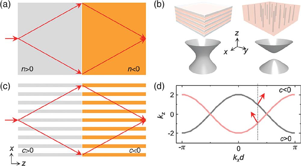
    Fig. 1. Superlens design with cascaded waveguides. (a) Negative refractive index material for superlens imaging. (b) Examples of hyperbolic metamaterials: multilayered metal–dielectric structure and nanorod arrays (top panel) and isofrequency surfaces of extraordinary waves in hyperbolic metamaterials (bottom panel). (c) Compensated positive and negative coupling in waveguide array for superlensing. (d) Dispersion relation for positive and negative coupling. The red arrows indicate the energy flow.
    Simulation results in 1-D silicon waveguide arrays. (a) Coupling coefficient as a function of the period of waveguides, where the red dot indicates the period we selected in our modeling. (b) Theoretical and simulated effective coupling coefficient ceff as a function of modulation amplitude A, where the red and black dots indicate the parameters of waveguides we selected in our modeling. Morphology of Si waveguide array with 13 (c) straight waveguides, (e) sinusoidally curved waveguides, and (g) cascaded waveguides, and their corresponding results of the simulated field evolution in (d), (f), and (h), respectively. Simulated signal results of “0”/“1” coded signal transmission through (i) straight, (j) curved, and (k) cascaded waveguide arrays. The output in cascaded waveguides perfectly reproduces the input signal, while the straight and curved waveguides give rise to a chaotic output signal.
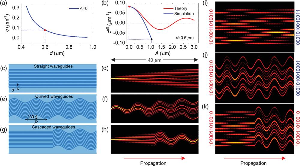
    Fig. 2. Simulation results in 1-D silicon waveguide arrays. (a) Coupling coefficient as a function of the period of waveguides, where the red dot indicates the period we selected in our modeling. (b) Theoretical and simulated effective coupling coefficient ceff as a function of modulation amplitude A, where the red and black dots indicate the parameters of waveguides we selected in our modeling. Morphology of Si waveguide array with 13 (c) straight waveguides, (e) sinusoidally curved waveguides, and (g) cascaded waveguides, and their corresponding results of the simulated field evolution in (d), (f), and (h), respectively. Simulated signal results of “0”/“1” coded signal transmission through (i) straight, (j) curved, and (k) cascaded waveguide arrays. The output in cascaded waveguides perfectly reproduces the input signal, while the straight and curved waveguides give rise to a chaotic output signal.
    Experimental results. (a) Schematics of the experimental samples with three enlarged pictures showing three different waveguide arrays. (b) SEM images of the fabricated cascaded samples. (c)–(e) CCD recorded optical propagation from input (I0) to output through (c) straight, (d) curved, and (e) cascaded waveguide arrays. (f)–(j) Experimental results with different input port (II0, I−6, I−4, I1, and I6) for cascaded waveguide arrays. The bar diagrams in (c)–(j) in bottom panels display the extracted data of field intensity from output ports, where the input ports of signal are indicated by red arrows.
    Fig. 3. Experimental results. (a) Schematics of the experimental samples with three enlarged pictures showing three different waveguide arrays. (b) SEM images of the fabricated cascaded samples. (c)–(e) CCD recorded optical propagation from input (I0) to output through (c) straight, (d) curved, and (e) cascaded waveguide arrays. (f)–(j) Experimental results with different input port (II0, I6, I4, I1, and I6) for cascaded waveguide arrays. The bar diagrams in (c)–(j) in bottom panels display the extracted data of field intensity from output ports, where the input ports of signal are indicated by red arrows.
    Wange Song, Hanmeng Li, Shenglun Gao, Chen Chen, Shining Zhu, Tao Li. Subwavelength self-imaging in cascaded waveguide arrays[J]. Advanced Photonics, 2020, 2(3): 036001
    Download Citation