
Yanxin Jin, Qiuqi Wu, Chaoyang Tang, Wenjun Cao, Xuda Guo, Jiwei Hou. Construction of V2O5/SnO2 Nanofiber Heterojunctions and Their Optoelectronic Properties[J]. Acta Optica Sinica, 2024, 44(2): 0204002
- Acta Optica Sinica
- Vol. 44, Issue 2, 0204002 (2024)
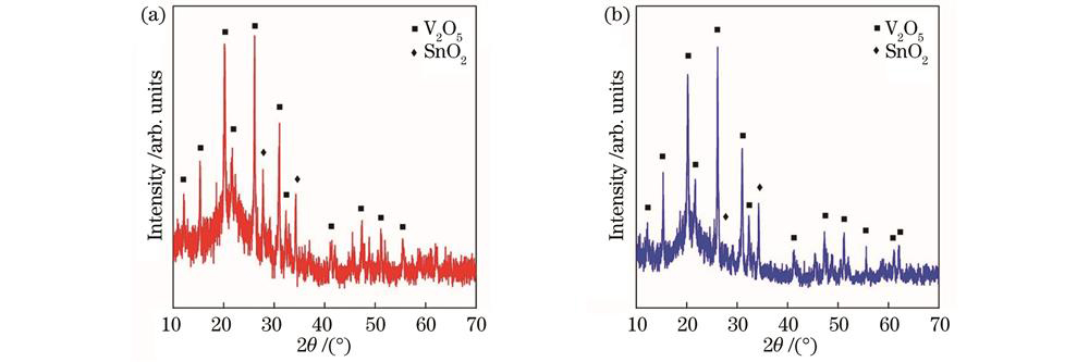
Fig. 1. XRD images of electrostatically spun-grown V2O5/SnO2 nanofiber heterostructures heat-treated in different atmospheres. (a) Heat-treated in air atmosphere; (b) heat-treated in argon atmosphere
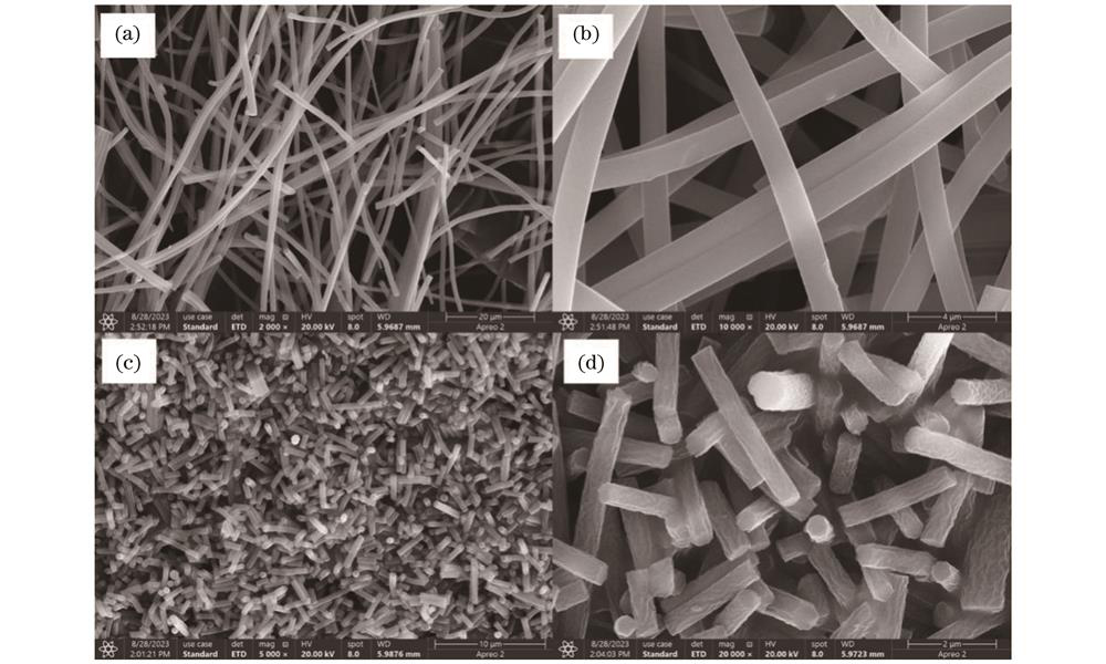
Fig. 2. SEM images of heterogeneous structure of V2O5/SnO2 nanofibers heat-treated in different atmospheres. (a) SEM image of heat-treated in argon atmosphere at low magnification; (b) SEM image of heat-treated in argon atmosphere at high magnification; (c) SEM image of heat-treated in air atmosphere at low magnification; (d) SEM image of heat-treated in air atmosphere at high magnification
Fig. 3. EDS analysis images of heterostructure of V2O5/SnO2 nanofibers obtained by heat treatment in air atmosphere. (a) Typical SEM image; (b) EDS image; (c) distribution of element C; (d) distribution of element O; (e) distribution of element V; (f) distribution of element Sn
Fig. 4. TEM images of heterostructure of V2O5/SnO2 nanofibers obtained by heat treatment in argon atmosphere, where dashed lines mark demarcation line of core-shell structure. (a) TEM image at low magnification; (b) TEM image at intermediate magnification; (c) TEM image at high magnification
Fig. 5. XPS profiles of heterostructures of V2O5/SnO2 nanofibers obtained by heat treatment in air atmosphere. (a) XPS full spectrum; (b) binding energy of V2p; (c) binding energy of Sn3d; (d) binding energy of C1s
Fig. 6. Single V2O5/SnO2 nanofiber heterojunction photodetector. (a) Schematic diagram of photodetector; (b) physical photo of photodetector
Fig. 7. I-V curves of two photodetectors under laser irradiation and dark conditions. (a) V2O5/SnO2 nanofiber heterojunction device; (b) V2O5 nanofiber device
Fig. 8. I-V curves of two photodetectors under different laser irradiation powers. (a) V2O5/SnO2 nanofiber heterojunction device; (b) V2O5 nanofiber device
Fig. 9. Photocurrent versus time for different laser irradiations with a bias voltage of 3.0 V. (a) Laser irradiation with a wavelength of 405 nm and a power of 123 mW; (b) laser irradiation with a wavelength of 532 nm and a power of 92 mW
Fig. 10. Individual cyclic dynamic photocurrents of two photodetectors under laser irradiation with a wavelength of 405 nm and a power of 123 mW when bias voltage is 3.0 V. (a) V2O5/SnO2 nanofiber heterojunction device; (b) V2O5 nanofiber device
Fig. 11. Schematic illustration of type Ⅱ band arrangement formed by V2O5/SnO2 heterojunction

Set citation alerts for the article
Please enter your email address
© Copyright 2018-2021 | Chinese Laser Press. All Rights Reserved 沪ICP备15018463号-20