Abstract
To simultaneously obtain high-resolution multi-wavelength (from visible to near infrared) tomographic images of the solar atmosphere, a high-performance multi-wavelength optical filter has to be used in solar imaging telescopes. In this Letter, the fabrication of the multi-wavelength filter for solar tomographic imaging is described in detail. For this filter, and are used as high- and low-index materials, respectively, and the multilayer structure is optimized by commercial Optilayer software at a 7.5° angle of incidence. Experimentally, this multi-wavelength optical filter is prepared by a plasma ion-assisted deposition technique with optimized deposition parameters. High transmittance at 393.3, 396.8, 430.5, 525, 532.4, 656.8, 705.8, 854.2, 1083, and 1565.3 nm, as well as high reflectance at 500 and 589 nm are achieved. Excellent environmental durability, demonstrated via temperature and humidity tests, is also established.Over the past few years great interest has been directed to the development of high-resolution solar tomographic imagers, which are normally a configuration of ground-based solar telescopes employed for better understanding and forecasting of solar activities, such as flare, erupting prominence, coronal mass ejection, etc.[1,2]. In order to acquire valuable information on the photosphere and chromosphere of the solar atmosphere, simultaneous imaging at the multi-wavelength, ranging from visible to near infrared (IR), to select different spectral lines from different layers of the solar atmosphere is strictly required. Generally, the spectral lines can be selected for tomographic imaging of the solar atmosphere mainly include the Ca II H line (393.3 and 396.8 nm) G-band (430.5 nm), Na line (589 nm), line (656.3 nm), TiO band (705.7 nm), Ca II IR line (854.2 nm), He I line (1083 nm), Fe I line (1565.3 nm), and so on.
When preparing optical-interference coatings for the application of solar atmosphere tomographic imaging, dielectric materials with low absorption and high environmental durability are desirable. Related film properties, such as optical constants, stress, porosity, and stoichiometry, must be taken into consideration. In the spectral range from visible to near IR, dielectric oxides are the choice of materials for the fabrication of low-loss optical coatings. Among the available oxide materials, including , , MgO, , , , , ZnO, and , and have been commonly used as the low- and high-index materials[3–11]. In the past, plenty of investigations on optical and micro-structural properties of coatings combined with these two oxide materials have been implemented by various deposition techniques, such as ion beam sputtering[3], plasma ion-assisted deposition (PIAD)[8], magnetron sputtering[9], etc. In view of the particle/defect level, film stress, and manufacturing cost, PIAD is still the preferred technology for the deposition of oxide thin films with high optical performance and excellent environmental durability.
In the present work, the fabrication of a multi-wavelength visible and IR filter to be used in a solar atmosphere tomographic imager installed at a 1 m New Vacuum Solar Telescope[1] is described. The spectral requirements for the solar atmosphere tomographic imaging application are high transmittance at 393.3, 396.8, 430.5, 525, 532.4, 656.8, 705.8, 854.2, 1083, and 1565.3 nm, and high reflectance at 500 and 589 nm. To meet such requirements, an optical filter at a 7.5° angle of incidence is optimally designed with a multilayer structure of non-quarter-wave optical thickness and coated on a fused silica substrate by PIAD technology. The optical performance and environmental durability of the prepared multi-wavelength filter are evaluated.
Sign up for Chinese Optics Letters TOC. Get the latest issue of Chinese Optics Letters delivered right to you!Sign up now
Experimentally, the multi-wavelength filter is prepared with a Leybold SYRUS pro 1110 DUV planetary coating plant, consisting of an advanced plasma source (APS), two electron beam guns, and four ceramic heaters. The APS is used to bombard a growing film with argon (Ar) and oxygen () ions. In the coating process, a base pressure of approximately is ensured in the vacuum chamber by a cryopump set that provides an oil-free environment for film depositions. Fused silica () with a root-mean-square surface roughness of approximately 0.5 nm is used as the substrate. The distance between the evaporation sources and the substrate is 750 mm. Thickness uniformity across the entire coating surface is better than 99.95% using the planetary system. For film depositions, the fused silica substrate is first treated manually with alcohol and acetone in a normal laboratory environment, and then cleaned with Ar plasma formed by the APS in the vacuum chamber in order to remove potential contaminations. High-purity and grains (Merck) are used as high- and low-index materials, respectively. During film depositions, the physical thicknesses and deposition rates of thin films are controlled by a quartz crystal monitor, which is positioned at the top center of the deposition chamber. and are fabricated by the PIAD process at a substrate temperature of 200°C. The deposition rates of and films are set to 0.5 and 1.0 nm/s, respectively. High-purity (99.999%) is employed to improve the stoichiometric ratio of the thin films. The deposition parameters of the and films are summarized in Table 1. After the deposition process is finished, the sample is allowed to cool down to room temperature, and then the vacuum chamber is vented. The transmittance spectra of the prepared filter sample in the spectral range from 370 to 1600 nm are measured with a Perkin Elmer Lambda 900 spectrophotometer with a wavelength step of 1 nm. Transmittance measurements are performed at a 7.5° angle of incidence.
| Material | Temperature (°C) | Deposition rate (nm/s) | Bias voltage (V) | Discharge current (A) | Gas flow (sccm) |
|---|
| O2 | Ar |
|---|
| Ta2O5 | 200 | 0.5 | 130 | 50 | 15 | 10 |
| SiO2 | 1.0 | 140 | 5 |
Table 1. Deposition Parameters for the Ta2O5 and SiO2 Films
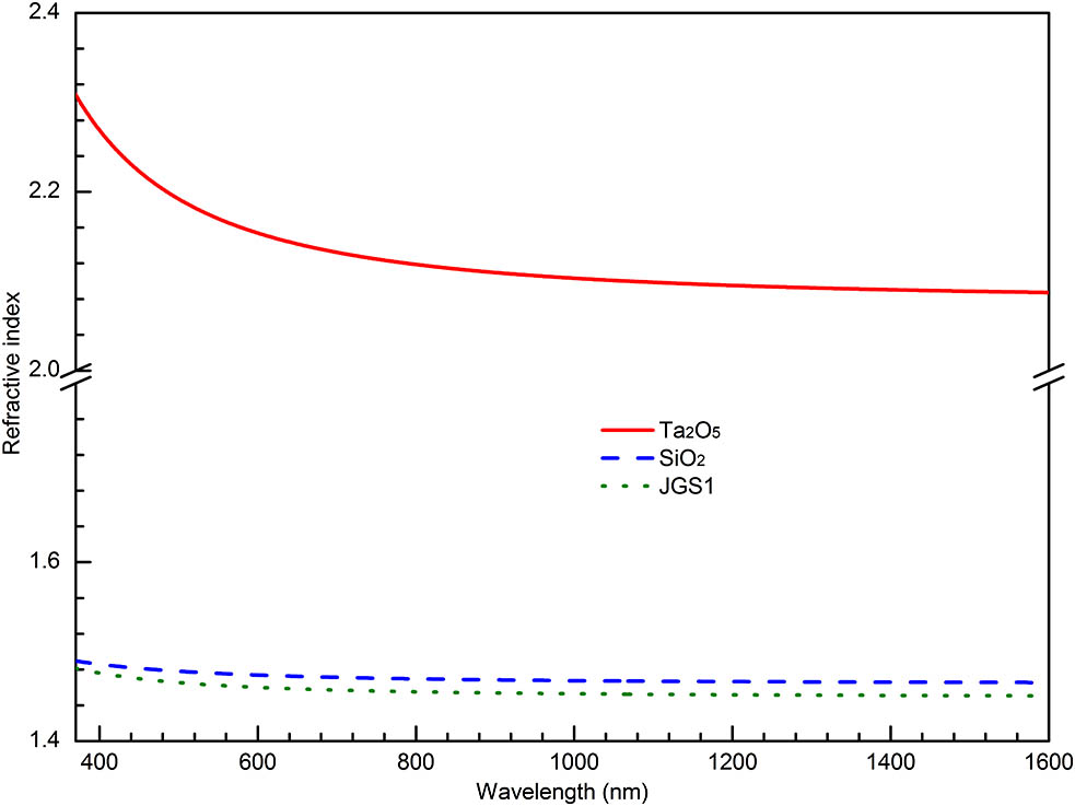
For the design and preparation of the wavelength filter, first it is important to precisely determine the refractive indexes of the and layers. Up till now, many methods have been developed for the determination of refractive indexes of optical thin films. Among them, the spectrophotometric approach is the most widely adopted method[12]. In our case, a single layer with a physical thickness of approximately 180 nm is first prepared, and its measured transmittance is employed for the refractive index determination. Thin film software OptiChar is used to fit the measured spectra to determine the refractive index and physical thickness of the single layer[13]. The initial thickness tooling factor of the layer is simultaneously determined to be 0.9154. The thickness tooling factor is defined as the ratio of actual thickness to input thickness. The determined refractive index is shown in Fig. 1. For the layer, as the refractive index difference between the film and fused silica substrate is small, the determination of the refractive index of the single layer deposited on the fused silica substrate using spectrophotometric measurements is extremely difficult. To overcome this problem, a two-layer stack with a structure of Sub/50 nm 200 nm is applied to obtain the refractive index of the layer. Thin film software OptiRE is used to fit the measured transmittance spectra to obtain the refractive index of the layer[13]. For parameter determination, and films and the fused silica substrate are assumed to be non-absorbing, as their extinction coefficients are lower than in the interested wavelength range and have negligible impact on the transmission. The refractive index versus wavelength is fitted using the Cauchy law. The initial thickness tooling factor of the layer is obtained to be 0.8734. The refractive indexes of the layer and fused silica substrate are also presented in Fig. 1. The refractive index of the film is slightly larger than that of the fused silica substrate. It is due to a high bias voltage of APS. The phenomenon was reported in Refs. [14,15]. For PIAD, a high bias voltage leads to dense films and improved environmental durability, as demonstrated by our experimental results presented below.

Figure 1.(Color online) Refractive indexes of , , and fused silica substrate for the design of a multi-wavelength filter.
Practically, the multi-wavelength filter is optimized and fabricated on both sides of the fused silica substrate. For the design of the multi-wavelength filter, the performance targets are: side A, the transmittance is larger than 98% at wavelengths of 393.3, 396.8, 430.5, 525, 532.4, 656.8, 705.8, 854.2, 1083, and 1565.3 nm, and the reflectance is larger than 98% at wavelengths of 500 and 589 nm; side B, multi-wavelength anti-reflectance coating is deposited to minimize residual (ghost) reflection, improve transmission, and compensate the mechanical stress induced by the coating at side A[16]. The transparent working wavelengths of side B are the same as those of side A. In addition, taking into consideration the feasibility and repeatability, each working wavelength has a band with a width of at least 10 nm. To meet the requirements for the high-resolution multi-wavelength simultaneous imaging system, additional narrow bandpass filters are employed. For example, the full width at half-maximum (FWHM) is about 0.5 nm for the optical filter performed at 430.5 nm. The optical layout of the imaging system and parameters for these narrow bandpass filters have been presented in Ref. [17]. The performance targets are illustrated in Fig. 2. The structure of the multi-wavelength filter is optimized with the help of a needle technique incorporated into the OptiLayer software[13]. For the design of optical coatings without thin layers, a stochastic constrained algorithm is employed. The minimum physical thickness constraints of and layers are set to 20 and 25 nm, respectively. The theoretical spectral performance and layer thicknesses of the final design are indicated in Fig. 2. The transmittance is higher than 99% in the transmitting spectral region, and the reflectance is higher than 99% at wavelengths of 500 and 589 nm.
Figure 2.(Color online) (a) Calculated transmittance of thin film on side A without backside coating. (b) Layer thickness profile of optical coating for side A. (c) Calculated transmittance of thin film for side B without backside coating. (d) Layer thickness profile of optical coating on side B.
The fabrication of the multi-wavelength filter having very thin layers is a complicated task. In our experiment, the layer thicknesses of the designed multi-wavelength filter are controlled with a quartz crystal monitor. In this case, it is crucial to precisely determinate the layer thickness tooling factor and residual error[18]. Residual error is mainly caused by the control error of the evaporator shutter and can be determined from experimental statistics. Based on previously obtained thickness tooling factors of and films, optical coating for mirror side A has been prepared. Transmittance of the one-side-coated fused silica substrate is measured and presented in Fig. 3. Obviously, the first experimental result is somewhat inconsistent with the theoretical design. To correct this inconsistence, the thickness tooling factors of both materials are further corrected with the help of OptiRE software; the residual errors are obtained from previous experimental statistics. After these corrections, an improved experimental result is obtained. The transmittance spectrum of the coating prepared under the improved process parameters is shown in Fig. 3. For the multi-wavelength filter with both sides coated, the measured and calculated transmittance curves are presented in Fig. 4. Transmittance values at visible wavelengths of 393.3, 396.8, 430.5, 525, 532.4, 656.8, and 705.8 nm are higher than 97%, and at near IR wavelengths of 854.2, 1083, and 1565.3 nm are larger than 99.5%. The reflectance value at wavelengths of 500 and 589 nm are higher than 99.5%. Good agreement between the design and experiment is obtained.
Figure 3.(Color online) Transmittance spectra of two experimental runs and theoretical design for the multi-wavelength filter coated on side A.
Figure 4.(Color online) Transmittance spectra of the two-side-coated multi-wavelength filter, and after temperature and humidity tests.
Environmental durability of the prepared multi-wavelength filter is tested on the basis of temperature and humidity requirements of the Chinese military specifications GJB150.5 A-2009 and GJB150.9 A-2009. Parameters for temperature and humidity tests are shown in Tables 2 and 3, respectively. No physical damages are observed after the temperature and humidity tests, and no coatings are removed under the adhesion test. The transmittance spectra of the prepared multi-wavelength filter after both tests are also presented in Fig. 4. There is no observable difference among these spectra. These results demonstrate that the PIAD deposited filter has excellent environmental durability in terms of high/low temperature and high humidity.
| | Temperature (°C) | Test Time (h) | Rate of Temperature Change (°C/min) |
|---|
| Temperature test | 65 | 2 | <2 |
| −40 | 2 | <2 |
Table 2. Temperature Test Parameters
| | Temperature (°C) | Relative Humidity (%) | Test Time (h) |
|---|
| Humidity test | 60 | 95 | 72 |
Table 3. Humidity Test Parameters
In conclusion, we design and prepare a complex multi-wavelength filter for solar atmosphere tomographic imaging applications. Fabrication of such a multi-wavelength filter using quartz crystal monitoring is a technical challenge due to the fact that the optical performance of this multi-wavelength filter is highly sensitive to layer thickness errors. The design and deposition of this complex many-layer filter requires the accurate determinations of refractive index, thickness tooling factor, and residual error of thin films to achieve good performance. By overcoming these difficulties in the design and fabrication process, a multi-wavelength filter with excellent optical performance and good environmental durability is successfully fabricated by PIAD for solar atmosphere tomographic imaging applications.
References
[1] C. Rao, L. Zhu, X. Rao, L. Zhang, H. Bao, L. Kong, Y. Guo, X. Ma, M. Li, C. Wang, X. Zhang, X. Fan, D. Chen, Z. Feng, X. Wang, N. Gu, Z. Wang. Chin. Opt. Lett., 13, 120101(2015).
[2] R. Volkmer, O. von der Lühe, C. Denker, S. K. Solanki, H. Balthasar, T. Berkefeld, P. Caligari, M. Collados, A. Fischer, C. Halbgewachs, F. Heidecke, A. Hofmann, M. Klvaňa, F. Kneer, A. Lagg, E. Popow, D. Schmidt, W. Schmidt, M. Sobotka, D. Soltau, K. G. Strassmeier. Astron. Nachr., 331, 624(2010).
[3] Y. Jiang, H. Liu, L. Wang, C. Jiang, Y. Ji, Y. Yang. Chin. Opt. Lett., 11, S10406(2013).
[4] C. Franke, O. Stenzel, S. Wilbrandt, S. Schröder, L. Coriand, N. Felde, A. Tünnermann. Appl. Opt., 56, 3913(2017).
[5] J. B. Oliver, C. Smith, J. Spaulding, A. L. Rigatti, B. Charles, S. Papernov, B. Taylor, J. Foster, C. W. Carr, R. Luthi, B. Hollingsworth, D. Cross. Opt. Mater. Express, 6, 2291(2016).
[6] R. Hong, J. Shao, H. He, Z. Fan. Chin. Opt. Lett., 3, 428(2005).
[7] X. Xiao, G. Dong, H. He, H. Qi, Z. Fan, J. Shao. Chin. Opt. Lett., 7, 967(2009).
[8] O. Stenzel, J. Harhausen, D. Gäbler, S. Wilbrandt, C. Franke, R. Foest, N. Kaiser. Opt. Mater. Express, 5, 2006(2015).
[9] R. Shakoury, R. R. Willey. Appl. Opt., 55, 5353(2016).
[10] K. Chen, H. Zhu, X. Yi, S. Cheng, J. Li, S. Wang, M. Lu, M. Xu, L. Ma, L. Lv. Chin. Opt. Lett., 13, 103101(2015).
[11] Y. Cui, H. Li, K. Yi, J. D. Shao. Chin. Opt. Lett., 13, 023101(2015).
[12] C. Guo, M. Kong, W. Gao, B. Li. Opt. Let., 38, 40(2013).
[13]
[14] U. Schulz, S. Jakobs, N. Kaiser. Proc. SPIE, 2776, 169(1996).
[15] T. V. Amotchkina, M. K. Trubetskov, V. Pervak, B. Romanov, A. V. Tikhonravov. Appl. Opt., 51, 5543(2012).
[16] T. V. Amotchkina, M. K. Trubetskov, Y. Pervak, L. Veisz, V. Pervak. Opt. Express, 22, 30387(2014).
[17] C. H. Rao, L. Zhu, N. T. Gu, X. J. Rao, L. Q. Zhang, H. Bao, L. Kong, Y. M. Guo, L. B. Zhong, X. A. Ma, M. Li, C. Wang, X. J. Zhang, X. L. Fan, D. H. Chen, Z. Y. Feng, X. Y. Wang, Z. Y. Wang. Astron. J., 154, 143(2017).
[18] D. M. Liu, X. J. Wang, X. H. Fu, J. Zhang, Y. G. Pan. Acta Photon. Sin., 43, 0131002(2014).