The spatial distribution of electromagnetic fields emitted from the aperture tip of a scanning near-field optical microscope (SNOM), which is called the emission pattern, depends on the geometry of the apex and the material composition of the tip’s coating. In previous works, experimental measurements of the emission pattern from the aperture tip were performed mostly in the far field. Moreover, the corresponding theoretical models were also developed based on these far-field measurements. Here, we have used the automated dual-tip SNOM to systematically characterize the emission from the aperture tip in the near field. In this regard, we have considered three different pairs of excitation and detection tips with distinct geometries. The emission patterns of the excitation tips were mapped using detection tips. Unidirectional surface plasmon polaritons (SPPs) at the surface of a gold platelet were launched by an excitation tip and measured in the near field by the detection tip. The experimental results were numerically reproduced by means of the Bethe–Bouwkamp model. This work puts into evidence the applicability of the automated dual-tip SNOM as the only available characterization technique to measure the emission from aperture tips in the near field. The reported asymmetric SPP radiation patterns can find applications in photonic integrated circuits or in biological and chemical sensing.
1. INTRODUCTION
An aperture scanning near-field optical microscope (SNOM) is an indispensable technique to study light–matter interaction with resolution beyond the diffraction limit [1]. The subwavelength aperture tip of the SNOM can behave as either a point source or point detector. The geometry and material properties of a SNOM tip’s apex determine the electromagnetic field distribution from its aperture at the apex (illumination mode) and its detection sensitivity to electric and magnetic fields (collection mode) [2,3].
In the dual-tip SNOM, prior knowledge about the polarization of the emission from the excitation aperture tip is critical to investigate polarization-sensitive near-field phenomena [4–6]. Different models have been suggested to describe the emission from aperture SNOM tips. The Bethe–Bouwkamp model is the most well known [7,8]. This model was first proposed to explain the diffraction of light through a subwavelength aperture in an infinite conducting plane. According to it, the emission from the subwavelength aperture in an infinite conducting plane corresponds to the radiation of an in-plane magnetic dipole and an out-of-plane electric dipole located at the center of the aperture. The electric dipole appears in the model only when the aperture is illuminated by a plane wave under oblique incidence.
The near-field distribution from an aperture tip was mapped for the first time using dye molecules [9]. Dye molecules behave like electric dipoles. When a dye molecule is illuminated with the aperture tip, its emission pattern corresponds to the electromagnetic field distribution from the aperture tip, projected along the molecular dipole moment. The Bethe–Bouwkamp model properly described the measured electric field distribution detected by dye molecules in the near field of the aperture tip.
Sign up for Photonics Research TOC. Get the latest issue of Photonics Research delivered right to you!Sign up now
However, the far-field angular measurements of the transmitted light through the aperture tip could not be explained by the Bethe–Bouwkamp model [10,11]. The discrepancy arose from different boundary conditions for the conical geometry of the aperture tip compared to the aperture in an infinite metallic plane. Drezet et al. developed a model that uses effective electric and magnetic dipoles with different orientations to fulfill the boundary conditions imposed by a distinct conical geometry of an aperture SNOM tip [12]. On the other hand, the emission from an aperture SNOM tip can be assumed as the radiation of a nanoantenna whose emission pattern is described by a multipole expansion method [13]. Typically, a combination of electric and magnetic dipoles is sufficient to describe the angular field distribution from the aperture tips. If the electric and magnetic dipoles cannot describe the emission pattern, the contribution of higher-order multipoles should be considered [14].
Image formation is also not trivial when aperture SNOM tips are used in the collection mode. Greffet explained the equivalence of the collection and illumination modes based on the reciprocity of electromagnetic fields [15]. The apex geometry of SNOM tips determines the dominant excited dipole moments from the aperture. Likewise, when aperture SNOM tips are used for detection, according to the reciprocity of electromagnetic fields, induced dipole moments due to scattered electric or magnetic field distributions rely on the geometry of the aperture tip [2,16–19]. Aperture tips have shown sensitivity to both electric and magnetic fields [18]. For instance, fiber tips with the apex plane parallel to the sample [20,21] and hollow pyramid probes exhibit a high sensitivity to the in-plane magnetic field [22,23]. However, a split ring tip detects out-of-plane magnetic field components [24]. In the case of gold-coated aperture tips (similar to the aperture tips used in the dual-tip SNOM measurements in this work), if the thickness of the coating enables the excitation of circularly symmetric plasmon modes, the detected signal corresponds mainly to the magnetic field intensity [2,25,26]. Nevertheless, the detection sensitivity of the aperture tip can be tuned to either the electric or magnetic field by changing the thickness of the metallic rim [21,27]. Recently, an image theory based on the reciprocity of the electromagnetic field and multipole expansion method was proposed to design SNOM tips with predefined sensitivity to the electric or magnetic field [28].
The emission from an aperture fiber tip, acting as a dipole source, can be characterized through the near-field pattern of the excited surface plasmon polaritons (SPPs) at an air–gold interface. The measured near-field patterns of the SPPs excited by the aperture tip correspond to the near-field patterns observed when the SPPs are excited by an in-plane electric or magnetic dipole. However, once asymmetric SPP patterns are observed, for some particular geometries of the aperture tip, both out-of-plane and in-plane electric or magnetic dipoles should be taken into account to describe the SPP patterns.
The polarization of the electric field at the aperture plane can be deduced from the orientation of the SPP near-field pattern [20]. An unstructured monocrystalline gold platelet with an ultrasmooth surface ensures that any asymmetry in the mapped SPP pattern is due only to the emission from the aperture fiber tip. However, it should be noted that the avoidance area, which is built up during the automated scan of a detection tip around the excitation tip, does not allow access to the entire near-field pattern. This is one of the shortcomings of the dual-tip SNOM measurement technique. Therefore, the conclusions drawn from the near-field measurements should be supported by numerical simulations.
In this work, we have shown the self-characterization capability of the dual-tip SNOM setup, which allows us to systematically investigate the polarization and emission pattern from the aperture fiber tip with arbitrary geometry at its apex. In a previous work by Klein et al., where only the polarization of the emission from the bend aperture tip was investigated, at least three scans in different directions toward the excitation tip were taken to construct one image [29]. Thus, the measurements were cumbersome, and the reproducibility of the mapped near-field patterns was challenging. However, from a technical point of view, in the current paper, the automated dual-tip SNOM enables access to more details of the electromagnetic field distribution in the near-field regime and mapping the entire near-field pattern at once. Therefore, the dual-tip SNOM introduced the self-characterization feature to study the emission from aperture tips with different geometries at the apex. To the best of our knowledge, we report for the first time a systematic analysis of the electromagnetic field distribution and the emission pattern emitted by an aperture tip as a function of its geometry. From this analysis, we demonstrate the possibility of exciting and mapping unidirectional emission patterns in the near-field regime. In particular, the dependence of the emission pattern on the geometry of the apex was not investigated previously in the near-field regime. Only in Ref. [30] did the authors assume the asymmetry of the excitation aperture tip (used as an SPP point source) to explain their experimental results. However, the effects of the tip geometry in the emission pattern were out of the scope of that paper. The unidirectional SPPs are usually excited by nanostructuring a metallic film [31–33]. The main difference of the results reported in our work is that the unidirectionality of the launched SPPs does not come from any protrusion or patterning in the metallic film. It is just a fact of the geometry of their own excitation tips. This has the important advantage of avoiding fabrication of complex geometries, minimizing possible fabrication errors, and improving compatibility with waveguides and photonic circuits. Since the near-field characterization of many nanophotonics systems relies on SNOM measurements, many applications would benefit from the self-characterization capability of the automated dual-tip SNOM and the obtained results by such a technique.
From the dual-tip SNOM measurements, we also evidenced two different features. On one hand, the bendiness determines the polarization that reaches the aperture at the apex. On the other hand, the apex’s geometry determines the excited multipole and, in turn, the electromagnetic field distribution due to emission from the aperture.
We also explain the experimental emission patterns by using the Bethe–Bouwkamp model. By comparing the attained patterns from this model with those obtained by considering the real aperture tip geometry (double truncated cone), we conclude that the Bethe–Bouwkamp model is sufficient to describe the emission from the aperture fiber tip used in the dual-tip SNOM measurements. The results of this work may find applications in biological and chemical sensing [34], photonic integrated circuits (PICs) [35,36], waveguides, ultrafast information processing in plasmonic nanocircuit components, beam splitters, multiplexers, developing robust nanometric optoelectronic components, and optical communications [32].
2. POLARIZATION CHARACTERISTIC OF BENT APERTURE FIBER TIPS
The optical response of most photonic systems is polarization dependent. Therefore, in far-field optical microscopy, the polarization of the incident beam must be determined before carrying out the experiment. Likewise, polarization-resolved measurements in the near field, using aperture SNOM tips, require knowledge of the polarization of the emitted light from their apertures [29]. An aperture SNOM tip with a bent fiber is one of the commonly used aperture probes for near-field measurements. However, determining the polarization of the emission from a bent aperture tip is not trivial. Although it is possible to control the polarization of the beam that couples to the end of the fiber tip, the polarization reaching its aperture is not always maintained, being different from the input polarization [37–40].
Far-field measurements have already been performed to study the polarization of the emission from bent fiber tips [29,37,38,41]. In fact, it was shown that the symmetry break induced by the bend along the fiber tips leads to the polarization-dependent losses in the fiber aperture tips [29,41].
However, one of the most important disadvantages of the far-field characterization of the aperture tip is that it provides no information concerning the near-field emission pattern from the aperture. This drawback can be solved using an automated dual-tip SNOM. In particular, the detection tip of the automated dual-tip SNOM can characterize the emission properties of an aperture fiber tip through the near-field pattern of the SPPs excited by the aperture tip at an air–gold interface. This is called a self-characterization capability of the automated dual-tip SNOM. The orientation of the SPP near-field pattern indicates the polarization of the electric field at the aperture plane of an excitation tip after passing through the bend of the fiber tip [29,31,42].
The described approach was followed in this work to determine the polarization of the emitted beam from the aperture at the apex of the bent fiber tip.
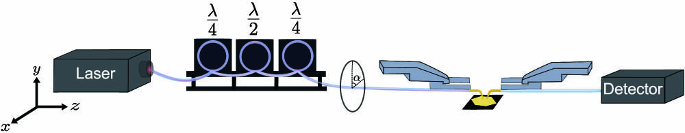
Figure 1 shows the dual-tip SNOM setup for the polarization characterization of the emission from the aperture tip in the near field. A fiber polarization controller changes the angle () of the linearly polarized light that is coupled to the fiber end. The light that reaches the apex of the aperture tip, which can have a polarization different from the beam coupled to the fiber end, illuminates the sample. In our experiment, we used a truncated triangle monocrystalline gold platelet with a thickness of 225 nm and an area of μ, placed on a polycrystalline gold film acting as a supporting substrate. The aperture tip with the apex parallel to the sample surface, acting as an in-plane dipole, excites SPPs at the air–gold interface. For that reason, the near-field pattern of the excited SPPs resembles that of an in-plane dipole [29,31,43]. The corresponding near-field pattern of SPP propagation is mapped by the detection tip. The excitation wavelength was selected as . The polarization of the beam that reaches the aperture at this wavelength was shown to be linear for aperture diameters smaller than 1 μm [41].
Figure 1.Dual-tip SNOM setup for characterizing the polarization of the emission from the excitation aperture tip. The laser beam with a polarization angle is coupled to the end of the fiber tip. The emission from the aperture tip at its apex excites SPPs on a monocrystalline gold platelet. The detection tip maps the near-field pattern of the excited SPPs.
Figure 2 depicts the mapped near-field intensity of the excited SPPs for different input polarization angles of the laser beam coupled to the fiber end (Fig. 1). The input power was kept constant during the measurements. The intensity in each panel was divided by the maximum obtained intensity, after considering all the different analyzed polarization angles of the incident beam.
Figure 2.Near-field intensity maps of the excited SPPs for different input polarization angles () of the laser beam coupled to the end of the fiber tip: (a) , (b) , (c) , and (d) . The intensity in each panel was divided by the maximum obtained intensity from all the different measured polarization angles. The gray region shows the avoidance area.
The expected two-lobe near-field pattern, corresponding to the excitation of SPPs by an in-plane dipole, is observed in Fig. 2 for the emission from a subwavelength aperture with a diameter of 250 nm. The asymmetry of the SPP patterns could be attributed to a rotational asymmetry of the fiber tip’s aperture plane around its center or a tilt of the aperture plane. Fringes in the mapped near-field patterns result from the interference between the excited SPPs at the aperture position and the SPPs reflected from the edges of the gold platelet.
The propagation direction of the SPPs in the near-field maps for all the input polarizations is along the axis but with different maximum intensities. This suggests that the electric field polarization that reaches the aperture is also along the axis. The same propagation direction of the SPPs with different maximum intensities implies that the polarization of the coupled laser beam is not preserved, and the fiber bend acts as a polarization filter for the electric field component along the axis. The maximum intensity was mapped for [see Fig. 2(a)] where the polarization of the laser beam coupled to the fiber aperture tip is along the axis. For this case, the light coupled to the end of the fiber tip reaches the aperture without experiencing substantial losses due to the bend.
On the other hand, the lowest values of the mapped intensities were observed for an input angle of [Fig. 2(c)], where the polarization of the laser beam coupled to the fiber end of the excitation tip was along the axis. From the mapped near-field intensity by the detection tip, it is apparent that the bent geometry of the fiber tip was responsible for the maximum bending losses of the input laser beam with polarization along the axis.
Figures 2(b) and 2(d) are the mapped intensities for the input polarization angles and , respectively. As a result of the polarization-dependent losses of the bent fiber, the maximum value of the mapped intensities, attained for [see Fig. 2(a)] was reduced for these two input polarization angles due to the loss of the component of the electric field. Nevertheless, the near-field maps remained unchanged. These observations agree with the results of the far-field polarization sensitivity measurements of bent fiber tips, corroborating the fact that a bent aperture fiber tip serves as a near-field polarization filter. Polarization sensitivities mostly along the polarization angle or were observed in the far-field polarization characterization of different bent aperture fiber tips [29].
It is important to notice that for all the shown dual-tip SNOM measurements, a single mode (SM) fiber, which always presents stronger polarization sensitivity, was used as the excitation tip, and a multi-mode (MM) fiber, which is less sensitive to the polarization of the incoming beam, was used as the detection tip [44]. The detection tip collects and components of the electromagnetic fields. In most cases, one of the components is an order of magnitude stronger and, consequently, that component is collected more efficiently by the detection tip. If the components have comparable strength, then the collection efficiency of the detection tip is not the same for both components. One component is partially filtered out after passing through the bend, which means that the corresponding mapped intensity of that component is lower.
During the self-characterization of the dual-tip SNOM setup, in the case of different excitation tips with the same input power, the intensity of the measured near-field pattern of the SPPs is a good indicator to find out whether both excitation and detection tips show polarization preference in the same direction or the opposite direction. The mapped intensity of the SPP near-field pattern reaches almost the dark count of the detector if the excitation and detection tips have opposite polarization preferences. Therefore, using the same pair of tips ensures that none of the components will be completely filtered out.
The dual-tip SNOM provides a convenient and reliable method to characterize the polarization of SM or MM fiber tips. Since detection tips fabricated from MM fibers might also exhibit some degree of polarization sensitivity, it is recommended to use the same pair of excitation and detection tips to perform polarization-resolved near-field measurements.
3. EXCITATION AND DETECTION THROUGH TILTED APERTURE FIBER TIPS
We have observed that the bend of an SM fiber tip leads to polarization filtering of the emission from its aperture. This bend also leads to a tilt of the aperture plane. As a result, the aperture plane is no longer parallel to the sample surface (see Fig. 3).
Figure 3.(a) Excitation and detection tips with an angle relative to the surface normal. The coordinate system of the detection tip is obtained by rotating the sample coordinate system around the axis with an angle . (b) Green double arrow denotes a magnetic dipole with azimuthal and polar angles. (c) Schematic of an aperture tip whose aperture plane at the apex is tilted relative to the incident beam (red vector). The incident beam makes an angle with respect to the aperture plane normal (red dashed line). The blue double arrow represents an electric dipole, which mimics the beam that reaches the subwavelength part of the apex.
Figure 3(a) illustrates both excitation and detection tips making an angle () with respect to the surface normal. In the next section, we will demonstrate that the emission from an aperture fiber tip, as long as the measured SPP patterns show two symmetric lobes, can be described by the radiation of only a magnetic dipole located at the center of the aperture [45]. In Fig. 3(b), the magnetic dipole is depicted with a green double arrow parallel to the aperture plane of the excitation tip. In Fig. 3(b), displays the sample coordinates with the magnetic dipole at a polar angle () and an azimuthal angle (). Angle is obtained from the tilt angle () of the aperture tip (), and angle is determined according to the orientation of the SPPs in the near-field pattern mapped by the detection tip.
When using an aperture tip with a tilt for near-field detection, the detection plane is not parallel to the sample surface. Hence, the numerically calculated components of the electromagnetic field, in a plane parallel to the sample, should be rotated around the axis, by angle , to represent the electromagnetic field in the coordinates of the detection tip [44]. The electric field components in the coordinates are calculated by means of the following relations:
Likewise, the magnetic field components are transformed to the coordinates of the detection tip. Typically, angle is slightly different for excitation and detection tips.
According to Eq. (1) both and components contribute to the mapped intensity of and . However, when the aperture plane is parallel to the sample surface, only the electromagnetic field components parallel to the sample surface can be mapped by the detection tip [18]. When the tilt of the apex plane is negligible or the electric field component is an order of magnitude larger than , it is not required to calculate the mapped intensity in the coordinate system of the detection tip.
Another important issue concerning the geometry of the aperture tip apex is the angle of the aperture plane relative to surface plane, which is not always equal to .
Figure 3(c) shows an aperture fiber tip whose aperture plane normal (surface normal) is not along the fiber axis. The tilt of the aperture plane relative to the fiber axis leads to an oblique angle of the incidence beam at the aperture plane. Thus, the incident electric field has vertical and tangential components. The result of this geometry on the SPP radiation pattern will be discussed during the analysis of the near-field maps from different aperture tips.
4. MODELING THE EMISSION FROM AN APERTURE TIP
Before analyzing the emission patterns from different aperture tips, it is necessary to find a proper model to describe the emission patterns numerically. Several models can account for the emission pattern from aperture tips, including the Bethe–Bouwkamp model [8], a metallic ring [46], and also a truncated cone [12]. A comprehensive model to depict the emission from the aperture tip involves rigorous numerical calculations, considering the effect of the tip’s geometry, the coating thickness, and the material composition of the coating [2,21,27].
We examine the applicability of two models to describe the emission from an aperture tip. In the first one, based on the Bethe–Boukamp model, the emission of the aperture tip is represented by a magnetic dipole. In the second one, a truncated cone presents the real aperture tip with the metallic coating. The truncated cone has an opening angle of 15° and symmetry axis normal to the sample surface. Silica and gold were the materials chosen for the tapered fiber (inner part of the truncated cone) and the coating of the fiber tip (outer part of the truncated cone), respectively. The diameters of the aperture and the apex plane, and , respectively, are consistent with the average aperture tip size used in the dual-tip SNOM measurements. The height of the truncated cone was taken as μ. According to the opening angle of the truncated cone and its height, the diameters for the base plane of the inner and outer cones correspond to and , respectively [see Fig. 4(b) for a scheme of the cited dimensions]. This cone is illuminated by an electric dipole to mimic the beam that reaches the subwavelength part of the apex, represented by the blue arrows in Figs. 4(b) and 4(d), top.
Figure 4.Numerically calculated near-field intensity maps of the electric and magnetic field components of the excited SPPs, in a plane above a gold film, when the excitation plane is above the gold film. Semi-transparent gray parabolic regions represent the avoidance area in dual-tip SNOM measurements. Different configurations have been considered for the SPP excitation: (a) magnetic dipole (green double arrow) with angles ° and °; (b) truncated cone with the symmetry axis normal to the surface (the blue double arrow shows an electric dipole); (c) tilted magnetic dipole with ° and °; (d) truncated cone with the symmetry axis making an angle with respect to the surface normal. The simulation plane is located 15 nm above the gold film and 15 nm below the lowest part of the aperture tip. The intensity of each one of the electric (magnetic) field components is normalized to the maximum of the total electric (magnetic) field intensity. The value at the corner of each panel denotes the normalized intensity of the corresponding component.
In this regard, the near-field patterns of the excited SPPs were calculated in a plane at from the air–gold interface, for in-plane magnetic dipole excitation [Fig. 4(a)] and for a truncated cone with its symmetry axis normal to the surface [Fig. 4(b)]. However, the excitation aperture tip used in dual-tip SNOM measurements forms an angle with the surface normal. Therefore, to consider the effect of a tilted aperture fiber tip on the near-field SPP patterns, the near-field patterns were also obtained for the excitation of a tilted magnetic dipole [Fig. 4(c)] and a tilted truncated cone [Fig. 4(d)].
Using the finite difference time domain (FDTD) solver Lumerical [47], we performed numerical calculations of the electric and magnetic field intensity components of the excited SPPs in a plane above the gold film; when the plane of the excitation source, illuminating at a wavelength , was located above the gold film. Figure 4(a) depicts the intensity of the electric and magnetic field components of the excited SPPs by a magnetic dipole with angles and . In Fig. 4(b), the intensity of the electric and magnetic field components of the excited SPPs by a truncated cone is shown.
Figure 4(c) displays the intensity of the electric and magnetic field components of the SPPs excited by a tilted magnetic dipole with angles ° and °. Figure 4(d) shows the intensity of the electric and magnetic field components when the symmetry axis of the aperture tip in Fig. 4(b) is tilted with an angle ° relative to the surface normal. To investigate the contribution of each component of the electric (magnetic) field in the mapped near-field intensity patterns, the maximum intensity of each one of the electric (magnetic) field components was divided by the maximum of the total electric (magnetic) field intensity. The value at the corner of each panel denotes the normalized intensity of the corresponding component. For the sake of comparison with the measured intensities, we have included in the numerical results a semi-transparent parabolic region equivalent to the avoidance area.
For the non-tilted configurations, the electric and magnetic field intensity components of the SPPs excited by an in-plane magnetic dipole [Fig. 4(a)], and the electric and magnetic field intensity components of the SPPs excited by a truncated cone [Fig. 4(b)], show similar near-field patterns. Furthermore, in both models, the electric field and the magnetic field have dominant contributions to the total electric and magnetic field intensities, respectively. These results confirm that the emission from an aperture tip can be described by the radiation pattern of an in-plane magnetic dipole.
When the dipole is tilted relative to the surface normal of a lossy medium, such as gold, its radiation pattern turns out to be asymmetric. The degree of asymmetry in the mapped near-field patterns relies on the tilt angle of a dipole. The maximum degree of asymmetry can be observed only for a particular tilt angle of a dipolar source [43].
For tilt angles and of the magnetic dipole in Fig. 4(c), the asymmetry is not so apparent as when the model of the truncated cone is used as the excitation source [Fig. 4(d)].
It was previously shown that SPP modes are also excited at the interface of the tapered fiber and the gold coating of the aperture tip and ultimately at the apex of the aperture tip (truncated cone) [25,48]. Hence, the SPP modes excited at the apex of the aperture plane interfere with the excited SPPs at the air–gold interface. These interference effects lead to the increased intensity of the mapped electromagnetic field.
The asymmetric near-field pattern calculated in the simulation plane parallel to the gold film [Fig. 4(d)] is due to the tilt of the aperture plane. In particular, the SPPs excited in the lower part of the aperture tilt, that is, 15 nm above the simulation plane, interfere more strongly with the SPPs at the air–gold interface than the SPPs excited in the upper part of the aperture plane (hundreds of nanometers above the gold interface). As a result, asymmetry is observed in the calculated near-field patterns in Fig. 4(d).
The comparison between the total electric or magnetic field intensities in Figs. 4(a)–4(d) reveals the fact that the near-field patterns of the SPPs are nearly the same for all the suggested models representing the excitation aperture tip. However, the asymmetry in the measured near-field pattern determines whether the magnetic dipole model is sufficient to describe the emission from an aperture fiber tip or a real geometry of the tip (truncated cone) should be considered to reproduce the SPP propagation. Due to the good agreement between the near-field emission patterns obtained through the Bethe–Bouwkamp model and the actual shape of the aperture tip (truncated cone), in the following, we have performed the simulations using the Bethe–Bouwkamp model to save computational time.
5. MAPS OF NEAR-FIELD EMISSION FROM DIFFERENT APERTURE TIPS
The electromagnetic field distribution of the SPPs excited by a bent aperture fiber tip depends on the geometric properties of the bend and the geometry of the aperture apex. The geometry of the bend determines the polarization of the fiber mode that reaches the aperture plane [29,41], and the geometry of the aperture apex determines the induced dipole moments and, in turn, the electromagnetic field distribution below the aperture [3]. This suggests that depending on the geometry of the excitation aperture tips in dual-tip SNOM measurements, different near-field patterns of the excited SPPs can be observed. This effect is evidenced in this section, where three different pairs of excitation and detection aperture tips are utilized to measure the near-field intensity patterns of SPPs at the air–gold interface. In doing so, the excitation aperture tip illuminates a monocrystalline gold platelet, with a thickness of , at a wavelength of , located on a thick polycrystalline gold film. In the performed near-field measurements to characterize the emission from different excitation tips, the polarization of light coupled to the end of the fiber tips is kept constant (). The excitation and detection planes are at a distance from the air–gold interface.
The geometrical differences between tips of a pair are related to the geometry of the bend as well as the geometry of the aperture tip apex. Therefore, as we will demonstrate later, for the first pair of tips, the near-field pattern could be described by an in-plane magnetic dipole along the axis. For the second pair of tips, the pattern was reproduced by means of an in-plane magnetic dipole polarized along the axis. For the third pair of tips, due to the tilt of the apex plane, both an out-of-plane electric dipole and an in-plane magnetic dipole, orthogonal to each other, were necessary to reproduce the observed SPP unidirectional pattern. All the simulations shown in this section were performed with Lumerical.
Figures 5(a) and 5(b) are the SEM images for the first pair of excitation and detection tips. The aperture plane of the excitation tip shows circular symmetry about the center of its aperture. According to this geometry and attending to the Bethe–Bouwkamp model that was previously introduced, the emission pattern emitted by the aperture tip could be mimicked by means of that of a magnetic dipole. To determine the orientation of the magnetic dipole, we need to focus on the propagation direction of the near-field intensity map of the SPPs excited at the air–gold platelet interface. Two lobes of the emission pattern along the axis indicate the fact that the polarization of the electric field at the exit of the aperture is along the axis. The knowledge of the electric field polarization at the exit of the aperture allows to determine the orientation of the magnetic dipole used to model the emission pattern of the aperture tip, which is perpendicular to the orientation of the electric field. In addition, the two lobes indicate that the SPP pattern is similar to that of an in-plane or a tilted dipole. It is worth mentioning that electric or magnetic dipoles in free space have symmetric radiation patterns. However, the radiation pattern of a dipole placed close to an interface depends on its orientation. The radiation pattern of an out-of-plane dipole, i.e., perpendicular to the interface, is circularly symmetric about its origin, whereas an in-plane dipole, parallel to the interface, shows angular dependence (two lobes) [43]. As will be shown in the last analyzed pair of excitation and detection tips, if more than one dipole describes the emission of the aperture tip, the two-lobe emission pattern characteristic of an electric or magnetic dipole will be distorted due to the phase difference between the electric fields emitted by different dipoles.
Figure 5.SEM images of the (a) excitation and (b) detection tips. (c) Measured near-field intensity patterns of the SPPs generated by the excitation aperture tip near a gold platelet. (d) Corresponding calculated magnetic field intensity (at a distance from the air–gold interface) of the SPPs excited by a magnetic dipole with angles and . Numerical simulations of the (e) electric and (f) magnetic field intensity components corresponding to the near-field patterns of the excited SPPs. The number in the lower corners indicates the value of the normalized intensity in each panel. The simulated near-field patterns are calculated in the detection tip coordinates.
Due to the finite size of the gold platelet, the SPPs excited at the gold platelet can propagate until reaching the edges, and those SPPs can either reflect or scatter to free space. The interference of the reflected SPPs from the edges with the excited SPPs at the excitation tip position results in the fringes observed in Fig. 5(c), where the measured near-field intensity pattern of the SPPs generated by the excitation aperture tip near a gold platelet is depicted.
According to the above description, we have reproduced the excitation tip emission by a magnetic dipole. To determine the orientation of the magnetic dipole, i.e., and angles, we focus on two different aspects. On one hand, angle is given by the polarization of the electric field that reaches the end of the aperture tip. As explained above, according to the orientation of the SPP propagation, we can conclude that the polarization of the magnetic dipole is along the axis, which corresponds to an angle of , as can be inferred for the axis orientation in Fig. 3(b). On the other hand, angle is provided by the tilt of the aperture tip plane, which corresponds to . The magnetic dipole is located in a plane 30 nm above the surface of the gold platelet. It corresponds to the position of the aperture tip with respect to the surface of the sample. In Fig. 5(d), we represent the calculated magnetic near-field intensity (), corresponding to the emission of the described magnetic dipole. As is known and can be observed for the sketch of the dual-tip SNOM represented in Fig. 3(a), not only is the emission aperture tilted with respect to the surface of the sample, but also the detection tip makes an angle with respect to that plane. To take into account the tilt of the detection tip, we have transformed the monitored electromagnetic field components to the coordinates of the detection tip () by applying the rotation in Eq. (1). In the simulated intensity pattern, the interference fringes are not observed, as the computation domain was selected as large as the scan area. Therefore, the effect of the gold platelet edges was not considered in the simulations. In Figs. 5(c) and 5(d), a gray region represents the avoidance area where it is not possible to map the near-field intensity due to the presence of the excitation tip. According to the geometry of the excitation tip used in our measurements, the avoidance area has a parabolic shape. Although the avoidance area blocks the access to some part of the near-field information, it helps to interpret the measurements. It is worth noticing that the emission pattern in Fig. 5(d) shows asymmetry, the mapped intensity being higher in the upper part than in the lower one. This effect originates from the geometry of the tip’s apex, which is not always symmetric around its optical axis and leads to asymmetry in the avoidance area when the detection tip maps the optical signal.
In general, the collection sensitivity to the electric or magnetic field of the aperture tip is investigated by comparing the near-field intensity measurements with simulations [19,18,22], where the measured intensity is reconstructed from the components of the electric or magnetic field. As the plane of the detection tip is not parallel to the plane of the sample, it collects and besides the in-plane components of the electromagnetic field.
The simulated electric and magnetic field intensity components are plotted in Figs. 5(e) and 5(f), respectively. The numbers in the right low corners correspond to the normalized intensity of the corresponding panel. To normalize the data in Figs. 5(e) and 5(f), the intensity of the electric (magnetic) field component in each panel was divided by the maximum calculated intensity of all the electric (magnetic) field components. From the results of the calculated components, we can observe that and have the most contribution to the total intensity. This means that the mapped total intensity should be similar to the component of the electric field if the detection tip were more sensitive to the electric than to the magnetic field, or to the component of the magnetic field, in the case that the detection tip were more sensitive to the magnetic field than to the electric one. However, since the measured near-field intensity pattern is similar to both and , it is not possible to argue whether the aperture tip was more sensitive to an electric or a magnetic field just according to the measured near-field pattern.
Figures 6(a) and 6(b) represent the SEM images of the second pair of excitation and detection tips. The aperture plane of the excitation tip has almost circular symmetry around its center. This means that the geometry of the excitation tip is the same as that used in the first pair of tips analyzed. For that reason, in Fig. 6(c), where the measured near-field pattern of the SPPs excited at the air–gold platelet by the excitation aperture tip is shown, we observe the typical emission pattern of a dipole. However, the orientation of the SPPs is along the axis, and, as a consequence, we can observe only one lobe, as the other one is covered by the avoidance area. The fact that we observe the emission pattern of a dipole but rotated 90° with respect to the previous case indicates that the geometry (responsible for the electromagnetic field distribution below the aperture tip) is the same as before, but the bend is different, since the input polarization of the beam coupled to the fiber end of the excitation tip did not change with respect to the previous analyzed pair of tips. For the first pair of tips, the propagation of the SPPs was along the axis (the bend of the excitation tip behaves as a polarized filter for -axis radiation). For the second pair of tips, the SPP orientation is along the axis (the bend of the excitation tip behaves as a polarized filter for -axis radiation). This means that the electric field with polarization along the axis reaches the aperture plane.
Figure 6.SEM images of the (a) excitation and (b) detection tips. (c) Measured near-field intensity patterns of the SPPs generated by the excitation aperture tip near a gold platelet. (d) Corresponding calculated magnetic field intensity (at a distance from the air–gold interface) of the SPPs excited by a magnetic dipole with angles and . Numerical simulations of the (e) electric and (f) magnetic field intensity components corresponding to the near-field patterns of the excited SPPs. The number in the lower corners indicates the value of the normalized intensity in each panel. The simulated near-field patterns are calculated in the detection tip coordinates.
The determination of the and angles of the magnetic dipole mimicking the emission of the excitation tip was determined following the same procedure as explained in the previous section. As expected from the different orientations of the excited SPPs, the angle corresponds to 90°. The angle is the same as in the previous excitation tip , and the plane where the dipole is located corresponds to above the gold platelet. From the magnetic field components, we calculated the magnetic field intensity, which is represented in Fig. 6(d) in the coordinate system of the detection tip .
In Fig. 6(e), the electric field intensity component makes the most contribution to the total electric field intensity. As a result, the intensity distribution of the total electric field is similar to . In Fig. 6(f), the intensity of the magnetic field component determines the intensity distribution of the total magnetic field. Due to the change in the orientation of the angle of the magnetic dipole in comparison with the first pair of analyzed tips, we can see how the electric and magnetic field intensity components that make the largest contribution to the total intensity are reversed with respect to the first pair of tips. As in the previous pair of tips, the measured near-field intensity pattern is similar to both total electric and magnetic field intensities, being impossible to argue whether the aperture tip was more sensitive to an electric or a magnetic dipole just according to the measured near-field pattern.
The SEM images for the third pair of tips are shown in Figs. 7(a) and 7(b). The morphological structures at the aperture are residues that build up during the coating process, and once the light passes through the aperture, they are removed. This means that these morphological structures do not affect the measured emission pattern.
Figure 7.SEM images of the (a) excitation and (b) detection tips. (c) Measured near-field intensity patterns of the SPPs generated by the excitation aperture tip near a gold platelet. (d) Corresponding calculated magnetic field intensity (at a distance from the air–gold interface) of the SPPs excited by a magnetic dipole with angles (, ) and an electric dipole with angles (, ). Numerical simulations of the (e) electric and (f) magnetic field intensity components corresponding to the near-field patterns of the excited SPPs. The number in the lower corners indicates the value of the normalized intensity in each panel. The simulated near-field patterns are calculated in the detection tip coordinates.
For the third pair of excitation and detection tips, the measured near-field angular pattern of the excited SPPs in Fig. 7(c) is different from the SPP patterns excited by the two previous excitation tips [see Figs. 5(c) and 6(c)]. The two-lobe emission pattern characteristic of an electric or magnetic dipole emission is not attained. Instead, the emission pattern from the aperture of the excitation tip in Fig. 7(a) shows a unidirectional emission pattern, corresponding to the propagation of the SPPs along the positive direction of the axis. The concept of unidirectionality has been adopted as an extension of the directional properties introduced by Kerker et al. in 1983 [49]. In this work, it was evidenced that under certain assumptions of the electric permittivity and magnetic permeability, directional properties can be observed. In particular, when equal amplitude-crossed electric- and magnetic-induced dipoles oscillate in-phase, there is zero-backward radiated power. This is known as a zero-backward condition or first Kerker condition. The opposite effect is attained when both dipoles oscillate out-of-phase. In that case, the radiated power in the forward direction is almost null. This corresponds to the near-zero forward condition or second Kerker condition. These directional properties defined by electric and magnetic dipoles were extended to more complex systems, where higher multipolar orders can be excited, as well as to particles on substrates (generalized Kerker conditions) [50,51]. Although most of the research on directionality is focused on the far-field results, the possibility of attaining directional properties in the near-field regime has also been introduced with important implications in waveguide excitation, PICs [35,36], or sensing [34]. In addition, in Ref. [31], it was also established that poor directionality is a source of noise, which contributes to reducing the efficiency of the devices, being necessary sources, which show directional emission patterns. In Ref. [32], the applications of unidirectional SPPs for ultrafast information processing in plasmonic nanocircuit components such as plasmonic switching and information recording were described. Furthermore, other applications were introduced such as beam splitters, multiplexers, developing robust nanometric optoelectronic components, and optical communications.
The near-field pattern in Fig. 7(c) represents the fulfillment of the first Kerker condition. This suggests that the SPP emission pattern cannot be described considering only the emission of a tilted magnetic dipole. Hence, an electric dipole must also be included in the numerical model to reproduce the measured angular emission pattern.
It is worth remarking that the asymmetry in the emission pattern is due only to the geometry of the aperture tip and not to its bend. In fact, as explained in Section 1, the geometry of the tip is responsible for the electromagnetic energy distribution generated on a surface below the aperture tip. However, the bend of the aperture tip determines the polarization that reaches the aperture tip. This suggests that when different bends are used, the orientation of the SPPs changes according to the polarization of the aperture tip. Nevertheless, in all cases, a two-lobe symmetric pattern is observed [Fig. 2 or Figs. 5(c) and 6(c)]. To understand the reason that we observe this unidirectional emission pattern for a certain pair of tips, we must focus on Fig. 3(c). There, it is demonstrated that the tilt of the aperture plane leads to an oblique angle of the incident beam relative to the normal at the aperture plane. For the case of the excitation aperture tip depicted in Fig. 7(a), although the plane of the apex shows circular symmetry about the center of the aperture, the normal to the apex plane should have been tilted with respect to the fiber axis. According to the Bethe–Bouwkamp model, the emission pattern for an oblique angle of the incident beam on an aperture in an infinite conducting plane can also be described by considering an out-of-plane electric dipole and an in-plane magnetic dipole at the center of the aperture [45]. In fact, the relative phase of the electric and magnetic dipoles determines the asymmetric emission pattern and the corresponding directional SPP propagation [52,53].
To reproduce the measured directional SPP pattern [Fig. 7(c)], we have considered in the numerical simulations a magnetic dipole (, ) and an electric dipole (, ). The orientation of the directional SPP pattern corresponds to the azimuthal angle of the electric dipole . The azimuthal angle of the magnetic dipole should be perpendicular to the SPP directional pattern. We observe that the in-plane magnetic dipole orientation is the same as for the excitation tip analyzed in the first pair of tips. The polar angle of the electric dipole is determined according to the angle of the magnetic dipole since they should be perpendicular to each other. It is important to remark that in the angle calculations, it is necessary to take into account that the electric and magnetic dipoles are in different planes.
Figures 7(e) and 7(f) show the calculated electric and magnetic field components of the SPP emission pattern. Since the mapped intensity near-field patterns of the electric and magnetic field components are not identical, from the comparison of the measured near-field pattern in Fig. 7(c) with the simulated electric and magnetic field components, we are able to determine the sensitivity of the detection tip to the electric or magnetic field.
If the mapped intensity came from the electric field, the near-field pattern should look like that of the component of the electric field () because it has the largest contribution to the total intensity in comparison with the and components. Considering the avoidance area in the near-field maps corresponding to the electric field intensity components [Fig. 7(e)], the small lobe in the negative direction of the axis would not be observed in the case. However, if the detected emission pattern comes from the magnetic field (the component makes the largest contribution to the total intensity), even considering the avoidance area, it is possible to observe the small lobe [see Fig. 7(f)]. This suggests that the agreement between the experimental emission pattern and the simulated one is attained for the magnetic field intensity, indicating that the detection tip is more sensitive to the magnetic field than to the electric field.
It should be noted that the detection tips used in the dual-tip measurements in Figs. 6(b) and 7(b) are the same probe. Thus, the change of the emission pattern is due only to the geometry of the bend and the geometry of the apex of the excitation tip.
The observed emission patterns from different bent aperture fiber tips put into evidence the effects of the bend geometry and the apex geometry on the emission from the aperture. The good agreement between simulations and measurements suggests that the directional SPP pattern depends on the tilt of the aperture plane with respect to the fiber axis. Therefore, the tilt angle of an aperture plane could be optimized to produce the desired unidirectional SPP propagation. The unidirectional SPP patterns were measured for two out of eight tips characterized by the dual-tip SNOM setup. To the best of our knowledge, the measured near-field pattern, fulfilling the first Kerker condition, was the first experimental observation of directional SPPs due to the emission from an aperture fiber tip.
6. EXPERIMENTAL SETUP
The dual-tip SNOM is composed of two SNOM scanning heads (MV-4000, Nanonics Imaging Ltd.) with two aperture tips for subwavelength excitation and detection below the diffraction limit. The excitation and detection tips are tapered optical fibers with 200–300 nm Cr-Au coating, made of the SM and MM fibers, respectively. Their tapered regions make an angle of 30° relative to the surface normal. The excitation tip is connected to a tunable laser source (Tunics Reference, Anritsu). The detection tip is connected to a single photon detector (id220, ID Quantique). A fully digital scanning probe microscope controller (R9, RHK Technology) allows the implementation of the collision prevention scheme to avoid the lateral collision of the tips and regulates the tip–sample distance during the scan.
7. NUMERICAL TOOLS
To perform the FDTD calculations, a simulation region with height μ was chosen. The plane of the computation domain was selected as large as the scan area. Therefore, the effect of the gold platelet edges was not considered in the simulations. For the gold optical constants, we used Johnson and Christy implemented in the Lumerical library. Perfectly matched layers (PMLs) were used in the surroundings of the geometry. A mesh of 7 nm was chosen to guarantee the convergence of the results. For the first two different analyzed tips, a magnetic dipole was selected as the illumination source. For the third pair of tips, both an electric and a magnetic dipoles were used. The position of the dipoles with respect to the surface of the gold platelet was determined according to the experimentally mapped near-field emission pattern and the geometry of the tip. The components of the electric and magnetic fields were retrieved by means of an plane monitor located 30 nm above the top surface of the metallic platelet, . For the comparison of the Bethe–Bouwkamp model with the real geometry of the aperture tips, a truncated cone was used. In this case, the illuminated source is represented by an electric dipole.
8. CONCLUSION
In this work, a dual-tip SNOM was utilized to characterize the near-field emission pattern from the aperture SNOM tips on a gold platelet, using three different pairs of excitation and detection tips. As part of this characterization, we analyzed the polarization properties of the bent fiber aperture tip, which behaves as a near-field polarization filter. In addition, we discussed the effect of a bent aperture SNOM tip with a tilted aperture plane at its apex on the electromagnetic field excitation and detection mechanisms. To reproduce the measured near-field emission patterns from the excitation tip, we used the effective dipole model based on the Bethe–Bouwkamp theory. The results from this theory were compared with those considering a truncated cone model, which mimics the real aperture fiber tip, demonstrating that the Bethe–Bouwkamp model is sufficient to describe the SPP near-field pattern mapped by the detection tip. In particular, we showed that the emission patterns can be modeled by the proper combination of effective electric and magnetic dipoles based on the geometry of the apex of the tip and the mapped near-field pattern. For a particular geometry of the tip’s apex, we experimentally excited and detected in the near field, using an aperture SNOM tip, for the first time, to the best of our knowledge, SPP unidirectional radiation patterns. The good agreement between the measured near-field maps using the dual-tip SNOM and the corresponding simulation results verifies the fact that the dual-tip SNOM is a powerful technique to thoroughly characterize the emission pattern in the near-field of the aperture tip. The results of this investigation have important implications in the development of integrated optical nanocircuits, where the directional excitation of SPPs is necessary, or in biological and chemical sensing, where the angular investigation of the emission patterns of fluorophores plays an important role.
[36] H. Qi, Z. Du, X. Hu, J. Yang, S. Chu, Q. Gong. High performance integrated photonic circuit based on inverse design method. Opto–Electron. Adv., 5, 210061(2022).