• Photonics Research
  • Vol. 8, Issue 1, 39 (2020)
Jiaqi Li1、2, Xurui Mao1、*, Sheng Xie3, Zhaoxin Geng1, and Hongda Chen1
Author Affiliations
  • 1State Key Laboratory on Integrated Optoelectronics, Institute of Semiconductors, Chinese Academy of Sciences, Beijing 100083, China
  • 2School of Electrical and Information Engineering, Tianjin University, Tianjin 300072, China
  • 3School of Microelectronics, Tianjin University, Tianjin 300072, China
  • show less
    DOI: 10.1364/PRJ.8.000039 Cite this Article Set citation alerts
    Jiaqi Li, Xurui Mao, Sheng Xie, Zhaoxin Geng, Hongda Chen. Bipolar phototransistor in a vertical Au/graphene/MoS2 van der Waals heterojunction with photocurrent enhancement[J]. Photonics Research, 2020, 8(1): 39 Copy Citation Text show less
    (a) Optical microscope image of the phototransistor device array and the grayscale image of a device. (b) Raman spectrum of the graphene/MoS2 heterojunction under excitation by a 532 nm laser.
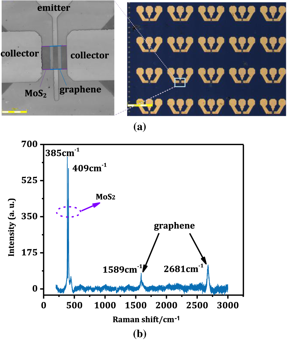
    Fig. 1. (a) Optical microscope image of the phototransistor device array and the grayscale image of a device. (b) Raman spectrum of the graphene/MoS2 heterojunction under excitation by a 532 nm laser.
    Production process of the Au/graphene/MoS2 vdWHs bipolar phototransistor.
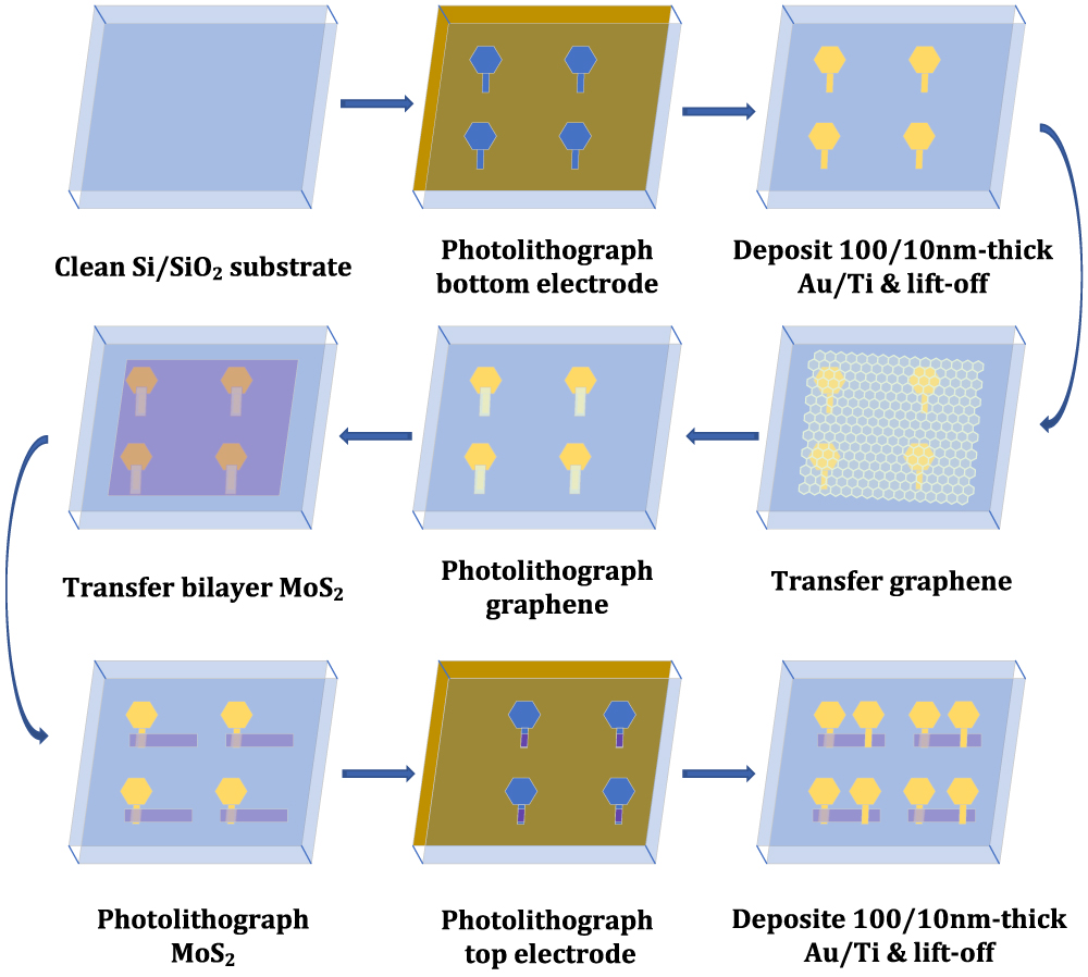
    Fig. 2. Production process of the Au/graphene/MoS2 vdWHs bipolar phototransistor.
    (a) I–V characteristic curve of Au-graphene junction. The Au is the cathode and the graphene layer is the anode. (b) I–V characteristic curve of graphene-MoS2 junction. The graphene is the cathode and the MoS2 is the anode. Band diagrams of the Au/graphene/MoS2 vdWHs (c) in their original state, (d) with forward bias and irradiation.
    Fig. 3. (a) IV characteristic curve of Au-graphene junction. The Au is the cathode and the graphene layer is the anode. (b) IV characteristic curve of graphene-MoS2 junction. The graphene is the cathode and the MoS2 is the anode. Band diagrams of the Au/graphene/MoS2 vdWHs (c) in their original state, (d) with forward bias and irradiation.
    (a) Schematic of the Au/graphene/MoS2 bipolar phototransistor and its equivalent structure. (b) I–V characteristics in darkness and under different irradiance intensity values (VG=0). (c) ICE versus laser power density under different VCE at VG=0 V. (d) VG versus ICE at different VCE with 1.05 mW/cm2 irradiance intensity. The wavelength of the laser is 405 nm.
    Fig. 4. (a) Schematic of the Au/graphene/MoS2 bipolar phototransistor and its equivalent structure. (b) IV characteristics in darkness and under different irradiance intensity values (VG=0). (c) ICE versus laser power density under different VCE at VG=0  V. (d) VG versus ICE at different VCE with 1.05  mW/cm2 irradiance intensity. The wavelength of the laser is 405 nm.
    (a) Responsivity of the device as a function of VCE under different VG. (b) Responsivity of the device as a function of laser power density at different VCE. (c) Relationship between photocurrent and dark current, normalized by the ratio Ilaser/Idark, and the detectivity of the bipolar phototransistor at different VCE values (irradiation under 405 nm 0.25 mW/cm2 irradiance intensity and VG=0 V). (d) Responsivity curves of Au/graphene/MoS2 vdWHs under different wavelengths of laser radiation with same laser power density 1.05 mW/cm2.
    Fig. 5. (a) Responsivity of the device as a function of VCE under different VG. (b) Responsivity of the device as a function of laser power density at different VCE. (c) Relationship between photocurrent and dark current, normalized by the ratio Ilaser/Idark, and the detectivity of the bipolar phototransistor at different VCE values (irradiation under 405 nm 0.25  mW/cm2 irradiance intensity and VG=0  V). (d) Responsivity curves of Au/graphene/MoS2 vdWHs under different wavelengths of laser radiation with same laser power density 1.05  mW/cm2.
    (a) Transient response of the Au/graphene/MoS2 bipolar phototransistor. (b) A section between 80 s and 90 s of (a) with a rise time of 20 ms and a fall time of 92 ms. (c) I–V characteristic curves of graphene/MoS2 vdWHs under irradiation. (d) The photocurrent density of the Au/graphene/MoS2 bipolar phototransistor and graphene/MoS2 photodiode under the same laser power density and the amplification coefficient β depends on the bias voltages. (Irradiation under 405 nm 0.45 mW/cm2 irradiance intensity, VCE=17 V and VG=0 V.)
    Fig. 6. (a) Transient response of the Au/graphene/MoS2 bipolar phototransistor. (b) A section between 80 s and 90 s of (a) with a rise time of 20 ms and a fall time of 92 ms. (c) IV characteristic curves of graphene/MoS2 vdWHs under irradiation. (d) The photocurrent density of the Au/graphene/MoS2 bipolar phototransistor and graphene/MoS2 photodiode under the same laser power density and the amplification coefficient β depends on the bias voltages. (Irradiation under 405 nm 0.45  mW/cm2 irradiance intensity, VCE=17  V and VG=0  V.)
    Summary of comparison of the responsivity performance and generation speed of photocurrent of our Au/graphene/MoS2 vdWH with other 2D heterostructures based on MoS2, showing that our device achieves the highest generation speed of photocurrent.
    Fig. 7. Summary of comparison of the responsivity performance and generation speed of photocurrent of our Au/graphene/MoS2 vdWH with other 2D heterostructures based on MoS2, showing that our device achieves the highest generation speed of photocurrent.
    Device MaterialsOperating WavelengthResponsivity (A/W)Detectivity (Jones)Ref.
    GaTe-MoS2473 nm21.838.4×1013[43]
    MoS2White2.5[31]
    WS2/MoS2532 nm23404.1×1011[22]
    MoS2&ALD532 nm1270[44]
    MoS2 homojunction635 nm70,0003.5×1014[45]
    Gr/MoS2/Gr532 nm10,000[46]
    Sb2Te3/MoS2532 nm3601×1012[20]
    Au/Gr/MoS2405 nm16,4581.75×1014This work
    Table 1. Summary of Comparison of the Au/graphene/MoS2 vdWHs with Other 2D Materials Heterostructures Based on Graphene or MoS2
    Jiaqi Li, Xurui Mao, Sheng Xie, Zhaoxin Geng, Hongda Chen. Bipolar phototransistor in a vertical Au/graphene/MoS2 van der Waals heterojunction with photocurrent enhancement[J]. Photonics Research, 2020, 8(1): 39
    Download Citation