
Wenyao Liang, Zheng Li, Yu Wang, Wuhe Chen, Zhiyuan Li, "All-angle optical switch based on the zero reflection effect of graphene–dielectric hyperbolic metamaterials," Photonics Res. 7, 318 (2019)
- Photonics Research
- Vol. 7, Issue 3, 318 (2019)
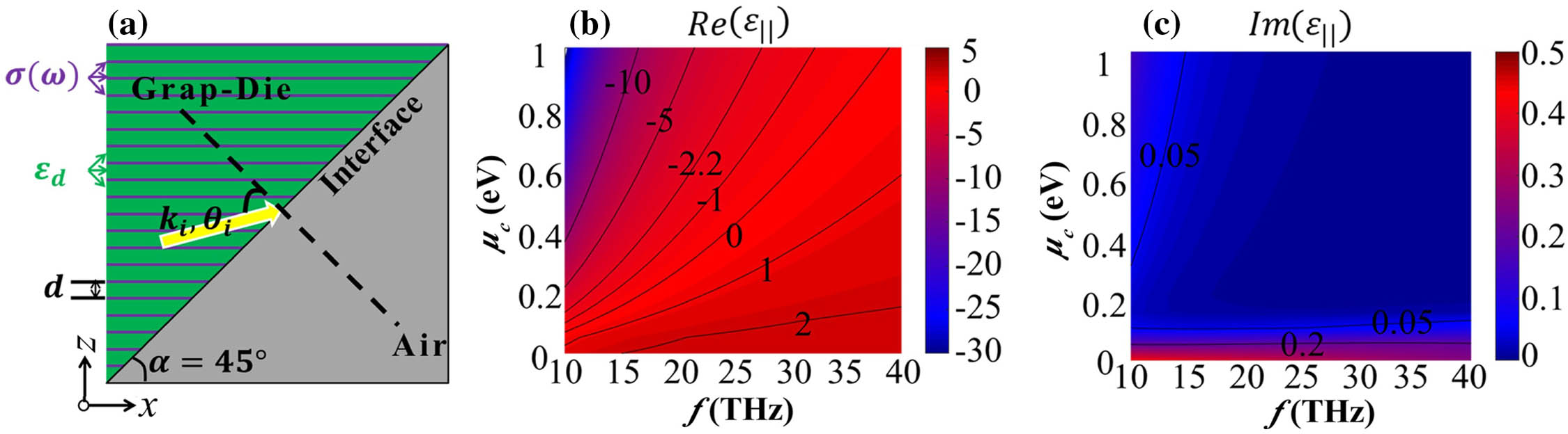
Fig. 1. (a) Schematic of the zero-reflection-based optical switch; the period of the SHM is d Re ( ε ‖ ) Im ( ε ‖ )
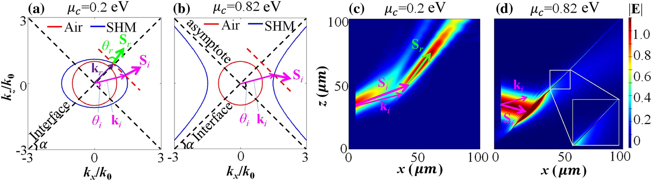
Fig. 2. IFC analysis and simulation results for the optical switch at θ i = 60 ° f = 25 THz μ c = 0.2 eV μ c = 0.82 eV
Fig. 3. Snapshots at different time steps for a Gaussian beam with a finite length of time steps. (a) t s = 100 t s = 200 t s = 2000
Fig. 4. Influence of absorption loss of dielectric layers on the optical switch. (a) OFF-state (μ c = 0.2 eV μ c = 0.82 eV
Fig. 5. Variation of reflection with chemical potential for f = 24.5 THz
Fig. 6. μ c - f ε ‖ = 0 d = 0.1 μm ε ‖ = − ε d d = 0.1 μm ε ‖ = 0 ε d = 1 ε ‖ = − 1 ε d = 1 μ c = 0.2 eV
Fig. 7. (a) μ c - f α = 20 ° f = 25 THz α = 80 ° ε ‖ = − 0.07 θ i max α


Set citation alerts for the article
Please enter your email address

© Copyright 2018-2021 | Chinese Laser Press. All Rights Reserved 沪ICP备15018463号-20