
Kin Fai Tse, Shengyuan Wang, Man Hoi Wong, Junyi Zhu. Defects properties and vacancy diffusion in Cu2MgSnS4[J]. Journal of Semiconductors, 2022, 43(2): 022101
- Journal of Semiconductors
- Vol. 43, Issue 2, 022101 (2022)
Abstract
1. Introduction
Kesterite Cu2ZnSnS4 (CZTS) is an earth-abundant, non-toxic absorber material for photovoltaics with a direct band gap tunable from 1.5 eV in pure CZTS[
Comparing CZTS to the Cu(In/Ga)S2 (CIGS) absorber material, CZTS often suffers from a high open-circuit voltage (VOC) deficit[
Despite the theoretical and experimental efforts in the development of processing techniques, an empirically lower EQE and VOC still persists in CZTSSe, contributing to the efficiency gap compared to record efficiency of higher than 20% in other thin film materials such as CIGS. It is suggested that intrinsic phase stability and electronic properties play an important role in the construction of high efficiency kesterite solar cells[
Cu2MgSnS4 (CMTS) is also a viable alternative that is less investigated in literature. Early work based on semi-local exchange-correlational functional predicts CMTS to have a small instability with respect to phase segregation into Cu2SnS4 and MgS[
CMTS is different from CZTS in that 1) a more ionic and larger covalent radius Mg replaces the role of Zn in CZTS; 2) the competing secondary phase MgS is of halite structure instead of the zinc-blende structure; and 3) the ground-state structure of CMTS is stannite, where Cu and Sn/Zn ions are organized into layers[
2. Electronic and thermodynamic properties
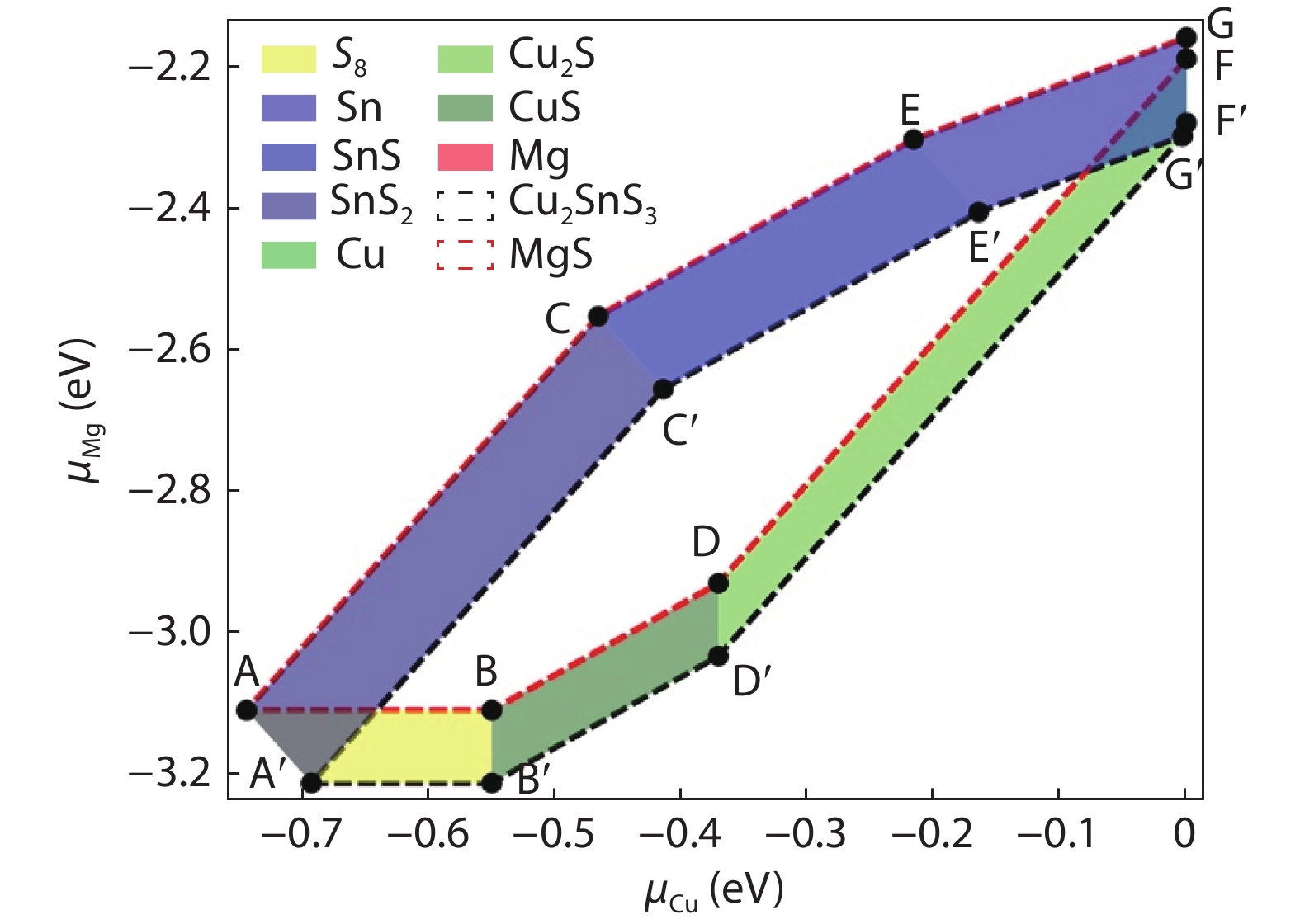
The phase diagram is calculated following the methodology of our earlier study for ease of discussion. The atomic chemical potential corresponding to the growth window of CMTS is calculated by requiring that, under the chemical potential window specified, CMTS is energetically stable while other secondary phases are unstable. Detailed thermodynamic discussions of CMTS are referred to in Ref. [42]. Formation energies for binary secondary phases including halite and zinc-blende MgS, and ternary secondary phases in CMTS as listed in other related works[
![]()
Figure 1.(Color online) Phase diagram of CMTS calculated from hybrid functional (HSE06).
We calculated a direct band gap of 1.61 eV for CMTS, showing a hybridization of Cu-3d (Sn-5s) and S-3p orbitals that are composed of the VB (CB). Meanwhile, Mg is not involved in the composition of VB or CB. Band alignment of CMTS with reference to CZTS is calculated through a CMTS(010)/CZTS(010) hetero-junction following the methodology of Himuma et al.[
3. Intrinsic defect formation
The formation of defect is governed by both the growth condition (atomic chemical potential) and the Fermi energy level, at equilibrium, the formation energy
where the third term sums over the energy required to remove
![]()
Figure 2.(Color online) Neutral defect formation energy for (a) intrinsic defects and (b) defect complexes in CMTS at chemical potentials ranging from Cu poorest (A) to Cu richest (G).
The local bonding environment of CMTS largely follows that of CZTS, in which one S atom is bonded directly to 2 Cu, 1 group II and 1 Sn atom, and each cation is bonded to 4 S atoms. We therefore expect that defect properties will be somewhat similar to CZTS. On the other hand, the difference in electronic structure and local stress can also enhance or suppress defect formation selectively where a larger size difference leads to an increase in defect formation energy[
Several defects including Cui, MgCu, SnMg and VS have lower formation energy in Cu rich limit (points E, F and G), while the formation energy of acceptor defects VCu and CuMg becomes higher. As a result, the Cu rich condition may lead to stronger charge compensation and higher concentration of donor defects that may deteriorate device performance. At chemical potential point B and D, neutral formation energy of all point defects except CuMg and VCu is above 1.6 eV. These chemical potentials correspond to a mildly Cu poor and Sn poor growth condition. As a comparison, the formation energy of a number of donor defects in CZTS are always between 1–1.5 eV at any chemical potential[
where
4. Defect complexes
Defect complexes can have significant influence on band edge positions[
The binding energy of defect complex can be negative because of the charge or stress compensation, and also Coulombic attraction between defects[
Literature in CZTS showed that Cu–Zn disorder is partly responsible to Voc loss, which may be explained by the low formation energy of Cu–Zn related defect complexes. In CMTS, we also show that fully compensated defect complexes CuMg+MgCu, (2Cu)Mg and Mg(2Cu) have a low formation energy less than 1 eV. The formation energy for CuMg+MgCu is 0.24 eV, similar to CuZn+ZnCu in CZTS. Because of the low formation energy, the concentration of CuMg+MgCu at equilibrium can be as high as >10 20 cm–3, which may not be desirable. Similarly to CZTS, these low energy defect complexes can possibly induce a Cu–Mg disorder phase in CMTS, and thus a careful control of growth temperature may also be required for the growth of CMTS.
Defect complexes involving Sn atom has a large binding energy due to stronger charge compensation between p- and n-type defects. In CZTS, ZnSn+SnZn can induce strong band gap shrinking, which can be a significant contributor to band gap fluctuation because of its low formation energy of 0.86 eV[
The formation energy of MgSn+SnMg in CMTS is higher by +0.49 eV, possibly lowering its concentration by several orders of magnitude. For other defect complexes involving Sn, the absolute formation energy of Sn related defect complexes is not lowered significantly past that of an isolated point defect, together with the large binding energy. Such a mechanism may also help convert deep intrinsic defects into defect complexes that are less electrically active.
5. Electronic properties of defects
In this part, we examine the dependence of charge transition level on the Fermi energy level. The charged defect formation energy at chemical potential point B is shown in Fig. 3. In CMTS, CuMg shows properties analogous to CuZn in CZTS. CuMg can be ionized to –1 charge state, the ionized state is energetically more favorable when Fermi energy level is higher than VBM + 0.21 eV, slightly deeper than CuZn in CZTS[
![]()
Figure 3.(Color online) Charged defect formation energy of point defects at chemical potential B, Fermi energy is varied from VBM to CBM.
Our calculations show that anion defects in CMTS do not show charge transition within the band gap. Acceptor defects MgSn and CuSn can have multiple transitions into lower energy negatively charged states as the Fermi energy level moves towards CBM. Around the pinned Fermi energy level, these defects remain charge neutral and has a high formation energy above 2 eV. However, we find that the SnMg defect has a deep (0/2+) charge transition at VBM + 0.55 eV near the mid gap with relatively low formation energy of 1.77 eV in a neutral state at chemical potential point B, which can serve as carrier traps. Such a negative-U center is more detrimental than SnZn in CZTS because of relatively low formation energy[
We then explore the scenario where defect concentration is high. At high defect concentration, defect bands may be formed leading to band tailing, which is commonly regarded as a major contribution to loss of open circuit voltage in CZTS[
6. Vacancy-mediated diffusion
Lastly, we show our results regarding the diffusion kinetics of a few point defects in CMTS. Defect thermodynamics provide a good estimation of bulk defect density when spatial variation of atom stoichiometry can be minimized, that is, when the diffusion is relatively quick, it is thus important also to understand the diffusion kinetics in CMTS. As we have already showed that the formation energy of Cu and S vacancies are relatively low in CMTS, the density of these defects should be relatively high, thus our current result focuses on the diffusion of atoms in the presence of Cu or S vacancy. Moreover, the activation energy of diffusions through VCu is found to be relatively low in both CZTS and CIGS. Therefore, our result on CMTS can provide qualitative insight into the diffusion properties of CMTS. The chosen diffusion paths are shown in Fig. 4. Diffusion simulation is conducted via the nudged elastic band method with a climbing image using seven images between optimized initial and final defect configurations to provide smooth interpolation to the reaction energetics and good estimation of activation energy[
![]()
Figure 4.(Color online) Illustration of vacancy diffusion paths investigated in the current study.
Relative energy along minimum energy path (MEP) is shown in Fig. 5. The activation energy for the diffusion of VCu is 1.23 eV in CMTS, which is similar to Cu diffusion via vacancies in CZTS and CIGS system. For Mg diffusion into VCu, the formation energy is 0.18 eV lower (1.05 eV). In comparison, Zn diffusion into VCu in CZTS is 0.13 eV higher than diffusion of copper vacancy, indicating that Mg is also a relatively mobile atom species in CMTS. On the other hand, Sn diffusion into VCu has a much higher activation energy. This is partly due to the higher formation energy of Sn defect and relatively large atomic size of Sn. This high diffusion barrier may also help to prevent the formation of Sn antisite defect, which we considered detrimental in CMTS. VS represents the vacancy-mediated diffusion of S atom in CMTS with all initial and final configuration of VS being equivalent, thus the energy profile along the MEP should be symmetric. Despite this, we have not enforced such symmetry during the calculation, and our result shows an almost symmetric energy profile, indicating that the images are well-converged to minimal energy. For all S vacancy diffusion in CMTS, the activation energy is at the minimal 1.86 eV with a strong asymmetry. When S atoms diffuse across Sn atoms, additional energy is required to lose the stronger S–Sn bonding, which results in the diffusion barrier of S across the Cu layer to be significantly lower. Our result shows calculated activation energy for Sn and S diffusion has an activation energy comparable to In diffusion in CISe[
![]()
Figure 5.(Color online) Energy relative to VCu for cation and VS for anion diffusion along the MEP, energies of calculated images are represented by markers and solid lines are interpolation.
7. Conclusion
We presented a systematic study of point defects and a few defect complexes in CMTS using the HSE06 functional within the density functional theory framework. Our calculation shows that the growth window of CMTS is similar to that of CZTS, and there is an increase in formation energy for most defects compared to CZTS hence a lower defect density. Such an elevation reduces the concentration of MgSn and CuSn defects with multiple charge states. Then we predict a p-type behavior due to ionization of CuMg to CuMg–, showing the Fermi energy located around 0.2 eV above the valence band due to compensation with a MgCu defect. However, we still unearth a strong Cu/Mg compositional fluctuation due to low formation energy for a CuMg+MgCu defect complex, analogous to CZTS results. And we identify SnMg double donor defect as the likely detrimental defect in CMTS system because of high density at Sn-rich or Cu-rich chemical potential, and a deep donor level in the mid gap. The profile of the SnMg defect is inferior than SnZn in CZTS. To avoid a high concentration of the SnMg defect, we propose tuning the chemical potential to Sn-poor and Cu mildly poor condition or anneal at lower temperature. Finally, we justify our defect finding with a comparison of activation energy of vacancy diffusion in CMTS and CZTS. We find the Cu and Mg diffusion through VCu to be relatively quick, and the activation energy of these diffusion mechanisms are similar to previous reported values in CZTS and CIGS.
Acknowledgements
The authors would like to acknowledge support from Research Grants Council of Hong Kong (under GRF/14319416, GRF/14301318, and Direct Grant).
References
[1] S Y Chen, X G Gong, A Walsh et al. Crystal and electronic band structure of Cu2ZnSnX4 (X = S and Se) photovoltaic absorbers: First-principles insights. Appl Phys Lett, 94, 041903(2009).
[2] J He, L Sun, S Y Chen et al. Composition dependence of structure and optical properties of Cu2ZnSn(S, Se)4 solid solutions: An experimental study. J Alloys Compd, 511, 129(2012).
[3] S Levcenco, D Dumcenco, Y P Wang et al. Influence of anionic substitution on the electrolyte electroreflectance study of band edge transitions in single crystal Cu2ZnSn(S
[4] C Persson. Electronic and optical properties of Cu2ZnSnS4 and Cu2ZnSnSe4. J Appl Phys, 107, 053710(2010).
[5] W Wang, M T Winkler, O Gunawan et al. Device characteristics of CZTSSe thin-film solar cells with 12.6% efficiency. Adv Energy Mater, 4, 1301465(2014).
[6] C Yan, J L Huang, K W Sun et al. Cu2ZnSnS4 solar cells with over 10% power conversion efficiency enabled by heterojunction heat treatment. Nat Energy, 3, 764(2018).
[7] X L Liu, Y Feng, H T Cui et al. The current status and future prospects of kesterite solar cells: A brief review. Prog Photovolt: Res Appl, 24, 879(2016).
[8] D M Bishop, B McCandless, T Gershon et al. Modification of defects and potential fluctuations in slow-cooled and quenched Cu2ZnSnSe4 single crystals. J Appl Phys, 121, 065704(2017).
[9] S Zhuk, A Kushwaha, T K S Wong et al. Critical review on sputter-deposited Cu2ZnSnS4 (CZTS) based thin film photovoltaic technology focusing on device architecture and absorber quality on the solar cells performance. Sol Energy Mater Sol Cells, 171, 239(2017).
[10] O Gunawan, T K Todorov, D B Mitzi. Loss mechanisms in hydrazine-processed Cu2ZnSn(Se, S)4 solar cells. Appl Phys Lett, 97, 233506(2010).
[11] D Han, Y Y Sun, J Bang et al. Deep electron traps and origin of p-type conductivity in the earth-abundant solar-cell material Cu2ZnSnS4. Phys Rev B, 87, 155206(2013).
[12] S Y Chen, A Walsh, X G Gong et al. Classification of lattice defects in the kesterite Cu2ZnSnS4 and Cu2ZnSnSe4 earth-abundant solar cell absorbers. Adv Mater, 25, 1522(2013).
[13] T Gokmen, O Gunawan, T K Todorov et al. Band tailing and efficiency limitation in kesterite solar cells. Appl Phys Lett, 103, 103506(2013).
[14] M J Romero, H Du, G Teeter et al. Comparative study of the luminescence and intrinsic point defects in the kesterite Cu2ZnSnS4 and chalcopyrite Cu(In, Ga)Se2thin films used in photovoltaic applications. Phys Rev B, 84, 165324(2011).
[15] G Rey, G Larramona, S Bourdais et al. On the origin of band-tails in kesterite. Sol Energy Mater Sol Cells, 179, 142(2018).
[16] J J Li, D X Wang, X L Li et al. Cation substitution in earth-abundant kesterite photovoltaic materials. Adv Sci, 5, 1700744(2018).
[17] K Pal, P Singh, A Bhaduri et al. Current challenges and future prospects for a highly efficient (>20%) kesterite CZTS solar cell: A review. Sol Energy Mater Sol Cells, 196, 138(2019).
[18] A Kanevce, I Repins, S H Wei. Impact of bulk properties and local secondary phases on the Cu2(Zn, Sn)Se4 solar cells open-circuit voltage. Sol Energy Mater Sol Cells, 133, 119(2015).
[19] V Kosyak, A V Postnikov, J Scragg et al. Calculation of point defect concentration in Cu2ZnSnS4: Insights into the high-temperature equilibrium and quenching. J Appl Phys, 122, 035707(2017).
[20] D Huang, C Persson. Band gap change induced by defect complexes in Cu2ZnSnS4. Thin Solid Films, 535, 265(2013).
[21] P Zawadzki, A Zakutayev, S Lany. Entropy-driven clustering in tetrahedrally bonded multinary materials. Phys Rev Appl, 3, 034007(2015).
[22] J J S Scragg, L Choubrac, A Lafond et al. A low-temperature order-disorder transition in Cu2ZnSnS4 thin films. Appl Phys Lett, 104, 041911(2014).
[23] B G Mendis, M C J Goodman, J D Major et al. The role of secondary phase precipitation on grain boundary electrical activity in Cu2ZnSnS4 (CZTS) photovoltaic absorber layer material. J Appl Phys, 112, 124508(2012).
[24] W C Yang, C K Miskin, N J Carter et al. Compositional inhomogeneity of multinary semiconductor nanoparticles: A case study of Cu2ZnSnS4. Chem Mater, 26, 6955(2014).
[25] J J Scragg, J T Wätjen, M Edoff et al. A detrimental reaction at the molybdenum back contact in Cu2ZnSn(S, Se)4 thin-film solar cells. J Am Chem Soc, 134, 19330(2012).
[26] J J Scragg, T Kubart, J T Wätjen et al. Effects of back contact instability on Cu2ZnSnS4 devices and processes. Chem Mater, 25, 3162(2013).
[27] G K Dalapati, S Zhuk, S Masudy-Panah et al. Impact of molybdenum out diffusion and interface quality on the performance of sputter grown CZTS based solar cells. Sci Rep, 7, 1350(2017).
[28] M Bär, B A Schubert, B Marsen et al. Cliff-like conduction band offset and KCN-induced recombination barrier enhancement at the CdS/Cu2ZnSnS4 thin-film solar cell heterojunction. Appl Phys Lett, 99, 222105(2011).
[29] A Nagaoka, H Miyake, T Taniyama et al. Effects of sodium on electrical properties in Cu2ZnSnS4 single crystal. Appl Phys Lett, 104, 152101(2014).
[30] T Gershon, B Shin, N Bojarczuk et al. The role of sodium as a surfactant and suppressor of non-radiative recombination at internal surfaces in Cu2ZnSnS4. Adv Energy Mater, 5, 1400849(2015).
[31] Y O Zhang, K Tse, X D Xiao et al. Controlling defects and secondary phases of CZTS by surfactant potassium. Phys Rev Mater, 1, 045403(2017).
[32] C Yan, F Y Liu, N Song et al. Band alignments of different buffer layers (CdS, Zn(O, S), and In2S3) on Cu2ZnSnS4. Appl Phys Lett, 104, 173901(2014).
[33] K W Sun, C Yan, F Y Liu et al. Over 9% efficient kesterite Cu2ZnSnS4 solar cell fabricated by using Zn1–
[34] X L Li, Z H Su, S Venkataraj et al. 8.6% Efficiency CZTSSe solar cell with atomic layer deposited Zn-Sn-O buffer layer. Sol Energy Mater Sol Cells, 157, 101(2016).
[35] J J Li, X R Liu, W Liu et al. Restraining the band fluctuation of CBD-Zn(O, S) layer: Modifying the hetero-junction interface for high performance Cu2ZnSnSe4 solar cells with Cd-free buffer layer. Sol RRL, 1, 1700075(2017).
[36] H T Cui, X L Liu, F Y Liu et al. Boosting Cu2ZnSnS4 solar cells efficiency by a thin Ag intermediate layer between absorber and back contact. Appl Phys Lett, 104, 041115(2014).
[37] F Y Liu, K W Sun, W Li et al. Enhancing the Cu2ZnSnS4 solar cell efficiency by back contact modification: Inserting a thin TiB2 intermediate layer at Cu2ZnSnS4/Mo interface. Appl Phys Lett, 104, 051105(2014).
[38] X L Liu, H T Cui, W Li et al. Improving Cu2ZnSnS4 (CZTS) solar cell performance by an ultrathin ZnO intermediate layer between CZTS absorber and Mo back contact. Phys Status Solidi RRL, 8, 966(2014).
[39] Z F Tong, K Zhang, K W Sun et al. Modification of absorber quality and Mo-back contact by a thin Bi intermediate layer for kesterite Cu2ZnSnS4 solar cells. Sol Energy Mater Sol Cells, 144, 537(2016).
[40] Y C Gu, H P Shen, C Ye et al. All-solution-processed Cu2ZnSnS4 solar cells with self-depleted Na2S back contact modification layer. Adv Funct Mater, 28, 1703369(2018).
[41] C C Wang, S Y Chen, J H Yang et al. Design of I2–II–IV–VI4 semiconductors through element substitution: The thermodynamic stability limit and chemical trend. Chem Mater, 26, 3411(2014).
[42] G H Zhong, K Tse, Y O Zhang et al. Induced effects by the substitution of Zn in Cu2ZnSnX4 (X = S and Se). Thin Solid Films, 603, 224(2016).
[43] Z K Yuan, S Y Chen, H J Xiang et al. Engineering solar cell absorbers by exploring the band alignment and defect disparity: The case of Cu- and Ag-based kesterite compounds. Adv Funct Mater, 25, 6733(2015).
[44] Y F Qi, D X Kou, W H Zhou et al. Engineering of interface band bending and defects elimination via a Ag-graded active layer for efficient (Cu, Ag)2ZnSn(S, Se)4 solar cells. Energy Environ Sci, 10, 2401(2017).
[45] Z H Su, J M R Tan, X L Li et al. Cation substitution of solution-processed Cu2ZnSnS4 thin film solar cell with over 9% efficiency. Adv Energy Mater, 5, 1500682(2015).
[46] S Bag, O Gunawan, T Gokmen et al. Hydrazine-processed Ge-substituted CZTSe solar cells. Chem Mater, 24, 4588(2012).
[47] A D Collord, H W Hillhouse. Germanium alloyed kesterite solar cells with low voltage deficits. Chem Mater, 28, 2067(2016).
[48] M Wei, Q Y Du, R Wang et al. Synthesis of new earth-abundant kesterite Cu2MgSnS4 nanoparticles by hot-injection method. Chem Lett, 43, 1149(2014).
[49] G L Agawane, S A Vanalakar, A S Kamble et al. Fabrication of Cu2(Zn
[50] G Yang, X L Zhai, Y F Li et al. Synthesis and characterizations of Cu2MgSnS4 thin films with different sulfuration temperatures. Mater Lett, 242, 58(2019).
[51] R Caballero, S G Haass, C Andres et al. Effect of magnesium incorporation on solution-processed kesterite solar cells. Front Chem, 6, 5(2018).
[52] S Lie, S W Leow, D M Bishop et al. Improving carrier-transport properties of CZTS by Mg incorporation with spray pyrolysis. ACS Appl Mater Interfaces, 11, 25824(2019).
[53] S Y Chen, J H Yang, X G Gong et al. Intrinsic point defects and complexes in the quaternary kesterite semiconductor Cu2ZnSnS4. Phys Rev B, 81, 245204(2010).
[54] Y Hinuma, A Grüneis, G Kresse et al. Band alignment of semiconductors from density-functional theory and many-body perturbation theory. Phys Rev B, 90, 155405(2014).
[55] S H Wei. Overcoming the doping bottleneck in semiconductors. Comput Mater Sci, 30, 337(2004).
[56] C Freysoldt, J Neugebauer, C G van de Walle. Fully ab initio finite-size corrections for charged-defect supercell calculations. Phys Rev Lett, 102, 016402(2009).
[57] S Y Chen, X G Gong, A Walsh et al. Electronic structure and stability of quaternary chalcogenide semiconductors derived from cation cross-substitution of II-VI and I-III-VI2 compounds. Phys Rev B, 79, 165211(2009).
[58] J Y Zhu, F Liu, G B Stringfellow et al. Strain-enhanced doping in semiconductors: Effects of dopant size and charge state. Phys Rev Lett, 105, 195503(2010).
[59] H Hu, M Liu, Z F Wang et al. Quantum electronic stress: Density-functional-theory formulation and physical manifestation. Phys Rev Lett, 109, 055501(2012).
[60] R Noufi, R Axton, C Herrington et al. Electronic properties versus composition of thin films of CuInSe2. Appl Phys Lett, 45, 668(1984).
[61] W Xiao, J N Wang, X S Zhao et al. Intrinsic defects and Na doping in Cu2ZnSnS4: A density-functional theory study. Sol Energy, 116, 125(2015).
[62] G Henkelman, B P Uberuaga, H Jónsson. A climbing image nudged elastic band method for finding saddle points and minimum energy paths. J Chem Phys, 113, 9901(2000).
[63] J P Perdew, K Burke, M Ernzerhof. Generalized gradient approximation made simple. Phys Rev Lett, 77, 3865(1996).
[64] S Nakamura, T Maeda, T Wada. First-principles study of diffusion of Cu and in atoms in CuInSe2. Jpn J Appl Phys, 52, 04CR01(2013).

Set citation alerts for the article
Please enter your email address
© Copyright 2018-2021 | Chinese Laser Press. All Rights Reserved 沪ICP备15018463号-20