Author Affiliations
1State Key Laboratory of Infrared Physics, Shanghai Institute of Technical Physics, Chinese Academy of Sciences, Shanghai 200083, China2Hangzhou Institute for Advanced Study, University of Chinese Academy of Sciences, Hangzhou 310024, China3College of Materials Science and Engineering, Zhengzhou University, Zhengzhou 450052, China4University of Chinese Academy of Sciences, Beijing 100049, Chinashow less
Abstract
The hetero-interface induced anomalous photoluminescence (PL) emissions in the vertical WS2/Ga2O3 heterostructures was demonstrated. The WS2/Ga2O3 hetero-interface varies type-II band structure and brings subsequent PL decline in the bottom WS2 monolayer contacted with Ga2O3 layer. Such hetero-interlayer coupling interaction between oxides and 2D layered transition metal dichalcogenides (TMDs) in the stacked heterostructures impacts interlayer interaction between the bottom WS2 monolayer and the upper WS2 monolayer in a WS2 bilayer, which leads to an anomalous PL enhancement in the bilayer WS2. Stacked hetero-interface will benefit for controlling the optical or electronic behavior and modulating energy band structures by customizing transformative 2D heterostructures used in next-generation nanoscale optoelectronic detectors and photodetectors.Introduction
Stacked van der Waals heterostructures have extended versatile electrical,optical and chemical properties of individual 2D materials,and recently drawn broad attentions in optoelectronic detection and photodetection fields[1-9]. The interfaces and interlayer interactions have shown significant impact on the energy band structure,charge transfer and density distribution,and defect formation in 2D heterostructures[3-4,10-14]. While the underlying physical mechanism still needs be further explored,2D vertical heterostructures and interfacial engineering have become a promising platform to artificially design and manipulate desired atomic layered heterostructures and photodetectors. Notably,2D TMDs(e.g.,MoS2,WS2)can emit pronounced photoluminescence(PL)by exciton recombination and release photons at room temperature[11,15]. Monolayer WS2 possesses a direct band gap and abundant exciton behaviors for high PL quantum yield owing to strong light-matter coupling and thin dielectric screening in an atomic monolayer. However,the non-conservation of electron momentum will lead to a poor PL in a bilayer WS2[16-17]. The PL behaviors in 2D TMDs are determined by the energy band structure and exciton energy related to interlayer interaction,defects or doping. For a 2D interlayer stacking,the defect energy levels and bound excitons will also change energy band structure,transition behaviors of electrons and photons,and the proportion of excitons in TMDs[18-20].
In van der Waals heterostructure,the interfacial interaction is ubiquitous and vital to significantly modulate and alter the optical and optoelectronic properties of 2D materials[6,21]. Hetero-interface strategies have provided a great opportunity to design and construct 2D stacked heterojunctions by band alignment engineering for the advanced microelectronic and optoelectronic detection devices[9,22]. It still remains challenging great to control complex and versatile interfaces in 2D homostructures and heterostructures. Various interface-engineering methods have been exploited to manipulate 2D heterostructures and their functions. Both CVD(i.e., chemical vapor deposition)growth and mechanical transferring/stacking have been exploited to design and realize 2D van der Waals heterostructures on the desired substrates. Especially,during a CVD process,clean surface and original interface coupling can be feasibly obtained in 2D heterostructures[10,23-24]. Emerging 2D hetero-interfaces between TMDs and traditional semiconductors have sparked intensive interest in 2D heterostructures. Various Ga2O3 materials have been exploited to fabricate deep-ultraviolet photodetectors,functional FETs and high-power devices[25-27]. Excellent electronic-photonic properties and high temperature-stability of Ga2O3 makes it possible to design and directly fabricate TMDs/oxide heterostructures.
In this work,we demonstrate an anomalous PL in the bilayer WS2 induced by a hetero-interface between WS2 layers and Ga2O3 thin films. In virtue of CVD-grown WS2/Ga2O3 heterostructures on SiO2/Si substrates,we analyzed surface-dependent PL and the role of interfaces. Converse PL was found and anomalous in the region of bilayer-WS2 on the Ga2O3 thin films. The PL intensity in the bilayer WS2(i.e., 2L-WS2)region is approximately 10 times stronger than that in the monolayer WS2(i.e., 1L-WS2)region. Such anomalous PL behaviors in bilayer WS2 depend on hetero-interface and modified energy band structures in the WS2/Ga2O3 heterostructure. WS2/oxide hetero-interfaces provide an alternative route to understand and manipulate the optical and electronic behaviors of 2D vertical heterostructures and functional detection devices.
1 Materials and methods
The 2D WS2/Ga2O3 vertical heterostructures are directly fabricated by a CVD method. In brief,the Ga2O3 thin films were atomic-layer-deposited on the SiO2/Si substrates as we reported elsewhere[26-27]. The layered WS2 was subsequently CVD-grown on the as-prepared Ga2O3 thin film,which may help for a clean hetero-interface in WS2/Ga2O3 vertical heterostructure. Thus,WO3 and S powders were used as precursors during the CVD-growth of 2D WS2 and WS2/Ga2O3 heterostructures grown at ~850 °C. High-resolution Raman/PL maps were obtained with 100 × objective,1 800/300 G/mm grating,and a scanning step of 300 nm while the intensity of 532 nm laser is less than 1 mW. Raman/PL spectroscopy was performed at room temperature. To fabricate transferred-WS2/Ga2O3 heterostructure,the target WS2 flakes on the SiO2/Si substrate were pasted on a cut polyvinyl alcohol hydrogel sheet,and then transferred onto the Ga2O3 thin film on SiO2/Si substrate according to the processes reported elsewhere. Briefly,KPFM image was obtained on Veeco/DI multimode SPM while optical microscopy was performed on Leica DM4000M[28-29].
2 Results and discussions
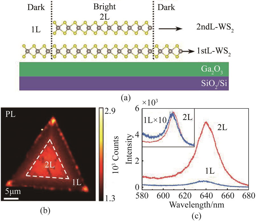
Figure 1(a)displays a schematic illustration of the 2D WS2/Ga2O3 vertical heterostructure on SiO2/Si substrates. Here,the bottom monolayer in bilayer-WS2 contacted Ga2O3 thin film was referred as first layer WS2(i.e.,1stL-WS2)while the upper layer as second layer WS2(i.e., 2ndL-WS2). Generally,the PL intensity of the 1stL-WS2 is much stronger than that of the 2ndL-WS2 in the bilayer-WS2 obtained on SiO2/Si substrates[16]. Nonetheless,an entire converse PL phenomenon was found from PL intensity map(at 640 nm)of the bilayer-WS2/Ga2O3 heterostructure,as shown in Fig. 1(b). The PL intensity in the 2L-WS2 domain surrounded by the white dashed triangle is evidently much stronger than that in the 1L-WS2 domain. Figure 1(c)shows obvious contrast PL spectra in the 1L-WS2 and 2L-WS2 domains. The inset reveals that the PL intensity in the 2L-WS2 domain is approximately 10 times stronger than the intensity in the 1L-WS2 domain. Notably,the anomalous PL emissions were observed in at least six cases of CVD-grown WS2/Ga2O3 heterostructures,where the stronger PL intensity of 2L-WS2 is than that of 1L-WS2. Subsequently,we further focused on such anomalous PL enhancement and the roles of the hetero-interface between Ga2O3 and the 1stL-WS2,and the homo-interface between the 1stL-WS2 and the 2ndL-WS2 in the bilayer-WS2/Ga2O3 heterostructure.

Figure 1.(a)Structural model schematic illustration of bilayer-WS2/Ga2O3 heterostructure,(b)PL intensity map(at a wavelength of 640 nm)of layered WS2 on Ga2O3 thin film,(c)PL spectra of the 1 L-WS2 and 2 L-WS2 domains in the heterostructure shown in(b)
Interlayer interactions and interfaces affect and even determine PL emission of 2D materials[17,30]. Therefore,we thought that the hetero-interlayer coupling between the bottom Ga2O3-layer and the 1stL-WS2 layer might play an important role in the anomalous PL. The PL emission intensity of 1L-WS2 decreases as displayed in Fig. 1(c),which might relate with the energy band structure and changed crystal lattice of the 1stL-WS2[31]. The WS2/Ga2O3 hetero-interface should be different from those in the WS2/SiO2 and 1stL/2ndL WS2 cases due to some possible changes in dielectric interfaces and interlayer spacing[32]. Such WS2/Ga2O3 hetero-interface might change the homo-interlayer coupling between the 1stL-WS2 and the 2ndL-WS2,which leads to a special 1L-WS2 and 2L-WS2 different from that in the cases of monolayer WS2 and bilayer-WS2 on the SiO2/Si substrates. As a consequence,all of these may lead to a stronger PL emission in the 2L-WS2 region while a weaker one in the 1L-WS2.
Figure 2 further shows optical image and Raman measurements of the 1st-layer and the 2nd-layer WS2 region in the bilayer WS2/Ga2O3 heterostructure. As represented in Fig. 2(a),1L-WS2 and 2L-WS2 domains are easily distinguished from the optical contrast. In Raman spectra,the in-plane shear vibration(2LA and)and the out-plane layer breathing vibration()locate at ~350 cm-1 and ~420 cm-1,respectively[33]. In addition,for the vibration peak at ~350 cm-1,the second-order 2LA mode is dominant due to the double-resonance process[34]. Moreover,varying with layer number,the intensity of mode(Fig. 2(b))is effectively discriminated in the Raman map in Fig. 2(b). The peak intensity of 2L-WS2 (pink region)is stronger than that of 1L-WS2(blue region). The ratio of the intensities of two characteristic peaks(i.e.,)is calculated and approximately 4.38 for the 1L-WS2 while that is about 2.82 for the 2L-WS2 (Fig. 2(c)). The value of decreased as the layer number increased,and then was exploited to further check and distinguish 1L-WS2 and 2L-layer WS2 as reported elsewhere[35].
Figure 2.(a)Optical microscopy image of bilayer WS2/Ga2O3 heterostructure,(b)corresponding Raman mode intensity map of bilayer-WS2 on Ga2O3 thin film in(a),the blue region is the 1 L region marked in(a)while the 2 L region is shown as the red,(c)Raman spectra of 1L-WS2 and 2L-WS2 in the heterostructure
For further comparison,a trilayer-WS2/Ga2O3 heterostructure were checked and investigated as suggested in Fig. 3. Optical contrast in Fig. 3(a)changes and is different in the 1L,2L,and 3L-WS2 domains. Raman intensity map in Fig. 3(c)also displays and manifests the corresponding 1L-WS2(blue region),2L-WS2(pink region)and 3L-WS2(white region)domains. As mentioned above,the intensity of vibration increases with layer number. The value of decreases with the increase of layer number,and is approximately 4.93,2.94,and 2.58 for 1L-WS2,2L-WS2 and 3L-WS2,respectively. Typically,the value of is more than 5 for a WS2 monolayer on SiO2/Si substrate,but it is less than 5 for that of 1L-WS2 in WS2/Ga2O3 heterostructure,which implies that the vibration mode of 1L-WS2 may be changed by the hetero-interface between Ga2O3 and 1stL-WS2[35].
Figure 3.(a)Optical image of trilayer-WS2/Ga2O3 heterostructure,(b)PL intensity map of WS2 on Ga2O3 thin film,(c)Raman mode intensity map of WS2 on Ga2O3 thin film,(d)PL and(e)Raman spectra of 1 L-WS2,2 L-WS2 and 3 L-WS2 in the heterostructure shown in(a)
Furthermore,the PL intensity of trilayer-WS2 on Ga2O3 reveals the dark-bright-dark alternating arrangement from accordant outer-1L to inner-3L as indicated in the PL intensity map in Fig. 3(b). The respective PL spectra are extracted from PL intensity map,as shown in Fig. 3(d). We noted that the PL intensity of 2L-WS2 is higher than that of 3L-WS2 while the one of 1L-WS2 is the lowest. Moreover,a redshift of ~5 nm in the PL between 1L-WS2 and 2L-WS2 is shown in Fig. 3(d),and but such shifts do not occur in the case of trilayer-WS2 on the SiO2/Si substrate. All these convincingly suggest that the hetero-interface between 1stL-WS2 and underlying Ga2O3 thin film plays a critical role in changing and weakening PL of 1L-WS2. The hetero-interface between the bottom 1stL-WS2 and the underlying Ga2O3 thin film might reduce the homo-interlayer coupling between 1stL-WS2 and 2ndL-WS2.
Monolayer-WS2/Ga2O3 heterostructure in Fig. 4 is used to further check and certify the role of hetero-interface. The optical contrast of OM image(Fig. 4(a))and intensity consistency of PL/Raman maps(Fig. 4(b)and 4(c))display and confirm the monolayer-WS2/Ga2O3 heterostructure. Figure 4(e)implies that the value of the WS2 monolayer in monolayer-WS2/Ga2O3 heterostructure is approximately 4.00 from Raman spectra,which also results from the WS2/Ga2O3 interface interaction as mentioned above. In addition,the PL intensity of monolayer-WS2 in the heterostructure in Fig. 4(d)is less than that of monolayer-WS2 on the SiO2/Si substrate. Notably,the PL intensity of 1L-WS2 in bilayer-WS2/Ga2O3 heterostructure(Fig. 1c)is less than that of the WS2 monolayer(Fig. 4(d)). In addition,the PL intensity of 2L-WS2 is stronger than both the one of 1L-WS2 in bilayer-WS2/Ga2O3 heterostructure(Fig. 1c)and that of the WS2 monolayer(Fig. 4(d)). All these results reveal that the presence of 2L-WS2 in bilayer-WS2/Ga2O3 heterostructure may further weaken the PL intensity of the 1L-WS2 in bilayer-WS2/Ga2O3 heterostructure. The varied energy band structure and possible interlayer charge transfer in both 1L-WS2 and 2L-WS2 may play an important role in an increasing PL intensity of 2L-WS2 and a weaken PL intensity in the bilayer-WS2/Ga2O3 heterostructure.
Figure 4.(a)Optical image of monolayer-WS2/Ga2O3 heterostructure,(b)PL intensity map of WS2 on Ga2O3 thin film,(c)Raman mode intensity map of WS2 on Ga2O3 thin film,(d)PL spectrum and(e)Raman spectrum of WS2 in monolayer WS2/Ga2O3 heterostructure
It has been documented that different contacted materials means different interfaces and dielectric environments[13,36-38]. Figure 5 shows the PL variation in the trilayer-WS2 on SiO2/Si substrate,and further verifies the roles of different interfaces on the PL intensity distribution of layered WS2. Figure 5(a)displays the different layer-domains distribution and the optical contrast in the trilayer-WS2 on SiO2/Si substrate. As illustrated in Fig. 5(b),the 1L-WS2 on SiO2/Si substrate displays the strongest PL emission,which is far outweighing that of 2L-WS2 and 3L-WS2. Thus,it is hard to distinguish the 2L and 3L-WS2 domains in Fig. 5(b). Figure 5(c)shows the Raman map of trilayer-WS2 on the SiO2/Si substrate and the different layer-domains marked by dashed triangles.
Figure 5.(a)Optical image of trilayer-WS2 on the SiO2/Si substrate,(b)PL intensity map of WS2 on the SiO2/Si substrate,(c)Raman mode intensity map of WS2 on the SiO2/Si substrate,(d)PL and(e)Raman spectra of 1L-WS2,2L-WS2 and 3L-WS2 shown in(a)
PL spectra of each layer in the trilayer-WS2 on SiO2/Si substrate are taken from Fig. 5(b)and then represented in Fig. 5(d). The PL intensity in 1L region is much larger than that in 2L and 3L regions because the PL intensity of WS2 decreases sharply with the increase of the layer number. Monolayer WS2 possesses direct band gap while bilayer and few layers WS2 are generally indirect band gap. Notably,the PL peak position of each layer in the trilayer-WS2 on SiO2/Si substrate is near 630 nm. Figure 5(e)shows the values of for 1L-WS2,2L-WS2 and 3L-WS2 is approximately 6.59,4.52,1.74,respectively. Here,the value of the 1L-WS2 in the trilayer-WS2 on SiO2/Si substrate is larger than 5. All these are different from those in the case of the trilayer-WS2/Ga2O3 heterostructure above,and further suggest that the hetero-interface between Ga2O3 thin film and WS2 definitely affects the optical band gap of WS2.
To further prove and understand the role of WS2/Ga2O3 hetero-interfaces on PL emission of WS2,we also constructed transferred-bilayer-WS2/Ga2O3 heterostructure(Fig. 6)similar with Fig. 1(a)by transferring a 2L-WS2 from SiO2/Si substrate to the annealed Ga2O3 thin film. Raman,PL and OM images were obtained on the transferred-bilayer-WS2/Ga2O3 heterostructure,and further used to understand the hetero-interlayer coupling in WS2/Ga2O3 heterostructures. The transferred-bilayer-WS2/Ga2O3 heterostructure can be observed from the OM image and PL/Raman maps. We noted that the PL intensity map(Fig. 6(b))is similar to that in the case of the layered WS2 on SiO2/Si substrates. The intensity of 1L-WS2 domain is much stronger than that in 2L-WS2 domain in the transferred-bilayer-WS2/Ga2O3 heterostructure(Fig. 6(d))while the PL behaviors of 1L-WS2 and even 2L-WS2 do not change. Notably,the anomalous PL emissions,that is the PL intensity of 2L-WS2 is stronger than that of 1L-WS2,were observed in at least 6 samples. All these confirm the critical effects of WS2/Ga2O3 hetero-interfaces on the anomalous PL behaviors of WS2 in the bilayer-WS2/Ga2O3 heterostructure. In addition,the value for 1L-WS2 in the transferred-bilayer-WS2/Ga2O3 heterostructure is approximately 7.98 while the one for 2L-WS2 is about 4.69(Fig. 6(e)). The unavoidable interface contaminations during transferring process affected the interfacial coupling[20,39].
Figure 6.(a)Optical image of transferred bilayer-WS2/Ga2O3 heterostructure,(b)PL intensity map of WS2 transferred on Ga2O3 thin film,(c)Raman mode intensity map of WS2 transferredon Ga2O3 thin film,(d)PL and(e)Raman spectra of 1L-WS2 and 2L-WS2 in the heterostructure shown in(a)
Subsequently,two peaks can be fitted by Lorentz model and assigned to neutral excitons and negative trions,which help study the distinctive PL emission behaviors in bilayer WS2/Ga2O3 heterostructure. The PL spectra of 1L and 2L-WS2 on different substrates are displayed in Fig. 1(c)and Fig. 5(e). The intensity ratio of trions and excitons(Itrion/Iexciton)of the WS2 on Ga2O3 is greater than that on SiO2/Si. It means that trions dominate the PL emission of WS2 layer contacted with Ga2O3 thin film,which reveals that the charge density of WS2 in WS2/Ga2O3 heterostructure is higher. It is well-known that more electrons can be bonding with neutral excitons to form more trions,which may reduce PL emission. Then,the value is weak in the case of WS2 grown on Ga2O3 because of the enhancement of A1g mode,and relates to the n-type doping and interfacial distance,where produce more trions. The interfacial distance affects charges doping and transferring between WS2 and Ga2O3 in WS2/Ga2O3 heterostructures[40-41],which reveals a stronger interfacial interaction in grown-WS2/Ga2O3 heterostructures.
We further exploited Kelvin probe force microscopy(KPFM)to check and identify varied surface potential in WS2/Ga2O3 heterostructures for understanding their optical behaviors(Fig. 7). The theoretical energy bands calculated by density function theory suggested the formation of type-II heterojunctions between layered WS2 and Ga2O3 thin film,which may result in an indirect-band WS2 monolayer in WS2/Ga2O3 heterostructures. Furthermore,the presence of type-II band alignments in heterojunctions leads to layer-separated electrons and hole carriers in two different materials,and then to a sudden fall of PL emission. We noted that the surface potential difference was approximately 148 mV between WS2 and Ga2O3,which helped electron-transferring from the WS2 layer to the Ga2O3 layer in the WS2/Ga2O3 heterostructure. All these processes depend on the interlayer charge transfer and intralayer recombination competition[42-43],and then cause consequent variations of Raman and PL spectra. In fact,the interfacial interaction affects and even dominates the optical and electrical behaviors(e.g.,enhanced or reduced PL emission)in van der Waals heterostructures[24]. The strong PL suppression in Fig. 4 compared with that of Fig. 5 indicated the strong coupling in the WS2/Ga2O3 heterostructure.
Figure 7.(a)Surface potential(KPFM)profile of WS2/Ga2O3 heterostructure,inset image is schematic diagram of WS2/Ga2O3 heterostructure,(b)schematic of the energy band structure of WS2/Ga2O3 heterostructure
There are several synergistic determinants for the interlayer coupling,including interface composition,defects,the twist angle,the charge transfer,the interfacial charge traps,original internal stress and other possible factors[31-32,36,44-48]. For the WS2/Ga2O3 heterostructures,the anomalous PL behaviors in the WS2 bilayer depended on the hetero-interfaces between bilayer-WS2 and Ga2O3. The decreased interlayer spacing and the strong hetero-interfacial interaction between 1stL-WS2 and Ga2O3 were possibly caused by the interfacial defects and doping,the covalent bonding or enhanced van der Waals force[23-24]. Moreover,the WS2/Ga2O3 hetero-interfaces may change interlayer spacing and then effect the homo-interlayer coupling between two near monolayers in bilayer or trilayer WS2. All these may alter the energy band structure and PL behaviors of 2L-WS2[18-20,34]. Although the dynamics mechanism of the PL in WS2 hetero-interface needs further exploration,these investigations will extend an alternative prospect of understanding the function of the interfacial interaction and constructing vertical TMDs/oxide stacking with excellent optical and electronic performances.
3 Conclusions
In summary,we demonstrated the anomalous PL behaviors in CVD-grown bilayer WS2 in a 2D stacking WS2/Ga2O3 heterostructure. Various hetero-interfaces and interfacial interactions were explored and uncovered to determine unconditional PL emissions in WS2/Ga2O3 heterostructures. Strong WS2/Ga2O3 hetero-interfacial coupling affects 1stL-WS2/2ndL-WS2 interlayer interactions and weakens PL emissions of 1L-WS2 for a PL enhancement in bilayer WS2. Ongoing investigations focus on the interface-dependent PL dynamics in WS2/Ga2O3 heterostructures. Such heterointerface-dependent anomalous PL behaviors will provide more opportunities for modulating energy band structures and the optical or electronic properties of 2D stacked heterostructures,and may benefit for next-generation nanoscale TMDs/oxide-based optoelectronic detectors and photodetection.
References
[1] D Jariwala, T J Marks, M C Hersam. Mixed-dimensional van der Waals heterostructures. Nature Materials, 16, 170-181(2017).
[2] D Li, Z Li, P Chen et al. Two‐dimensional metal chalcogenide heterostructures: Designed growth and emerging novel applications. Advanced Materials Interfaces, 8, 2100515(2021).
[3] D L Duong, S J Yun, Y H Lee. Van der Waals layered materials: Opportunities and challenges. ACS Nano, 11, 11803-11830(2017).
[4] Z Lu, G P Neupane, G Jia et al. 2D materials based on main group element compounds: Phases, synthesis, characterization, and applications. Advanced Functional Materials, 30, 2001127(2020).
[5] T Mueller, E Malic. Exciton physics and device application of two-dimensional transition metal dichalcogenide semiconductors. npj 2D Materials and Applications, 2, 29(2018).
[6] X Zhou, X Hu, J Yu et al. 2D layered material-based van der Waals heterostructures for optoelectronics. Advanced Functional Materials, 28, 1706587(2018).
[7] R Liu, F Wang, L Liu et al. Band alignment engineering in two‐dimensional transition metal dichalcogenide‐based heterostructures for photodetectors. Small Structures, 2, 2000136(2020).
[8] X Yang, T Qin, X Zhang et al. Self-crystallized interlayer integrating polysulfide-adsorbed TiO2/TiO and highly-electron-conductive TiO for high-stability lithium-sulfur batteries. Chemical Research in Chinese Universities, 37, 259-264(2020).
[9] J Jiang, Y Wen, H Wang et al. Recent advances in 2D materials for photodetectors. Advanced Electronic Materials, 7, 2001125(2021).
[10] H Hong, C Liu, T Cao et al. Interfacial engineering of van der Waals coupled 2D layered materials. Advanced Materials Interfaces, 4, 1601054(2017).
[11] J Y Lee, J H Shin, G H Lee et al. Two-dimensional semiconductor optoelectronics based on van der Waals heterostructures. Nanomaterials, 6, 193(2016).
[12] A Zavabeti, A Jannat, L Zhong et al. Two-dimensional materials in large-areas: Synthesis, properties and applications. Nano-Micro Letters, 12, 66(2020).
[13] A Raja, A Chaves, J Yu et al. Coulomb engineering of the bandgap and excitons in two-dimensional materials. Nature Communications, 8, 15251(2017).
[14] S H Bae, H Kum, W Kong et al. Integration of bulk materials with two-dimensional materials for physical coupling and applications. Nature Materials, 18, 550-560(2019).
[15] X Zhang, X Qiao, W Shi et al. Phonon and Raman scattering of two-dimensional transition metal dichalcogenides from monolayer, multilayer to bulk material. Chemical Society Reviews, 44, 2757-2785(2015).
[16] Y Li, X Li, T Yu et al. Accurate identification of layer number for few-layer WS2 and WSe2 via spectroscopic study. Nanotechnology, 29, 124001(2018).
[17] D H Luong, H S Lee, G P Neupane et al. Tunneling photocurrent assisted by interlayer excitons in staggered van der Waals hetero-bilayers. Advanced Materials, 29, 1701512(2017).
[18] A B Kaul. Two-dimensional layered materials: Structure, properties, and prospects for device applications. Journal of Materials Research, 29, 348-361(2014).
[19] A Raja, M Selig, G Berghauser et al. Enhancement of exciton-phonon scattering from monolayer to bilayer WS2. Nano Letters, 18, 6135-6143(2018).
[20] Y Zhou, H Tan, Y Sheng et al. Utilizing interlayer excitons in bilayer WS2 for increased photovoltaic response in ultrathin graphene vertical cross-bar photodetecting tunneling transistors. ACS Nano, 12, 4669-4677(2018).
[21] H Zhang, W Wu, L Zhou et al. Steering on degrees of freedom of 2D van der Waals heterostructures. Small Science, 2, 2100033(2021).
[22] W Ahmad, J Liu, J Jiang et al. Strong interlayer transition in few‐layer InSe/PdSe2 van der Waals heterostructure for near‐infrared photodetection. Advanced Functional Materials, 31, 2104143(2021).
[23] X Liu, M C Hersam. Interface characterization and control of 2D materials and heterostructures. Advanced Materials, 30, e1801586(2018).
[24] Z Shi, X Wang, Y Sun et al. Interlayer coupling in two-dimensional semiconductor materials. Semiconductor Science and Technology, 33, 093001(2018).
[25] H Cui, Q Sai, H Qi et al. Analysis on the electronic trap of β-Ga2O3 single crystal. Journal of Materials Science, 54, 12643-12649(2019).
[26] W Liu, X Zhu, J He et al. Atomic‐layer‐Ti‐doped Ga2O3 thin films with tunable optical properties and wide ultraviolet optoelectronic responses. Physica Status Solidi RRL: Rapid Research Letters, 15, 2100411(2021).
[27] Y Yang, W Liu, T Huang et al. Low deposition temperature amorphous ALD-Ga2O3 thin films and decoration with MoS2 multilayers toward flexible solar-blind photodetectors. ACS Applied Materials & Interfaces, 13, 41802-41809(2021).
[28] K Zhang, T Zhang, G Cheng et al. Interlayer transition and infrared photodetection in atomically thin type-II MoTe2/MoS2 van der Waals heterostructures. ACS Nano, 10, 3852-3858(2016).
[29] W Yang, T Huang, J He et al. Monolayer WS2 lateral homosuperlattices with two-dimensional periodic localized photoluminescence. ACS Nano, 16, 597-603(2022).
[30] Z He, Y Sheng, Y Rong et al. Layer-dependent modulation of tungsten disulfide photoluminescence by lateral electric fields. ACS Nano, 9, 2740-2748(2015).
[31] Q Xiang, X Yue, Y Wang et al. Unveiling the origin of anomalous low-frequency Raman mode in CVD-grown monolayer WS2. Nano Research, 14, 4314-4320(2021).
[32] J Zhang, J Wang, P Chen et al. Observation of strong interlayer coupling in MoS2/WS2 heterostructures. Advanced Materials, 28, 1950-1956(2016).
[33] L Liang, J Zhang, B G Sumpter et al. Low-frequency shear and layer-breathing modes in Raman scattering of two-dimensional materials. ACS Nano, 11, 11777-11802(2017).
[34] H Zeng, G B Liu, J Dai et al. Optical signature of symmetry variations and spin-valley coupling in atomically thin tungsten dichalcogenides. Scientific Reports, 3, 1608(2013).
[35] S Matthews, C Zhao, H Zeng et al. Effects of acetone vapor on the exciton band photoluminescence emission from single- and few-layer WS2 on template-stripped gold. Sensors, 19, 1913(2019).
[36] X Hong, J Kim, S F Shi et al. Ultrafast charge transfer in atomically thin MoS2/WS2 heterostructures. Nature Nanotechnology, 9, 682-686(2014).
[37] Y Khan, S M Obaidulla, M Rezwan Habib et al. Anomalous photoluminescence quenching in DIP/MoS2 van der Waals heterostructure: Strong charge transfer and a modified interface. Applied Surface Science, 530, 147213(2020).
[38] K Li, W Wang. Effects of substrates on the optical properties of monolayer WS2. Journal of Crystal Growth, 540, 125645(2020).
[39] B J Carey, J Z Ou, R M Clark et al. Wafer-scale two-dimensional semiconductors from printed oxide skin of liquid metals. Nature Communications, 8, 14482(2017).
[40] S H Choi, J H Choi, C S Oh et al. Universal transfer of 2D materials grown on Au substrate using sulfur intercalation. Applied Science and Convergence Technology, 30, 45-49(2021).
[41] S Das, R K Chowdhury, D Karmakar et al. Substrate-dependent synergistic many-body effects in atomically thin two-dimensional WS2. Physical Review Materials, 5, 124001(2021).
[42] W Choi, J Ahn, K T Kim et al. Ambipolar channel p-TMD/n-Ga2O3 junction field effect transistors and high speed photo-sensing in TMD channel. Advanced Materials, 33, e2103079(2021).
[43] B Zheng, C Ma, D Li et al. Band alignment engineering in two-dimensional lateral heterostructures. Journal of the American Chemical Society, 140, 11193-11197(2018).
[44] C S Lau, J Y Chee, L Cao et al. Gate-defined quantum confinement in CVD 2D WS2. Advanced Materials, 34, e2103907(2021).
[45] S Yang, P Luo, F Wang et al. Van der Waals epitaxy of Bi2Te2Se/Bi2O2Se vertical heterojunction for high performance photodetector. Small, 18, e2105211(2021).
[46] Q Peng, X Ge, R Wang et al. Investigation of carrier migration from WS2 monolayer to substrate by photoluminescence. Journal of Luminescence, 241, 118538(2022).
[47] K Zhang, Y Guo, D T Larson et al. Spectroscopic signatures of interlayer coupling in janus MoSSe/MoS2 heterostructures. ACS Nano, 15, 14394-14403(2021).
[48] Q Tan, A Rasmita, S Li et al. Layer-engineered interlayer excitons. Science of Advanced, 7, eabh0863(2021).