
Jun LIU, Wei HE, Hai-Dong QIAO, Wei-Hua YU, Xin LYU. The study and application of D-band radiometer front-end[J]. Journal of Infrared and Millimeter Waves, 2020, 39(6): 704
- Journal of Infrared and Millimeter Waves
- Vol. 39, Issue 6, 704 (2020)
Abstract
Introduction
The millimeter-wave covers the frequency from 30 GHz to 300 GHz with the properties of relatively small wavelength and low-loss propagation in different frequency windows [
A D-band direct detection radiometer front-end is designed and carried out imaging verification in this paper. The radiometer front-end is built on detector module,low noise amplifier module and standard gain horn antenna. The D-band detector module is designed and fabricated based on zero-bias Schottky barrier diode HSCH-9161 and the D-band low noise amplifier (LNA) module is packaged with self-designed InP-based LNA MMIC. Finally, imaging experiments is carried out based on this radiometer front-end and have a good result, which lay a solid foundation for the practical application of the terahertz radiometer.
1 Low noise amplifier module
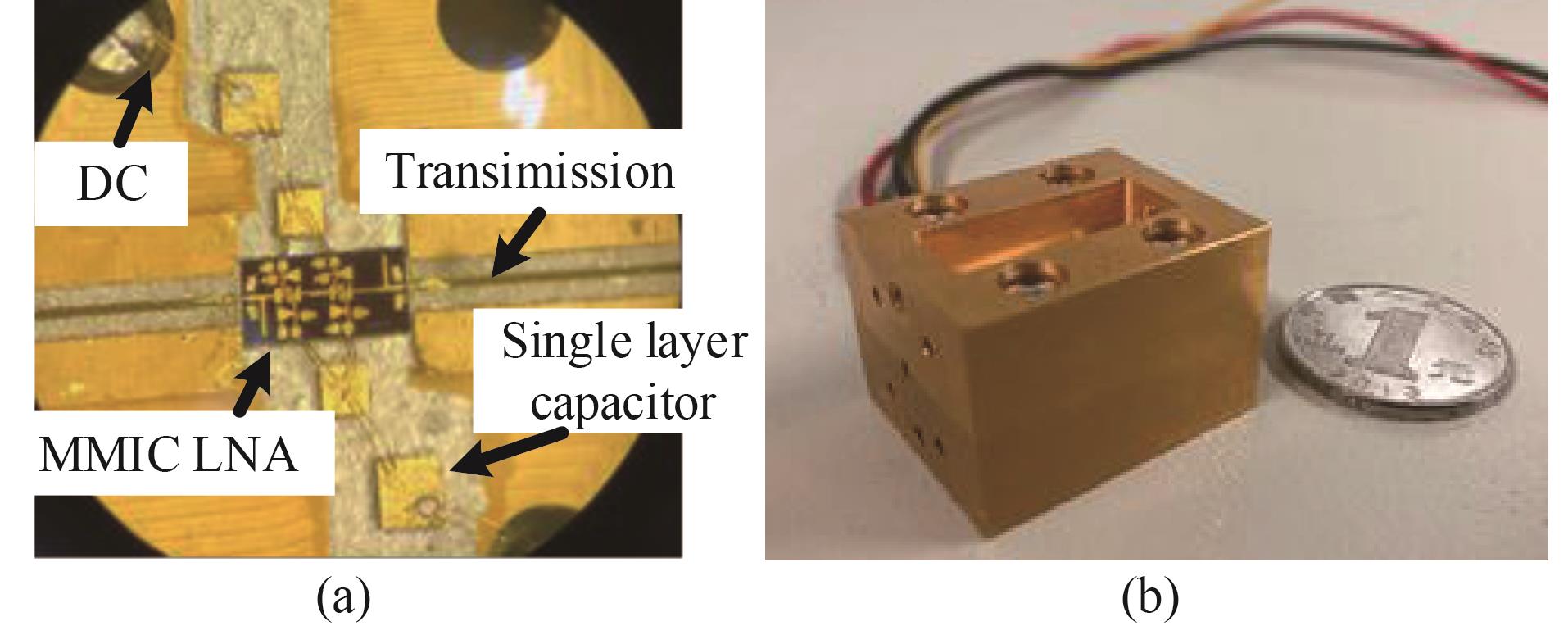
For improving the sensitivity and achieving good signal-to-noise ratio (SNR), a low noise amplifier is an essential need of every radiometer system. The better that noise performance is the weaker signals can be received and analyzed which correlates directly with the sensitivity or range of imaging systems. Improving the noise performance of a receiver is main job of a LNA. The amplifier circuit has been manufactured using 100-nm gate length InP HEMT technology in Ref.13. In this paper, the selected amplifier has been assembled in an E-plan split-block waveguide package. The package design mainly includes transitions from microstrip to rectangular waveguide. The outer dimensions of the block are 30 mm×20 mm×25 mm and the LNA chips and chip capacitors are attached to the block with conductive epoxy glue. Figure 1 shows the photograph of the split-block module with MMIC, waveguide to microstrip transitions.
![]()
Figure 1.(a) The split-block module with MMIC, (b) the photo of the LNA module
The LNA module was measured using Rohde & Schwarz ZVA50 network analyzer with Rohde & Schwarz ZC170 (110~170 GHz) frequency extenders. The measurement results for the packaged LNA are shown in Fig. 2. The LNA module exhibits maximum gain of 10.8 dB at 145 GHz and 3 dB bandwidth is about 7 GHz from 137 GHz to 144 GHz. The measured input return loss S11 better than 5 dB and output return loss S22 better than 8.5 dB in the frequency from 125 GHz to 155 GHz. Due to the waveguide flange is not suitable, between the output port and test equipment have a split, the fluctuate of S22 is greatly with frequency. Another reason may be the wire-bonding at output port causes the matching performance changed. As shown in Fig. 2, the tendency of packaged S21 curve is same as the on-chip measured and its value is worse than the on-chip measurement about 5 dB. Due to the pad size is limited, a 25-µm bonding wire was used for connection is the main reason of the deterioration of the LNA module performance. The noise figure is about 5 dB and the DC power consumption is about 32.4 mW with a drain voltage of Vds=1.2 V.
![]()
Figure 2.LNA packaged measured S-parameters, on-chip S21
2 Detector module
The millimeter wave detectors play an important role in many millimeter wave systems such as power detection devices, direct detection receivers and imaging system. With the development of millimeter wave technologies, there is pressing need of compact and highly sensitive detector that operated at room temperature. Schottky diodes with the properties of low parasitic capacitance and series resistance provides an efficient solution for millimeter wave detection under room temperature [
A D-band detector was designed based on zero-bias Schottky barrier diode HSCH-9161 and Fig. 3 shows the schematic diagram of the detector. Figure 4 shows small signal linear model of the HSCH-9161 that include junction resistance Rj, junction capacitance Cj, series resistance Rs, parasitic capacitance Cs and parasitic inductance Ls.
![]()
Figure 3.Schematic diagram of D-band detector
![]()
Figure 4.Small signal linear model of HSCH-9161
All passive networks including waveguide to microstrip, matching network and low pass filter of the detectors are analyzed and designed by HFSS and fabricated on 50-µm quartz substrate. The simulation model and simulated result of input waveguide to microstrip transition is shown in Fig.5. As shown in Fig.5(b), the transmission loss below 0.15 dB and the return loss above 20 dB from 118 to 172 GHz. For isolating the detector signal (DC or low frequency signal) from RF signal, a low pass filter (LPF) is designed as indicated in Fig.6. From the simulated result of the LPF that presented in Fig.6(b), the rejection above 20 dB in full D-band and the transmission loss is below 0.15 dB in low frequency.
![]()
Figure 5.(a) Simulation model of input waveguide to microstrip, and (b) the simulated result
![]()
Figure 6.(a)Simulation model of low pass filter, and (b) the simulated result
Finally, the quartz substrate was mounted to the waveguide block with conductive epoxy glue. The outer dimensions of the block are 20 mm×19 mm×15 mm and Fig.7 shows the photo of the detector.
![]()
Figure 7.Photo of the detector
The diagram of voltage sensitivity measurement setup for the detector is shown in Fig.8. A CETC-41 microwave source AV1464C with AV82406B (110~170 GHz) frequency extenders were employed to provide the D-band power, which was measured by Erickson power meter. An attenuator was adopted for ensuring the detector was operating in the square–law region that to keep the input power under -12 dBm. Finally, the output voltage was detected by digital multimeter.
![]()
Figure 8.Diagram of sensitivity measurement setup for detector
The voltage sensitivity (Rv) of the detector can be calculated by
where Vout is the voltage measured by digital multimeter and Pin is the incident RF power presented by Erickson power meter. The sensitivity of the detector is estimated by this method and the result is shown in Fig.9. The measurement shows that the voltage sensitivity is larger than 400 mV/mW between 110~140 GHz, larger than 120 mV/mW in D-band and the maximal value reaches about 1600 mV/mW@110 GHz.
![]()
Figure 9.The measured sensitivity of the detector
When the detector is working, the effective detection current mainly refers to the current through the junction resistance Rj. Due to the junction capacitance Cjand Rj are in parallel, it plays a certain bypass function, resulting in a decrease in sensitivity. Also, the series resistance Rs divides the valid voltage. The operate frequency f of the diode can be defined as
As the frequency increases, the value of Rj decreases. Because the diode selected in this paper is suitable for W-band, as the frequency increases, the Rj will drop sharply, and the cut-off frequency is close to the D-band, so that most of the signal energy received by the diode is applied to Rs, which decreases Rj. The diode nonlinearity basically disappears, eventually causing its performance to be severely degraded.
3 Imaging experiments
An imaging system that based on LNA module, detector module and standard horn antenna has been designed to demonstrate the imaging performance of our radiometer front-end. Based on the above module, the schematic diagram of imaging experiment and the measurement setup are shown in Figs.10-11. As shown in Fig.11, the imaging system is composed by D-band source, imaging object and the radiometer front-end. The D-band source is comprised by self-designed ×12 multiplication chains, providing a continuous output of 8mW at room temperature. The source is amplitude modulated with a modulation frequency of 10 kHz and an amplitude modulation depth of 100% and the RF signal is radiated through the standard horn antenna. The imaging object is a 15 cm×15 cm metal square with T shape hole, which moves with the 2D guide screw to achieve scanning. The receiving antenna is separated from the object by 15 cm, which means the resolution is 1.5 cm×1.5 cm. When transmitted through the T-shape area, the RF signal is detected by radiometer front-end and then read out by the spectrometer with a high potential, in other areas of the square structure, the signal is reflected and outputs low potential. The recorded potential in spectrometer will be numerically mapping to a grey scale for imaging.
![]()
Figure 10.Principle of imaging experimental
![]()
Figure 11.Photo of the measurement setup
First, we perform the imaging experiments only use detector and antenna and the imaging result is shown in Fig.12. Compared with the real object, the Fig. 12 can clearly show the different characteristics of the T-shape and the outlines are basically same with the T-shape. At the same time, due to the metal edge cannot completely isolate the radiated signal, so some fuzzy points appeared in the T-shape edge area.
![]()
Figure 12.Imaging result of the radiometer front-end without LNA
Then the imaging experiments are performed with LNA module and detector module and the imaging result is shown in Fig.13. Compared Fig.12 with Fig.13, after adding the LNA module to the front-end of the radiometer, there are still some edge blur points, increasing the signal reception intensity and detection output level, improving the signal-to-noise ratio. The contrast to the image is improved, and the imaging result is better.
![]()
Figure 13.Imaging result of the radiometer front-end with LNA
The noise equivalent temperature difference (NETD) is an important figure of merit for determining radiometer sensitivity. NETD is related to the thermal responsibility of the system and can be defined using system parameters as
where τ is the integration time, B is the RF bandwidth, TS is the scene temperature and TR is the receiver noise temperature. Due to the bandwidth of LNA module is about 20 GHz, according to Eq.3, when τ = 1 ms and B = 20 GHz, the ideal NETD of the system are estimated to be about 0.2 K. For better image quality, increasing the bandwidth and decreasing the noise figure of LNA and choosing a diode that suitable for D-band for improving the voltage sensitivity is necessary.
4 Conclusion
In this paper, a D-band direct detection radiometer front-end which consists detector module,low noise amplifier module and standard gain horn antenna is designed and the imaging experiments have been carried out. The D-band detector module is designed and fabricated based on zero-bias Schottky barrier diode HSCH-9161 and the D-band LNA module is packaged with self-designed InP-based LNA MMIC. The imaging experiments are carried out based on this radiometer front-end and the results are compared with or without LNA module. After adding the LNA module the contrast to the image is improved, and the imaging result is better. This radiometer front-end lays a solid foundation for the practical application of the terahertz radiometer.
References
[1] T Kanar, G M Rebeiz. A low-power 136-GHz SiGe total power radiometer with NETD of 0.25 K. IEEE Transactions on Microwave Theory & Techniques, 64, 906-914(2016).
[2] C Viegas, B Alderman, J Powell. Millimeter wave radiometers for applications in imaging and nondestructive testing(2016).
[3] Q J Gu, Z Xu, A Tang. A D-band passive imager in 65 nm CMOS. IEEE Microwave and Wireless Components Letters, 22, 263-265(2012).
[4] E Dacquay, A Tomkins, K H K Yau. D-band total power radiometer performance optimization in an SiGe HBT technology. IEEE Transactions on Microwave Theory & Techniques, 60, 813-826(2012).
[5] C Viegas, B Alderman, J Powell. Millimeter wave radiometers for applications in imaging and nondestructive testing(2016).
[6] J Dunne, C Mann. Detection of corrosion under paints and insulating layers using passive millimetre wave imaging(2016).
[7] R. Ben Yishay, D Elad. ,
[8] A I M Hassanin, A S E Shaaban, F E Abd El-Samie. Medical applications of image reconstruction using electromagnetic field in terahertz frequency range. Turkey, 1-4(2019).
[9] T Skotnicki, W Knap. Terahertz technologies and applications. Poland, 34-37(2019).
[10] M O AlNabooda, R M Shubair, N R Rishani. Terahertz spectroscopy and imaging for the detection and identification of Illicit drugs, 1-4(2017).
[11] E Aguilar, A Hagelauer, R Weigel. A 155 GHz low-power total power radiometer in a 130 nm SiGe technology, 343-346(2018).
[12] R B Yishay, D Elad. D-band Dicke-radiometer in 90 nm SiGe BiCMOS technology. HI, 1957-1960(2017).

Set citation alerts for the article
Please enter your email address
© Copyright 2018-2021 | Chinese Laser Press. All Rights Reserved 沪ICP备15018463号-20