Jun LIU, Rui-Liang SONG, Ning LIU, Shi-Xiong LIANG. Design and realization of InP-based resonant tunneling diode THz oscillator[J]. Journal of Infrared and Millimeter Waves, 2022, 41(2): 443
Copy Citation Text
An oscillator above 1 THz is designed and realized using InP-based resonant tunneling diode (RTD) and an on-chip antenna with Si-lens. The RTD model was built and studied with Silvaco software. The influences of the doping concentration of emitter, the thickness of barrier layer, space layer, and well layer on the DC characteristics of the device have been analyzed. The DC measurement of the RTD shows the peak current density Jp = 359.2 kA/cm2, the valley current density Jv = 135.8 kA/cm2, and the peak-to-valley current ratio (PVCR) = 2.64. According to the measurement, the maximum RF output power and oscillation frequency (fmax) are theoretically calculated, which are 1.71 mW and 1.49 THz, respectively. The oscillator with an on-chip bow-tie antenna and RTD is packaged with Si-lens. The measurement shows the output power is 2.57 μW at an operation frequency of above 1 THz, the DC power consumption is 8.33 mW. This is the first reported oscillator of frequency above 1 THz in domestic.
The terahertz(THz)frequency band(0.3~10 THz)has attracted fast-growing research interests due to its many possible applications,such as imaging systems for radar or security imaging,spectroscopy in chemistry and biotechnology and high-data-rate communications [1-6]. The compact and coherent solid-state THz signal sources are considered to be the key components for these applications. Compared with any other traditional electronic devices such as field-effect or bipolar transistors(MOSFETs,HEMTs or HBTs),or diode technologies(IMPATT,Gunn,etc.),the resonant tunneling diodes(RTDs)have also been considered as one of the most promising candidates for THz oscillators at room temperature [7-10]. The advantages of RTDs include the facts that they can exhibit the highest oscillation frequency of the inherent negative differential conductance(NDC)due to the resonant tunneling among the electronic devices and consume low power,as well as the output power is easily modulated through the bias network and can operate at room temperature.
In this paper,we propose and fabricate a THz oscillator with InP-based RTD and dielectric lens antenna. The influences of material structure including the doping concentration of emitter,the thickness of barrier layer,space layer,and well layer on the DC characteristics are analyzed by Silvaco software. Excellent DC characteristics of the RTD are demonstrated with Jp = 359.2 kA/cm2,Jv = 135.8 kA/cm2,and PVCR = 2.64. The oscillator is packaged with Si-lens and exhibits the output power of 2.57 μW at an operation frequency above 1 THz.
1 RTD device
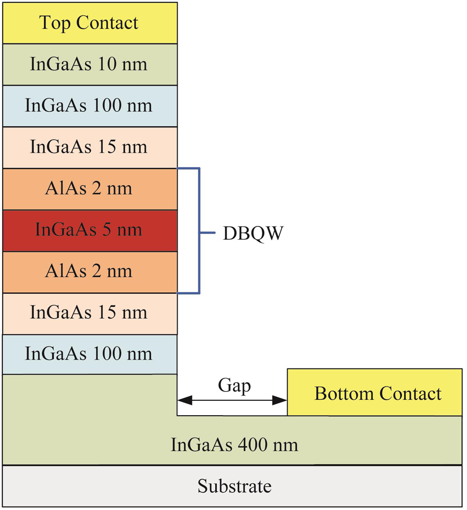
RTDs are commonly realized in GaAs and InP. Compared with GaAs,InP material system offers better properties in the conduction band offset,the electron effective mass. In0.53Ga0.47As can also be highly doped when used as the RTD device electrodes to reduce the Ohmic contact resistance. The material system for the RTD device utilized in this project is InGaAs/AlAs. InP-based RTD device is typically consisted of a narrow bandgap material(4∼6 nm thick quantum well)sandwiched between two thin wide bandgap materials(1∼3 nm AlAs barriers),making up a double barrier quantum well(DBQW)structure. The structure is completed by lightly doped InGaAs spacer layers,n-type emitter/collector layers,and highly doped InGaAs contact layers on each side of the DBQW,as shown in Fig. 1.
Composition
Doping/ cm-3
Thickness/nm
InP Substrate
n+-In0.7Ga0.3As
2*1019
8
n+-In0.53Ga0.47As
2*1019
15
n+-In0.53Ga0.47As
3*1018
25
un-In0.53Ga0.47As
20
un-AlAs
1.2
un-In0.8Ga0.2As
5
un-AlAs
1.2
un-In0.53Ga0.47As
2
n+-In0.53Ga0.47As
3*1018
20
n+-In0.53Ga0.47As
2*1019
400
un-In0.53Ga0.47As
200
Table 1. The layer structure of the RTD device used in this study
The 2D structure of the device is defined in Deckbuild based on the material structure as shown in Fig. 1 by using the Atlas,which a device simulation product originating simulated from Silvaco. The relationship between the epi-layer structure and DC characteristics has been researched on the doping concentration of emitter,the thickness of barrier layer(tB),well layer(tW)and spacer layer(tS). In order to observe the relationship between the material structure and DC characteristics more intuitively,the peak current(IP)and peak voltage(VP)of the device are mainly analyzed,as shown in Fig. 2. The simulation results in Fig. 2 shows that the performance of RTD devices is closely related to the epitaxial material structure. In order to realize a high-power,high-frequency RTD device,the electrical characteristics of the device is optimized mainly by optimizing the negative differential conductance region(NDR)in the I-V curve in this design. After optimization,the RTD material structure designed in this study is shown in Table 1.
The RTD epi-material is grown on a 3-inch wafer using molecular beam epitaxy(MBE). The photograph of the manufactured InP-based RTD device with an emitter area of 12 μm2 is shown in Fig. 3(a). Characterization of the device was done by on-wafer measurements with B1500A Semiconductor Device Parameter Analyzer at room temperature. The on-wafer measured I-V characteristic of the RTD device is depicted in Fig. 3(b). The RTD shows peak voltage Vp=0.91 V,peak current Ip=43.1 mA,peak current density Jp=Ip/A=359.2 kA/cm2,and peak-to-valley current ratio PVCR=Ip/Iv=2.64.
Figure 3.(a)Photo of the fabricated RTD,(b)measured I-V characteristic of the RTD device
Figure 4 shows the small-signal equivalent circuit of the RTD. The total series resistance(Rs)of the diode includes ohmic contact resistance,spreading resistance,and resistance due to the epitaxial layer. The Rs ≈4.8 Ω is estimated from transmission line measurements(TLM). The self-capacitance(Cn)represents the charging and discharging effect of electrons at the semiconductor depletion regions. The Cn ≈11 fF is measured by B1500A. The quantum-well inductance(Lqw)represents the electron dwell time in quantum well and will not limit the oscillator frequency [11].
The frequency dependent impedance of the RTD is given by Eq. 1.
.
The maximum oscillation frequency(fmax)of the RTD is defined as the frequency where R(f) becomes zero,as given by Eq. 2.
π ,
Equation 2 simplifies to Eq. 3 when Lqw is assumed to be negligibly small.
π ,
The RTD negative conductance(Gn)is given by
,
where △I=Ip-Iv,△V=Vp-Vv.
The maximum available RF output power(Pmax)that a RTD-based oscillator can deliver to the load,which is given by
.
According to Eqs. 3-5,the theoretical fmax of the RTD is evaluated to be 1.49 THz and the theoretical Pmax=1.71 mW. The DC measurement results of the RTD device and theoretical oscillation frequency and maximum RF output power are summarized in Table 2.
3 Bow-tie antenna
Bow-tie antenna is a widely used wideband antenna in terahertz band. The proposed bow-tie shape THz antenna is shown in Fig. 5(a)and patterned over 25 µm InP substrate. Due to the lower gain of the proposed antenna,a silicon lens is mounted over the antenna as depicted in Fig. 5(b). The simulation of the proposed antenna is carried out in CST Microwave Studio. Fig. 6 shows the variation of the Voltage Standing Wave Ratio(VSWR)and gain of the proposed antenna with Si-lens which indicates more than 200 GHz impedance bandwidth spanning from 0.9 to 1.1 THz and13.7 dBi gain.
Figure 5.(a)schematic of the proposed bow-tie antenna,(b)antenna with Si-lens mounting
Figure 7 presents the package configuration of the quasi-optical RTD oscillator. It consists of RTD oscillator by integrating RTD with a bow-tie antenna,a highly resistive Si-lens and a low-frequency PCB. The fabricated chip is mounted on Si-lens and wire-bonded with Au wires with a diameter of 50 μm onto PCB for the measurements of the oscillation characteristics.
Figure 8 shows the RTD oscillator packaged with PCB and the detail of RTD oscillator. The THz signal is generated from the RTD oscillator and radiate into air through Si-lens.
Figure 8.The photograph of the packaged oscillator
In order to characterize the performances of the fabricated oscillator,the room temperature measurement is performed and the block diagram of the measurement scheme is shown in Fig. 9(a). Due to lacking 1 THz spectrum analyzer,0.75~1.1 THz horn antenna and WR0.65(1.1~1.7 THz)convert waveguide are used with PM5 for measuring the output power and frequency as shown in Fig. 9(b). The best performances of the fabricated oscillator are obtained at an applied bias voltage of 0.95 V with a current of 8.7 mA. A peak output power of 2.57 μW is obtained above 1 THz. The DC power consumption of the RTD oscillator is 8.33 mW,while the DC-to-RF power efficiency is 0.0308% at the operation frequency.
Figure 9.(a)Block diagram of measurement scheme,(b)photo of the test environment
A THz RTD oscillator is designed and fabricated based on InP RTD MMIC technology. The RTD device shows theoretically calculated maximum RF output power of 1.71 mW and fmax of 1.49 THz. The oscillator shows an output power of 2.57 μW with a DC power consumption of 8.33 mW above 1 THz. This work shows the potential of the RTD oscillator topology as a practical THz signal source for future THz applications. To our knowledge,this is the first reported oscillator of frequency above 1 THz in domestic.
References
[1] Jun LIU, Wei HE, Hai-Dong QIAO et al. The study and application of D-band radiometer front-end. Journal of Infrared Millimeter Waves, 39, 704-708(2020).
[2] Ju-Xiu WU, Lei YANG, Fang-Li DOU et al. The detection capability to ice clouds forsSpace-borne terahertz dual-frequency radar. Journal of Infrared Millimeter Waves, 39, 718-727(2020).
[3] Jing-Yuan CHEN, Zhong-Xi LIN, Qi LIN et al. Design and simulation of dual-frequency terahertz antenna for wireless communication by photo mixing. Journal of Infrared Millimeter Waves, 38, 493-498(2019).
[4] Yi-Lin YANG, Bo ZHANG, Dong-Feng JI, Yi-Wei WANG, Xiang-Yang ZHAO, Yong FAN. A wideband terahertz planar Schottky diode fourth-harmonic mixer with low LO power requirement. Journal of Infrared Millimeter Waves, 39, 540-546(2020).
[6] Song-Zhuo LIU, Wei-Hua YU, Chang-Jiang DENG et al. Recent progress of research on terahertz signal modulation technology for communication systems. Radio Communications Technology, 47, 44-50(2021).
Jun LIU, Rui-Liang SONG, Ning LIU, Shi-Xiong LIANG. Design and realization of InP-based resonant tunneling diode THz oscillator[J]. Journal of Infrared and Millimeter Waves, 2022, 41(2): 443