• Acta Optica Sinica
  • Vol. 40, Issue 10, 1031001 (2020)
Qian Zhao1、2, Zhuo Li1、2, Xin Wang1、2、*, Defang Li1、2, and Liqiang Xu1、2
Author Affiliations
  • 1School of Optics and Photonics, Beijing Institute of Technology, Beijng 100081, China
  • 2Beijing Key Lab for Precision Optoelectronic Measurement Instrument and Technology, Beijing 100081, China
  • show less
    DOI: 10.3788/AOS202040.1031001 Cite this Article Set citation alerts
    Qian Zhao, Zhuo Li, Xin Wang, Defang Li, Liqiang Xu. Spatial Resolution of Infrared Scene Projector Chip with Periodical Microstructure[J]. Acta Optica Sinica, 2020, 40(10): 1031001 Copy Citation Text show less
    Structural diagram of infrared scene projector chip
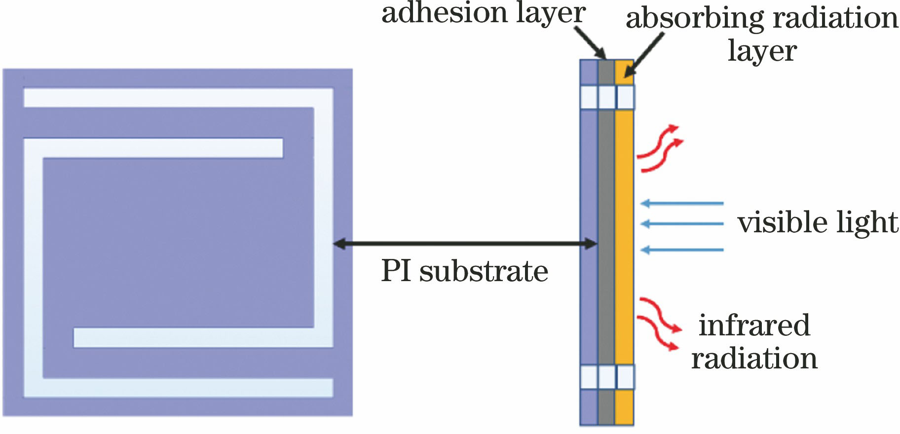
    Fig. 1. Structural diagram of infrared scene projector chip
    Principle block diagram of spatial resolution measurement
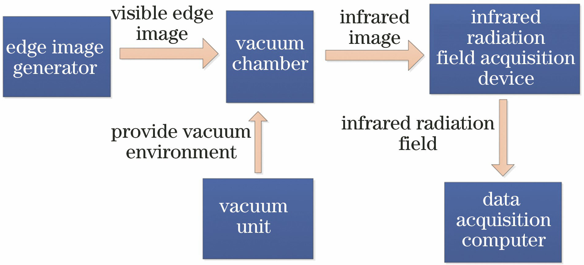
    Fig. 2. Principle block diagram of spatial resolution measurement
    Temperature distribution in chip plane
    Fig. 3. Temperature distribution in chip plane
    Temperature gradient in y-direction
    Fig. 4. Temperature gradient in y-direction
    Temperature distribution calculation model of MEMS chip with periodical microstructure
    Fig. 5. Temperature distribution calculation model of MEMS chip with periodical microstructure
    Distribution of radiation intensity along x-direction
    Fig. 6. Distribution of radiation intensity along x-direction
    Process diagram of MTF curve calculation
    Fig. 7. Process diagram of MTF curve calculation
    Schematic of microstructure used for contact area ratio analysis. (a) 2D diagram of microstructure; (b) 3D diagram of microstructure
    Fig. 8. Schematic of microstructure used for contact area ratio analysis. (a) 2D diagram of microstructure; (b) 3D diagram of microstructure
    Thermal radiation intensity distributions along x-direction of chips with different contact area ratios
    Fig. 9. Thermal radiation intensity distributions along x-direction of chips with different contact area ratios
    MTF curves of microstructured chips with different contact area ratios
    Fig. 10. MTF curves of microstructured chips with different contact area ratios
    Schematic of microstructure used for filling factor analysis
    Fig. 11. Schematic of microstructure used for filling factor analysis
    Thermal radiation intensity distributions of microstructured chips with different filling factors
    Fig. 12. Thermal radiation intensity distributions of microstructured chips with different filling factors
    MTF curves of microstructured chips with different filling factors
    Fig. 13. MTF curves of microstructured chips with different filling factors
    In-plane microstructures of infrared scene projector chips. (a) Contact area ratio of 0.20; (b) contact area ratio of 0.46
    Fig. 14. In-plane microstructures of infrared scene projector chips. (a) Contact area ratio of 0.20; (b) contact area ratio of 0.46
    Sample photo of infrared scene projector chip
    Fig. 15. Sample photo of infrared scene projector chip
    Microscope images of periodical microstructure. (a) Contact area ratio of 0.2; (b) contact area ratio of 0.46
    Fig. 16. Microscope images of periodical microstructure. (a) Contact area ratio of 0.2; (b) contact area ratio of 0.46
    Experimental device diagram of spatial resolution measurement
    Fig. 17. Experimental device diagram of spatial resolution measurement
    Measurement results obtained by infrared thermal imager. (a) Thermal radiation intensity distribution on chip surface; (b) temperature distribution along x-direction
    Fig. 18. Measurement results obtained by infrared thermal imager. (a) Thermal radiation intensity distribution on chip surface; (b) temperature distribution along x-direction
    Radiation intensity distribution curves along x-axis of two chip samples
    Fig. 19. Radiation intensity distribution curves along x-axis of two chip samples
    MTF curves of two infrared scene projector chip samples
    Fig. 20. MTF curves of two infrared scene projector chip samples
    Qian Zhao, Zhuo Li, Xin Wang, Defang Li, Liqiang Xu. Spatial Resolution of Infrared Scene Projector Chip with Periodical Microstructure[J]. Acta Optica Sinica, 2020, 40(10): 1031001
    Download Citation