
Yifu Lin, Xianzhao Yang, Xiangcheng Li. Design of Thin Wideband Absorber Based on Lossy Capacitive Surface of Dipole Square Ring Crossed Element[J]. Acta Optica Sinica, 2023, 43(3): 0322001
- Acta Optica Sinica
- Vol. 43, Issue 3, 0322001 (2023)
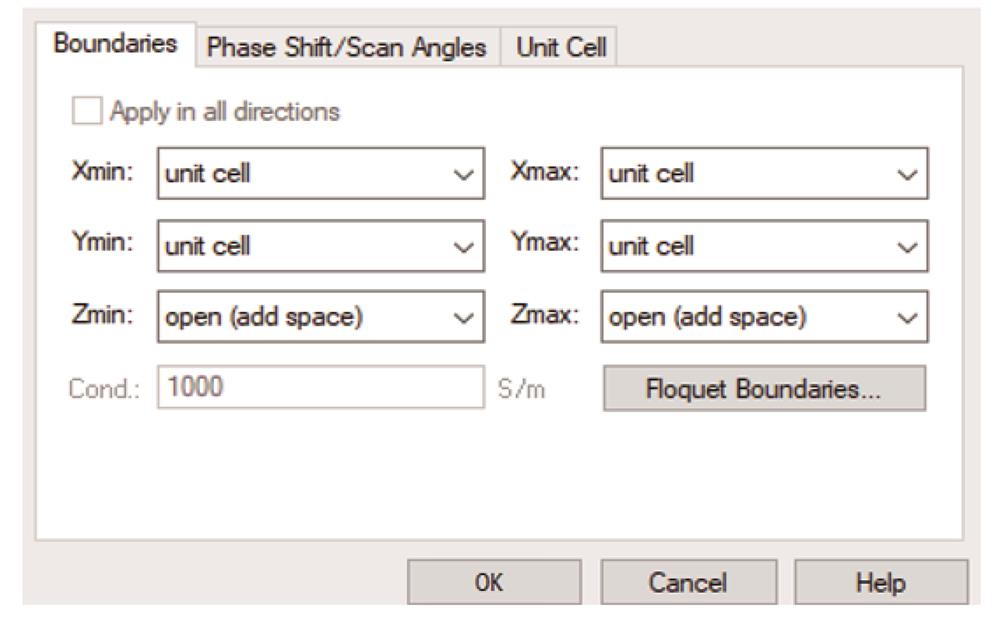
Fig. 1. Boundary condition setting for CST
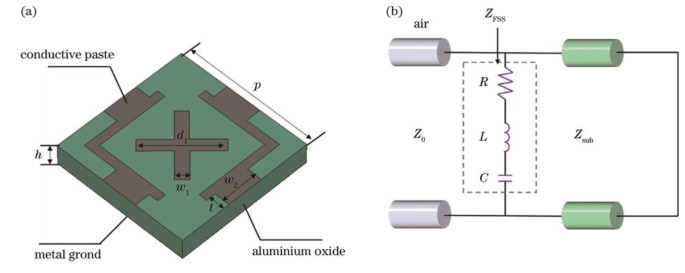
Fig. 2. Structural diagram and equivalent circuit diagram of metamaterial absorber. (a) Structural diagram; (b) equivalent circuit diagram
Fig. 3. Structural diagrams of three different FSSs
Fig. 4. Reflection coefficients of FSSs with three different structures
Fig. 5. Reflectivity curves of metamaterial absorber under with different parameters. (a) h; (b) R
Fig. 6. Reflectivity of designed absorber for different oblique incidence angles in TE and TM polarization modes
Fig. 7. Equivalent medium model
Fig. 8. Equivalent electromagnetic parameters. (a) Equivalent permittivity; (b) equivalent permeability; (c) equivalent impedance
Fig. 9. Current distribution of absorber at resonant frequency. (a) Surface current of FSS; (b) surface current of dielectric backplane; (c) surface current flow during magnetic resonance
Fig. 10. Electromagnetic loss at 12.7 GHz absorption peak. (a) TE mode of square ring crossed element; (b) TM mode of square ring crossed element; (c) TE mode of T-shaped square ring crossed element; (d) TM mode of T-shaped square ring crossed element; (e) TE mode of notched T-shaped square ring crossed element; (f) TM mode of notched T-shaped square ring crossed element
Fig. 11. Actual picture and measured and simulated results of designed absorber. (a) Actual picture; (b) measured and simulated results
|
Table 1. Performance comparison of designed absorber in this paper with those reported in other literatures

Set citation alerts for the article
Please enter your email address
© Copyright 2018-2021 | Chinese Laser Press. All Rights Reserved 沪ICP备15018463号-20