• Opto-Electronic Advances
  • Vol. 5, Issue 5, 210094 (2022)
Peihui Li1, Yijian Chen1, Boyu Wang1, Mengmeng Li1, Dong Xiang1、*, Chuancheng Jia1、*, and Xuefeng Guo1、2、*
Author Affiliations
  • 1Center of Single-Molecule Sciences, Institute of Modern Optics, Tianjin Key Laboratory of Micro-scale Optical Information Science and Technology, Frontiers Science Center for New Organic Matter, College of Electronic Information and Optical Engineering, Nankai University, Tianjin 300350, China
  • 2Beijing National Laboratory for Molecular Sciences, State Key Laboratory for Structural Chemistry of Unstable and Stable Species, College of Chemistry and Molecular Engineering, Peking University, Beijing 100871, China
  • show less
    DOI: 10.29026/oea.2022.210094 Cite this Article
    Peihui Li, Yijian Chen, Boyu Wang, Mengmeng Li, Dong Xiang, Chuancheng Jia, Xuefeng Guo. Single-molecule optoelectronic devices: physical mechanism and beyond[J]. Opto-Electronic Advances, 2022, 5(5): 210094 Copy Citation Text show less
    Diarylethene units used in single-molecule switches.(a) Diarylethene photoisomerization mechanism. (b) Potential energy curves of the molecular switching. The switching process is initiated by an excitation to the first excited state. (c) Diarylethene bridged between the electrode ends. (d) Molecular structures with special design for single-molecule switches. (e) A graphene-diarylethene-graphene single-molecule switch. (f) Self-assembled monolayer devices with diarylethene units. (g) Molecular isomerization under external controls of electrochemical potential and light irradiation. Figure reproduced with permission from: (a) ref.24, American Chemical Society; (b) ref.26, American Physical Society; (c) ref.27, American Chemical Society; (d) ref.28, John Wiley and Sones; (e) ref.7, American Association for the Advancement of Science; (f) ref.30, American Chemical Society; (g) ref.32, under a Creative Commons Attribution 3.0 Unported Licence.
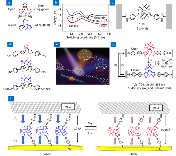
    Fig. 1. Diarylethene units used in single-molecule switches.(a) Diarylethene photoisomerization mechanism. (b) Potential energy curves of the molecular switching. The switching process is initiated by an excitation to the first excited state. (c) Diarylethene bridged between the electrode ends. (d) Molecular structures with special design for single-molecule switches. (e) A graphene-diarylethene-graphene single-molecule switch. (f) Self-assembled monolayer devices with diarylethene units. (g) Molecular isomerization under external controls of electrochemical potential and light irradiation. Figure reproduced with permission from: (a) ref.24, American Chemical Society; (b) ref.26, American Physical Society; (c) ref.27, American Chemical Society; (d) ref.28, John Wiley and Sones; (e) ref.7, American Association for the Advancement of Science; (f) ref.30, American Chemical Society; (g) ref.32, under a Creative Commons Attribution 3.0 Unported Licence.
    Azobenzene units used in single-molecule switches. (a) Structures of trans and cis isomers of azobenzene. (b) Azobenzene as the core unit in the macromolecule. (c) Chemical structures of molecules whose configurational change of the azobenzene unit occurs directly in the molecular backbone. (d) Schematic of azobenzene as the side group of bridging molecule in the junction. (e) Dipole projection on the molecular backbone. The arrow denotes the direction of the dipole projection. (f) Four different conformational states due to the asymmetry caused by the introduction of additional azobenzene side group in cis form in the terphenyl backbone. (g) Vertical distance between two graphene electrodes is regulated by the conformational changes in aryl azobenzene molecules with light irradiation. (h) Vertical tunneling self-assembled monolayer device with an azobenzene derivative on Au electrode. Figure reproduced with permission from: (a, c) ref.33, (b) ref.34, (f) ref.36, John Wiley and Sons; (d, e) ref.35, under a Creative Commons Attribution 4.0 International License; (g) ref.37, Springer Nature; (h) ref.38, American Chemical Society.
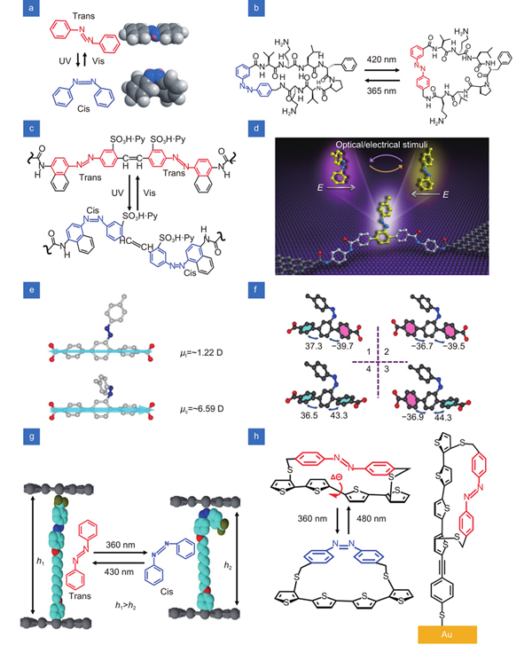
    Fig. 2. Azobenzene units used in single-molecule switches. (a) Structures of trans and cis isomers of azobenzene. (b) Azobenzene as the core unit in the macromolecule. (c) Chemical structures of molecules whose configurational change of the azobenzene unit occurs directly in the molecular backbone. (d) Schematic of azobenzene as the side group of bridging molecule in the junction. (e) Dipole projection on the molecular backbone. The arrow denotes the direction of the dipole projection. (f) Four different conformational states due to the asymmetry caused by the introduction of additional azobenzene side group in cis form in the terphenyl backbone. (g) Vertical distance between two graphene electrodes is regulated by the conformational changes in aryl azobenzene molecules with light irradiation. (h) Vertical tunneling self-assembled monolayer device with an azobenzene derivative on Au electrode. Figure reproduced with permission from: (a, c) ref.33, (b) ref.34, (f) ref.36, John Wiley and Sons; (d, e) ref.35, under a Creative Commons Attribution 4.0 International License; (g) ref.37, Springer Nature; (h) ref.38, American Chemical Society.
    Other units used in single-molecule switches.(a) DHP/CPD single-molecule junction. (b) DHA/VHF single-molecule junction. (c) SP/MC single-molecule junction. (d) Schematic diagram of a vertical tunneling molecular switch with rGO thin films as the transparent top contact and the molecular structures of DHA and VHF. (e) Single-molecule switches with chirality molecules. The spin-polarization direction of the current switches with the chirality inversion. (f) Schematic diagram of SP SAMs in EGaIn/Ga2O3//SAM/AuTS junctions in their open and closed forms. Figure reproduced with permission from: (a) ref.39, American Chemical Society; (b) ref.40, under a Creative Commons Attribution 4.0 International License; (c) ref.41, American Chemical Society; (d) ref.43, John Wiley and Sons; (e) refs.19, 44, under a Creative Commons Attribution 4.0 International License; (f) ref.42, American Chemical Society.
    Fig. 3. Other units used in single-molecule switches.(a) DHP/CPD single-molecule junction. (b) DHA/VHF single-molecule junction. (c) SP/MC single-molecule junction. (d) Schematic diagram of a vertical tunneling molecular switch with rGO thin films as the transparent top contact and the molecular structures of DHA and VHF. (e) Single-molecule switches with chirality molecules. The spin-polarization direction of the current switches with the chirality inversion. (f) Schematic diagram of SP SAMs in EGaIn/Ga2O3//SAM/AuTS junctions in their open and closed forms. Figure reproduced with permission from: (a) ref.39, American Chemical Society; (b) ref.40, under a Creative Commons Attribution 4.0 International License; (c) ref.41, American Chemical Society; (d) ref.43, John Wiley and Sons; (e) refs.19, 44, under a Creative Commons Attribution 4.0 International License; (f) ref.42, American Chemical Society.
    Photoconductance of single-molecule devices. (a) Schematic illustration of the Au/NH-PTCDI-NH/Au junction under light irradiation. (b) SAM-templated addressable nanogap devices comprised of AminoPyr or SC18. (c) Schematic presentation of the charge transport of a molecular junction affected by the excitation. (d) Bonding geometry of a porphyrin-C60 dyad molecule in the gold-ITO tunnel junction. (e) Schematic diagram of carbon/bilayer/carbon tunneling junctions. (f) Energy level diagram for a BTB–AQ bilayer junction. Figure reproduced with permission from: (a, c) ref.47, American Chemical Society; (b) ref.50, under a Creative Commons Attribution 4.0 International License; (d) ref.49, American Chemical Society; (e, f) ref.51, John Wiley and Sons.
    Fig. 4. Photoconductance of single-molecule devices. (a) Schematic illustration of the Au/NH-PTCDI-NH/Au junction under light irradiation. (b) SAM-templated addressable nanogap devices comprised of AminoPyr or SC18. (c) Schematic presentation of the charge transport of a molecular junction affected by the excitation. (d) Bonding geometry of a porphyrin-C60 dyad molecule in the gold-ITO tunnel junction. (e) Schematic diagram of carbon/bilayer/carbon tunneling junctions. (f) Energy level diagram for a BTB–AQ bilayer junction. Figure reproduced with permission from: (a, c) ref.47, American Chemical Society; (b) ref.50, under a Creative Commons Attribution 4.0 International License; (d) ref.49, American Chemical Society; (e, f) ref.51, John Wiley and Sons.
    Photo-assisted transport mechanism in tunnelling junctions. (a) A vacuum gold tunnelling junction. (b) Plasmonic enhancement of the electromagnetic field in the junctions. (c) Schematic representation of the mechanically controllable break fiber junction chip. The inset shows a zoomed view of the suspended fiber/Cr/Au bridge. (d) Strong shift of the electrode energy level in imidazole single-molecule junctions caused by photon absorption. Figure reproduced with permission from: (a) ref.54, Springer Nature; (b) ref.55, American Chemical Society; (c, d) ref.56, The Royal Society of Chemistry.
    Fig. 5. Photo-assisted transport mechanism in tunnelling junctions. (a) A vacuum gold tunnelling junction. (b) Plasmonic enhancement of the electromagnetic field in the junctions. (c) Schematic representation of the mechanically controllable break fiber junction chip. The inset shows a zoomed view of the suspended fiber/Cr/Au bridge. (d) Strong shift of the electrode energy level in imidazole single-molecule junctions caused by photon absorption. Figure reproduced with permission from: (a) ref.54, Springer Nature; (b) ref.55, American Chemical Society; (c, d) ref.56, The Royal Society of Chemistry.
    “Hot electron” effect of single-molecule devices. (a) Schematic demonstration of an illuminated metal-molecule-metal junction with 4,4′-bipyridine (BP) molecule. (b) Nonradiative decay of SPP with generated hot electrons and holes. (c) Nonequilibrium distribution of hot electrons and holes in biased junctions. (d) Experimental setup and strategy to map hot-carrier energy distributions. (e) Schematic illustration of the real-time observation of the plasmon-induced chemical reaction. Figure reproduced with permission from: (a) ref.59, American Chemical Society; (b–d) ref.62, (e) ref.63, American Association for the Advancement of Science.
    Fig. 6. “Hot electron” effect of single-molecule devices. (a) Schematic demonstration of an illuminated metal-molecule-metal junction with 4,4′-bipyridine (BP) molecule. (b) Nonradiative decay of SPP with generated hot electrons and holes. (c) Nonequilibrium distribution of hot electrons and holes in biased junctions. (d) Experimental setup and strategy to map hot-carrier energy distributions. (e) Schematic illustration of the real-time observation of the plasmon-induced chemical reaction. Figure reproduced with permission from: (a) ref.59, American Chemical Society; (b–d) ref.62, (e) ref.63, American Association for the Advancement of Science.
    Photovoltaic effect in single-molecule devices. (a) A GaAs-molecule-Au molecular junction. (b) Schematic band diagram for the illuminated metal-molecule-semiconductor junction under reverse biases. (c) I–V characteristics of the Au-GaAs junction. Figure reproduced with permission from: (a, b) ref.66, American Chemical Society; (c) ref.67, The Royal Society of Chemistry.
    Fig. 7. Photovoltaic effect in single-molecule devices. (a) A GaAs-molecule-Au molecular junction. (b) Schematic band diagram for the illuminated metal-molecule-semiconductor junction under reverse biases. (c) IV characteristics of the Au-GaAs junction. Figure reproduced with permission from: (a, b) ref.66, American Chemical Society; (c) ref.67, The Royal Society of Chemistry.
    Electroluminescence of plasmon. (a) Photon emission induced by inelastic tunneling through a nano-gap between a sharp Au tip and an Au substrate. (b) Schematic diagram and mechanism diagram of how hot electrons excite plasmon electroluminescence. (c) Illustration of the molecular tunneling junction with a SAM of SCn. (d) Blinking of plasmon sources obtained from molecular tunneling junction with a SC12 SAM. (e) Corresponding spectra of plasmon electroluminescence excited at different biases. Figure reproduced with permission from: (a) ref.71, American Chemical Society; (b) ref.72, (c–e) ref.73, Springer Nature.
    Fig. 8. Electroluminescence of plasmon. (a) Photon emission induced by inelastic tunneling through a nano-gap between a sharp Au tip and an Au substrate. (b) Schematic diagram and mechanism diagram of how hot electrons excite plasmon electroluminescence. (c) Illustration of the molecular tunneling junction with a SAM of SCn. (d) Blinking of plasmon sources obtained from molecular tunneling junction with a SC12 SAM. (e) Corresponding spectra of plasmon electroluminescence excited at different biases. Figure reproduced with permission from: (a) ref.71, American Chemical Society; (b) ref.72, (c–e) ref.73, Springer Nature.
    Electroluminescence from molecules in a STM nanocavity. (a) A single ZnPc molecule in a STM nanocavity, where the Au (111) substrate is covered with sodium chloride. (b) Schematic demonstration of the luminescence mechanism for a neutral ZnPc. (c) STM-induced light emission spectrum (black line) of the ZnPc linear tetramer. (d) Phosphorescence scanning tunnel luminescence map of the PTCDA/NaCl/Ag (111) system. (e) Schematic images of the exciton formation mechanism; the arrows represent electrons. Arrows up and down represent the direction of electron spin. (f) Peak characteristics of fluorescence and phosphorescence. Figure reproduced with permission from: (a, b) ref.77, American Association for the Advancement of Science; (c) ref.80, American Physical Society; (d−f) ref.82, Springer Nature.
    Fig. 9. Electroluminescence from molecules in a STM nanocavity. (a) A single ZnPc molecule in a STM nanocavity, where the Au (111) substrate is covered with sodium chloride. (b) Schematic demonstration of the luminescence mechanism for a neutral ZnPc. (c) STM-induced light emission spectrum (black line) of the ZnPc linear tetramer. (d) Phosphorescence scanning tunnel luminescence map of the PTCDA/NaCl/Ag (111) system. (e) Schematic images of the exciton formation mechanism; the arrows represent electrons. Arrows up and down represent the direction of electron spin. (f) Peak characteristics of fluorescence and phosphorescence. Figure reproduced with permission from: (a, b) ref.77, American Association for the Advancement of Science; (c) ref.80, American Physical Society; (d−f) ref.82, Springer Nature.
    Coupling of molecular electroluminescence and plasmon nanocavity. (a) Two different junction structures: on top of the molecule or in close proximity to the molecule. (b) STM-induced luminescence of the situation that the tip is in close proximity to the molecule which cause Fano resonance. (c) Excitation of molecular fluorescence through intermolecular energy transfer. (d) Schematic illustration of the process of intermolecular energy transfer. (e) Exciton splitting diagram for different coherent dipole–dipole coupling modes. Figure reproduced with permission from: (a, b) ref.83, under a Creative Commons Attribution 4.0 International License; (c, d) ref.86, (e) ref.87, Springer Nature.
    Fig. 10. Coupling of molecular electroluminescence and plasmon nanocavity. (a) Two different junction structures: on top of the molecule or in close proximity to the molecule. (b) STM-induced luminescence of the situation that the tip is in close proximity to the molecule which cause Fano resonance. (c) Excitation of molecular fluorescence through intermolecular energy transfer. (d) Schematic illustration of the process of intermolecular energy transfer. (e) Exciton splitting diagram for different coherent dipole–dipole coupling modes. Figure reproduced with permission from: (a, b) ref.83, under a Creative Commons Attribution 4.0 International License; (c, d) ref.86, (e) ref.87, Springer Nature.
    Electroluminescence in single-molecule junctions. (a) A polythiophene molecular wire suspended between the metal substrate and the tip of STM. (b) Fluorescent junctions with different emitting units suspending between the substrate and the tip of the STM by oligothiophene chains. (c) A single graphene nanoribbon junction. (d) Device structure of the nanotube–molecule–nanotube junction. (e) Chemical structure of the molecule, which consists of a central 2,6-dibenzylamino core-substituted NDI chromophore (blue), two OPE rods (red) and phenanthrene anchor units (green). (f) Energy-level model with the HOMO and LUMO molecular orbitals of the OPE and NDI subunits. Figure reproduced with permission from: (a) ref.90, American Physical Society; (b) ref.91, American Chemical Society; (c) ref.92, American Chemical Society; (d–f) ref.93, Springer Nature.
    Fig. 11. Electroluminescence in single-molecule junctions. (a) A polythiophene molecular wire suspended between the metal substrate and the tip of STM. (b) Fluorescent junctions with different emitting units suspending between the substrate and the tip of the STM by oligothiophene chains. (c) A single graphene nanoribbon junction. (d) Device structure of the nanotube–molecule–nanotube junction. (e) Chemical structure of the molecule, which consists of a central 2,6-dibenzylamino core-substituted NDI chromophore (blue), two OPE rods (red) and phenanthrene anchor units (green). (f) Energy-level model with the HOMO and LUMO molecular orbitals of the OPE and NDI subunits. Figure reproduced with permission from: (a) ref.90, American Physical Society; (b) ref.91, American Chemical Society; (c) ref.92, American Chemical Society; (d–f) ref.93, Springer Nature.
    Peihui Li, Yijian Chen, Boyu Wang, Mengmeng Li, Dong Xiang, Chuancheng Jia, Xuefeng Guo. Single-molecule optoelectronic devices: physical mechanism and beyond[J]. Opto-Electronic Advances, 2022, 5(5): 210094
    Download Citation