
Yueqiang Hu, Xin Li, Xudong Wang, Jiajie Lai, Huigao Duan. Progress of micro-nano fabrication technologies for optical metasurfaces[J]. Infrared and Laser Engineering, 2020, 49(9): 20201035
- Infrared and Laser Engineering
- Vol. 49, Issue 9, 20201035 (2020)
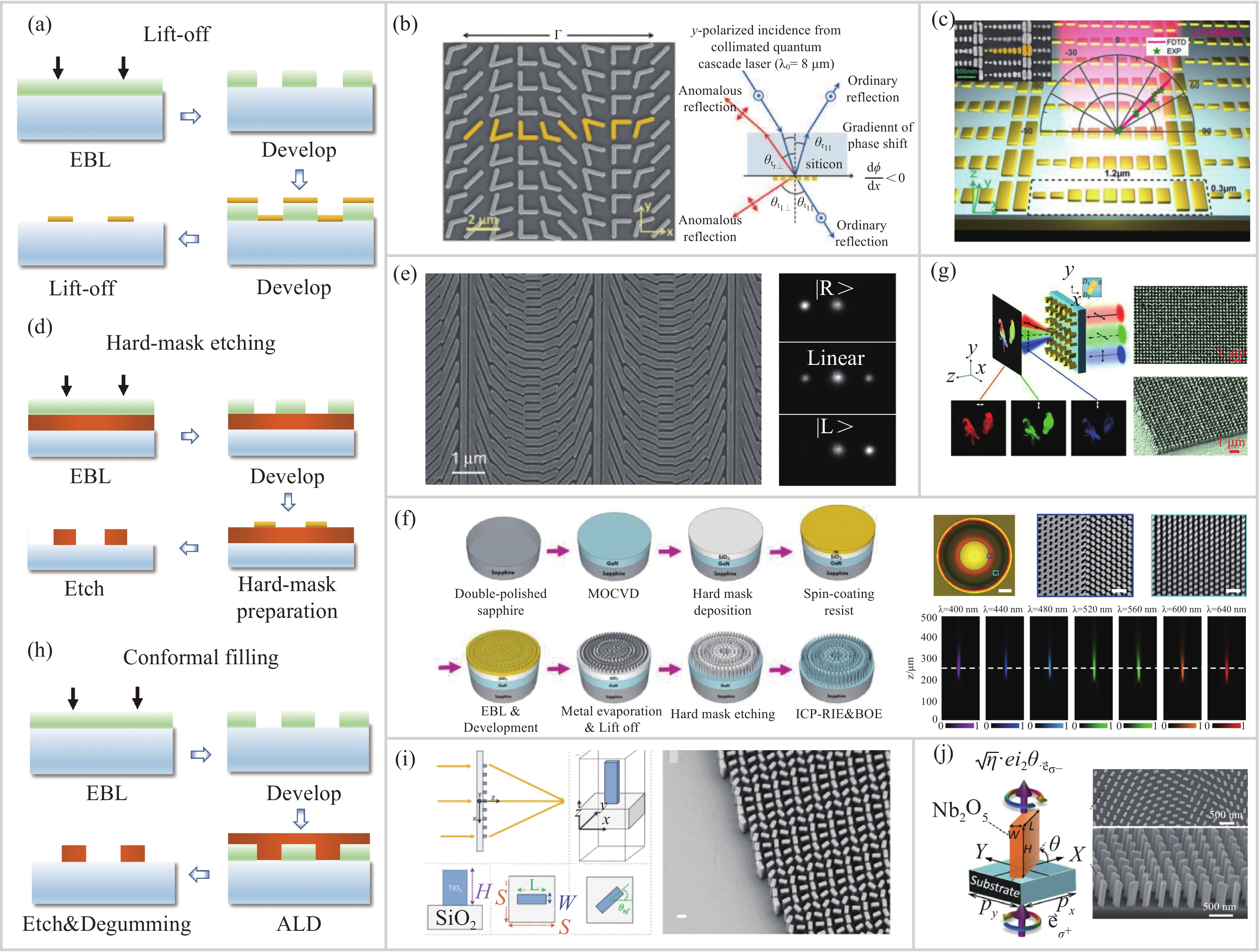
Fig. 1. Fabrication of metasurfaces by electron beam lithography (EBL). (a) Lift-off process for metallic metasurfaces fabrication and its processed (b) transmissive metallic metasurface and (c) reflective metallic metasurface; (d) Hard-mask etching process for dielectric metasurfaces fabrication and its processed (e) Si metasurface, (f) GaN achromatic metalens and (g) TiO2 holographic metasurface; (h) Conformal filling process for dielectric metasurfaces fabrication and its processed (i) TiO2 metalens and (j) Nb2O5 metasurface
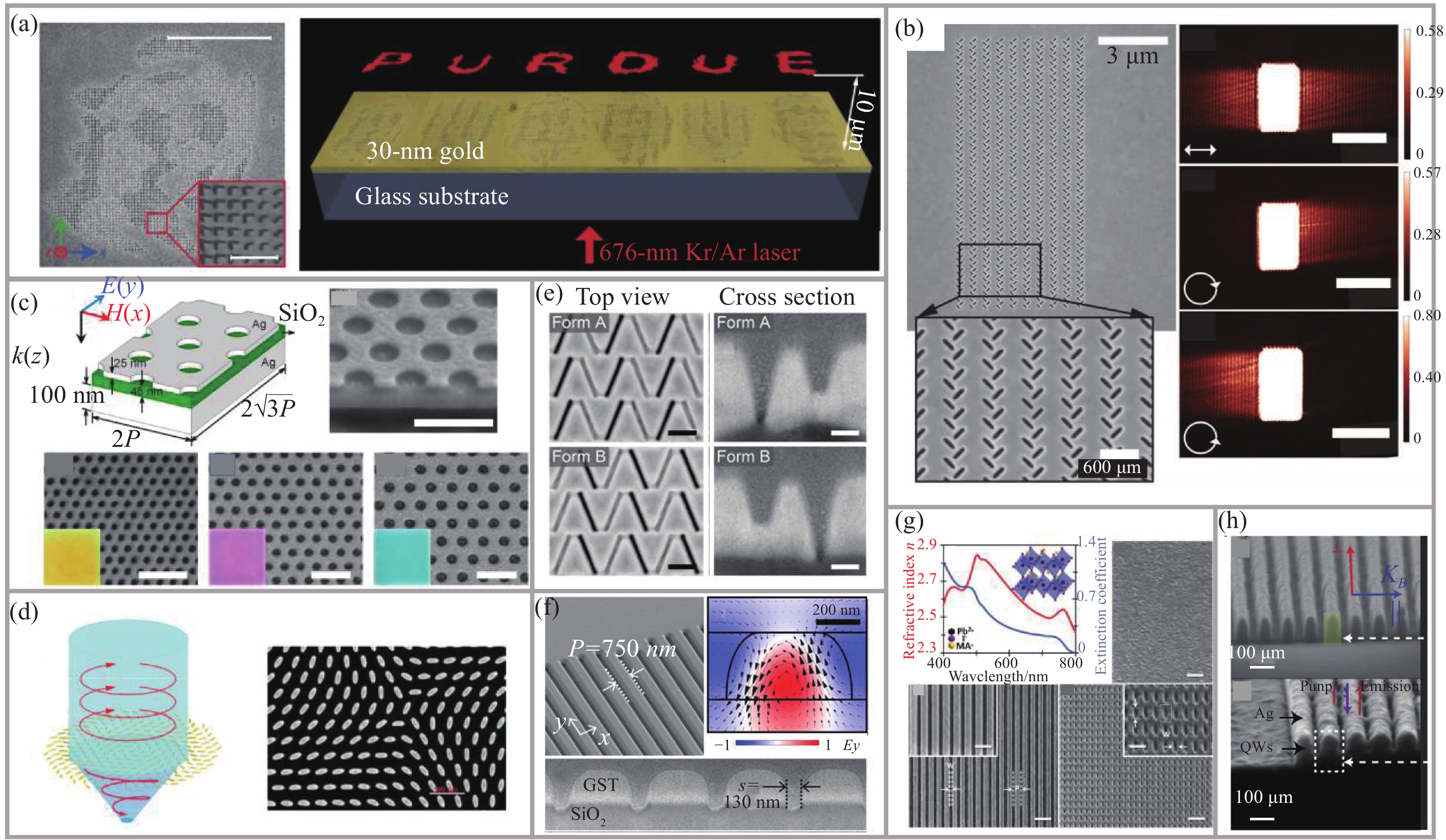
Fig. 2. Fabrication of metasurfaces by focused ion beam (FIB) etching. The metallic nano-hole structures fabricated by FIB is used for (a) holographic metasurface, (b) near-field light field control and (c) structural color modulation; (d) Metallic nanopillar-type metasurface etched by FIB for vortex optical focusing; (e) Metasurface of quasi-3D structure fabricated by FIB. Non-metallic metasurface fabricated by FIB, such as (f) GST phase change material metasurface, (g) perovskite metasurface and (h) metal-dielectric multi-material laminated structure
Fig. 3. Fabrication of metasurfaces by direct laser writing (DLW). (a) Polarization-controllable optical vortex modulation all-dielectric metasurface based on DLW; (b) Schematic diagram of single-step ultrafast laser interference direct writing etching process; (c) Fourier hologram based on ultrafast femtosecond laser etching technology; (d) Two terahertz metasurface with elliptic apertures fabricated by the femtosecond laser slit space control technology on the gold film; (e) 2D perovskite lens fabricated by femtosecond laser; (f) Physical image and SEM image of the new type flat lens whose performance is easy to control based on 2D perovskite nanosheets; (g) SEM images of direct and inverted photonic structure with different symmetry fabricated by two-photon polymerization 3D printing process; (h) Processing principle diagram and SEM image of the nearly perfect infrared spectrum absorption metasurface based on two-photon polymerization 3D printing process; (i) Process flow chart of computer-generated holographic projection based on two-photon polymerization 3D printing process and the schematic diagram of the hologram; (j) Schematic diagram of a Daman grating generating an N ×N dot array in the far field based on two-photon polymerization 3D printing process
Fig. 4. Fabrication of metasurfaces by mask photolithography process. (a) Schematic of metasurface-based half-wave plate by processing directly on Si wafer (left), photograph of the fabricated 12-in Si metasurface wafer and three SEM images of Si pillar array inside the center white squares of the wafer(right); (b) Schematic of color display metasurface by adding a dielectric layer before the photolithography (left), silicon wafers and nanostructures of different sizes, the bottom left is the pattern of color display (right); (c) Flow diagram of photolithography on the transparent glass substrate (left), the fabricated wafer and the enlarged unit pattern(right); (d) Lithography process of the all-glass metasurface with opaque layer (up), the SEM images of the fabricated nanopillars and result of lens(down); (e) Schematic of the metalens by layer transfer technology on glass substrate (left), the schematic of unit structure (right); (f) SEM image of reflective metasurface with a metal layer (left), the schematic of structure of photolithography (right); (g) Schematic of the near-field lithography structure with the reflective plasmonic lens
Fig. 5. Fabrication of metasurfaces by nanoimprint lithography. (a) SEM images of the two kinds of metasurface by thermal curing nanoimprint(left), schematic of the corresponding process(right); (b) Process of manufacturing with the thermal curing nanoimprint lithography and lift off (left) and the SEM image of the fabricated metasurface (right); (c) Schematic of the UV curing nanoimprint lithography process; (d) SEM image of the fabricated thermal emission metasurface by UV curing nanoimprint lithography. Top views and cross-sectional views are showed up and down and the images of before and after removing residual glue are showed left and right; (e) Cross-sectional SEM image of the asymmetric transmission metasurface processed by UV curing nanoimprint lithography; (f) Schematic of the stamp type nanoimprints: the preparation of the nanostamp, and the imprinting of the stamp and follow-up etching; (g) Process of the laser-assisted nanoimprint and the SEM image of the fabricated metasurface
Fig. 6. Fabrication of metasurfaces by other emerging processing methods. (a) Schematic diagram of the self-assembly process (top) and the micrograph of the metasurface of the processed reflector (bottom); (b) Image of the metasurface processed by the scanning probe lithography under the atomic force microscope. The coordinate axes are x , y , z coordinates
| |||||||||||||||||||||||||||||||||||||||||||||||||||||||||||||||||
Table 1.
Summary of fabrication methods of metasurfaces and their process characteristics
超构表面加工方法及其工艺特点总结

Set citation alerts for the article
Please enter your email address
© Copyright 2018-2021 | Chinese Laser Press. All Rights Reserved 沪ICP备15018463号-20