To reduce the cost and achieve high diffraction efficiency, a modified moiré technique for fabricating a large-aperture multi-level Fresnel membrane optic by a novel design of alignment marks is proposed. The modified moiré fringes vary more sensitively with the actual misalignment. Hence, the alignment accuracy is significantly improved. Using the proposed method, a 20 μm thick, four-level Fresnel diffractive polyimide membrane optic with a 200 mm diameter is made, which exhibits over 62% diffraction efficiency into the order, and an efficiency root mean square of 0.051.
The development of space remote sensing technology in national defense and civilian fields urgently requires higher resolution and sensitivity, which means increasing optical system aperture. Today, most conventional space telescopes are based on reflective systems. However, fabricating a high precision large-aperture mirror is extremely difficult. Furthermore, the heavy weight of the system based on large-aperture elements makes it a significant challenge for rocket transportation. New optical image technologies are studied worldwide to overcome these difficulties[1–7]. A diffractive membrane optical system is one favorable approach to develop large-aperture telescopes. Diffractive membrane optics are made of polymer films implemented with a series of shallow and closely spaced grooves. It can be extra lightweight and remarkably less sensitive to surface deformations than reflective optics, given that optical path length errors are practically canceled when light passes through the membrane. Diffractive telescope technology is expected to significantly reduce system weight, wave front control requirements, and cost. The Lawrence Livermore National Laboratory (LLNL) has been working on the Membrane Optical Imager for Real-Time Exploitation (MOIRE) program since 2010, aiming to further develop the technology of large-aperture ultralight transmissive diffractive membrane optical systems applied in geosynchronous orbit[8–10]. Membrane optics of over a 55% diffraction efficiency were obtained[11].
Diffraction efficiency is a vital factor in an optical system. Hence, multi-level structures are made to increase the efficiency of diffractive optics. However, the misalignment of different levels significantly decreases the efficiency. Fabricating large-aperture multi-level elements with small features has been a huge challenge considering its generally high cost. The LLNL has fabricated the multi-level optics by laser writer capable of overlay writing. The laser writer can write patterns with features as small as 1 μm, and a 0.4 μm registration accuracy was practically achieved[11]. Such extremely strict registration precision corresponds to a relatively high equipment cost.
To lower the cost, the conventional UV lithography based on the moiré fringe alignment method is a favorable choice. In recent years, the linear-grating phase demodulation approach[12] is widely used in optical alignment. However, the relatively complicated system should be carefully adjusted to obtain reliable results. Furthermore, the periodicity of the linear moiré fringe requires linear-grating marks to be pre-aligned within the accuracy of a half period of the gratings. The geometric imaging alignment of the shape “+” as a coarse alignment mark is not reliable and may affect the final accuracy. Moreover, it is really inconvenient to check back and forth between two sets of marks in the and direction during the alignment process. Several types of circular gratings, radial gratings, and Fresnel zone lenses (FZLs) have been studied for a reliable and convenient alignment method[13–15]. However, since it is difficult to directly identify the difference between a perfect alignment and a small misalignment of moiré fringes, the alignment accuracy is seriously limited.
Sign up for Chinese Optics Letters TOC. Get the latest issue of Chinese Optics Letters delivered right to you!Sign up now
To address the issue above, this article proposes a modified moiré technique to fabricate a multi-level diffractive membrane using a novel design of alignment marks, which is a low-cost, reliable, simple, and convenient method. The alignment method and principle of the proposed moiré technique is described. Then, the fabrication process of a four-level membrane FZL with a 20 μm thickness and a 200 mm diameter is briefly introduced. Finally, the diffraction efficiency improvement using the modified alignment method is discussed. The investigation shows the potential of fabrication of large-aperture and high efficiency membrane optics with a relatively low cost.
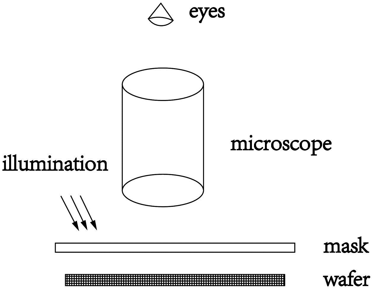
Since the discovery of the moiré phenomenon by Raleigh in 1874[16], it gradually becomes an attractive method for optical alignment. The moiré fringe caused by the interference of light diffracted by the wafer and mask gratings can be seen directly through microscope, as shown in Fig. 1. However, it has difficulty in directly identifying the difference between perfect alignment and sub-period misalignment, which seriously limits its alignment accuracy.
Figure 1.Schematic setup of the alignment system based on the moiré phenomenon.
Two concentric-circle gratings are depicted in Fig. 2, where represents the marks on the mask, and represents the marks on the wafer. Assuming that the transmittance of grating is sinusoidal and can be expressed in terms of polar coordinates as
Figure 2.Analysis of two overlapped concentric-circle gratings.
Similarly, the transmittance of grating is where represents the distance measured from the center of grating . The two-dimensional displacement between grating and grating may be defined by its misalignment magnitude and direction . Then by applying trigonometric rules, we may express as
The misalignment may be assumed to be small enough that is written as
When gratings and are superimposed and illuminated by collimated light, the moiré fringes are obtained, and the transmission function is where the first term is the background contribution, the second and third terms reflect the individual effects of original gratings, the fourth term represents the summing interference that has the radial frequency of (), and the fifth term represents the moiré fringes. Generally, the high frequencies are filtered out, and the phase of moiré fringes is
Moiré fringes show up when , so the solution can be written as where .
Conventional marks are composed of concentric-circle gratings. Assuming that the misalignment between the marks on the wafer and the mask is along the direction, it means , and and are respectively referred to as an actual misalignment and a moiré fringe displacement along the direction. For conventional alignment marks, the actual misalignment ε is magnified by a factor
The moiré fringes generated by conventional concentric-circle marks are shown in Fig. 3. The moiré fringe is a perfect circle when there is no misalignment between the wafer and mask. As the misalignment goes up, the moiré fringe changes as well. However, the moiré fringe changes very little when the misalignment is very small, so that it is difficult to distinguish the moiré pattern between Figs. 3(a) and 3(b), which limits the alignment accuracy.
Figure 3.Conventional moiré fringe generated by a computer (, ) with an direction misalignment of (a) 0, (b) 0.25, (c) 0.5, and (d) 1 μm.
In order to solve the issue above, we propose a novel alignment mark comprising four parts; each part is a quarter of concentric circles with close period or , as shown in Fig. 4.
Figure 4.The designed alignment mark on (a) the mask and (b) the wafer.
Assuming that the misalignment between the marks on the wafer and mask is along direction too, it means the directions in the first and third quadrants are , and the second and fourth quadrants are , . Therefore, the is
The proposed alignment mark doubles the magnification factor, so that a small misalignment between the mask and wafer will bring much more obvious changes in moiré fringes, as shown in Fig. 5.
Figure 5.The designed moiré fringe generated by a computer (, ) with an direction misalignment of (a) 0, (b) 0.2, (c) 0.5, and (d) 1 μm.
When the gratings are misaligned by a 1/10 period of the grating in the direction, an obviously imperfect circle moiré fringe is formed, as shown in Fig. 5(b). As the misalignment increases, the imperfection of the circle becomes more and more obvious. Alignment accuracy of less than a 1/10 grating period is achieved in the experiment.
When the misalignment between the marks on the wafer and mask is along the direction, the directions in the first and third quadrants are , and the directions in the second and fourth quadrants are , . The moiré fringes are similar to Fig. 5, but with a rotation of . When the misalignment is in other direction, it can be decomposed to the direction and the direction, and there is displacement on the moiré fringe of both directions.
There are several advantages of the proposed four-quadrant circle alignment marks. First, high efficiency multi-level elements can be fabricated using conventional UV lithography, which significantly lowers equipment costs. Secondly, the modified marks can significantly enhance the alignment sensitivity. For alignment gratings of a 2 μm period, it is convenient to achieve the alignment accuracy of 0.2 μm. Furthermore, no complicated alignment equipment such as a laser interferometer or software calculation is needed. The moiré fringe can be directly seen through a microscope with broadband illumination when the gap between the wafer and mask changes from 0 to 20 μm. Finally, compared with linear-grating marks, only one set of marks is needed to identify the misalignment in both the and directions, without any extra pre-aligned marks. So, it is very convenient.
The proposed alignment method provides a low-cost, reliable, simple and convenient way for fabricating high efficiency multi-level structures, and the potential capability of the equipment is fully exploited.
In the following section, the fabrication process of four-level membrane optics is briefly introduced.
Considering the flexibility of thin membranes, multi-level surface features were initially made on a fused silica substrate. Then, the liquid polymer was cast onto the substrate and cured in place. Finally, a free-standing patterned membrane was obtained after separation from the substrate.
Figure 6 shows the schematic of the fabrication process. First, four-level FZLs on fused silica were fabricated by twice UV lithography processes; the two masks with the modified alignment marks were made by a laser writer without overlay writing capability. IBE represents ion beam etching. Second, the four-level profile fused silica substrate was cleaned and placed on the rotating platform, and liquid polyimide was cast onto the substrate. Third, the liquid polyimide was allowed to flow for a while to the edge of the substrate, and spin coating was done afterward. Then a second layer of liquid polyimide was cast onto the first layer, and the spin coating was done in the same way. After that, the liquid polyimide and the substrate were placed in a temperature control box for roasting after a 24 h stay in room temperature to minimize the membrane surface fluctuation. Finally, we obtained the patterned replica polyimide membrane after separation from the substrate, as shown in Fig. 7.
Figure 6.Fabrication process of multi-level membrane FZLs.
Reference [17] provides a theoretical description of a continuous phase profile’s discretization. For -level FZLs, the optimal total etched depth can be expressed as[18]where is the refractive index of the polyimide membrane, and is the design wavelength. To avoid the isotropic etch and obtain a perpendicular pattern on the substrate, we choose the ion beam etching over chemical wet etching.
After the second ion beam etching, the alignment error (AE) may cover a previously etched line, and result in spikes at the edge of the third level. These spikes can be removed using a diluted hydrofluoric acid (HF), as shown in Fig. 8.
Figure 8.AFM profiles of four-level FZLs on fused silica before and after HF etching.
In order to test the effect of modified marks, we have done some experiments. Table 1 shows the AE of ten FZLs fabricated on fused silica. Five of them were made by using conventional alignment marks, and the other five FZLs were made by using the modified marks. The AE was measured by an atomic force microscope (AFM).
AE (μm)
Sample 1
Sample 2
Sample 3
Sample 4
Sample 5
Conventional Mark
0.7
0.65
0.65
0.6
0.6
Modified Mark
0.5
0.4
0.4
0.35
0.25
Table 1. Comparison of AE between 5 FZLs Fabricated on Fused Silica by Using Conventional Alignment Marks and Modified Alignment Marks, (p1=4.2 μm, p2=4 μm)
According to the test results, the average AE of the FZLs made by conventional alignment marks is 0.64 μm. By using the modified alignment marks, the average AE is significantly reduced to 0.38 μm, as shown in Table 1. Many factors affect the final results, such as the line width error and the manual error. More experiments are required to achieve a stable performance.
Furthermore, the diffraction efficiency into the order of FZLs was measured. The average efficiency of FZLs made by conventional marks is 45.5%. With the modified marks, the efficiency average of FZLs is 59.02%, as shown in Table 2. The diffraction efficiency is significantly improved by 13.52% only with the modified alignment marks.
Diffraction Efficiency
Sample 1 (%)
Sample 2 (%)
Sample 3 (%)
Sample 4 (%)
Sample 5 (%)
Conventional Mark
42.5
45
45
47
48
Modified Mark
54
55
58
61.5
66.6
Table 2. Comparison of Diffraction Efficiency between 5 FZLs Fabricated on Fused Silica by Using Conventional Alignment Marks and Modified Alignment Marks, (p1=4.2 μm, p2=4 μm)
Based on the proposed method, a four-level membrane FZL in 200 mm diameters was made. The full-aperture diffraction efficiency is 62.5%, and the root mean square (RMS) efficiency is 0.051, as shown in Fig. 9.
Figure 9.Diffraction efficiency of a four-level membrane FZL.
The transmittance of the polyimide membrane is 85%, so the theoretical efficiency at the order is 68.85%.
We use the AFM to measure the profiles of the FZLs and analyze the data using the software “PC Grate”.
According to Eq. (12), the ideal total etching depth is 660 nm. However, the AFM test shows that the actual etching depth is about 740 nm, which decreases the diffraction efficiency about 4%. The duty cycle of the FZLs’ grating ranges from 0.55 to 0.6, which decreases the efficiency about 1.4%, and the AE decreases the efficiency about 0.95%. The data implies that the etching depth and line width errors can be reduced, and the AE is relatively well controlled.
In this Letter, a modified alignment method based on an improved moiré technique is demonstrated to realize highly accurate and reliable alignment of multi-level FZLs on fused silica by using conventional UV lithography. Compared to conventional alignment marks, the AE is reduced and the diffraction efficiency is significantly improved by 13.52%. As an alternative of the laser overlay writing method, the modified alignment method through novel designed marks shows the potential to reduce the cost and achieve a high accuracy.
Replication of fused silica four-level patterns in 200 mm diameter and 20 μm thick membranes is demonstrated, with an over 62% diffraction efficiency into the order and the RMS efficiency of 0.051. Wavefront control, pattern expansion, and in-plane stress responses of membrane optics require further work to be understood. This work can provide a reference for future large-aperture ultralight space telescopes.