• Chinese Optics Letters
  • Vol. 13, Issue 10, 102401 (2015)
Zhaoxu Yan1、2, Chunhao Li1, Yang Luo3, Jihong Zhao1、*, Hai Yang4, Prabhat Verma2, and Satoshi Kawata 2、**
Author Affiliations
  • 1State Key Laboratory on Integrated Optoelectronics, College of Electronic Science and Engineering, Jilin University, Changchun 130012, China
  • 2Department of Applied Physics, Osaka University, 2-1 Yamadaoka, Suita, Osaka 565-0871, Japan
  • 3Changchun Institute of Optics, Fine Mechanics and Physics, Chinese Academy of Sciences, Changchun 130033, China
  • 4General Research Institute for Nonferrous Metals, Beijing 100088, China
  • show less
    DOI: 10.3788/COL201513.102401 Cite this Article Set citation alerts
    Zhaoxu Yan, Chunhao Li, Yang Luo, Jihong Zhao, Hai Yang, Prabhat Verma, Satoshi Kawata . Silver hierarchical structures grown on microstructured silicon in chip for microfluidic integrated catalyst and SERS detector[J]. Chinese Optics Letters, 2015, 13(10): 102401 Copy Citation Text show less
    Schematic illustration of the experiment. (I–III) Microfluidic chip fabrication on Si wafer by dry etching. (IV–V) BS fabrication by laser. (VI) HF treatment on BS. (VII) AgNPs’ growth on BS. (VIII) Catalytic reaction and SERS detection on Ag-BS substrate.
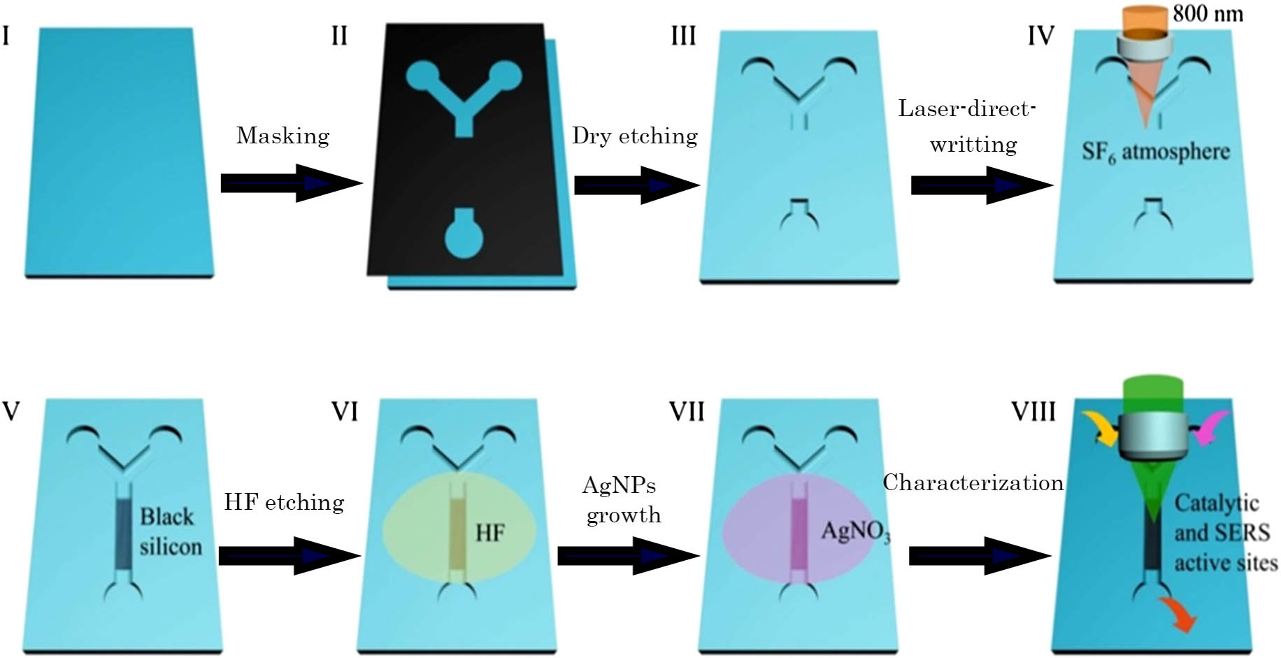
    Fig. 1. Schematic illustration of the experiment. (I–III) Microfluidic chip fabrication on Si wafer by dry etching. (IV–V) BS fabrication by laser. (VI) HF treatment on BS. (VII) AgNPs’ growth on BS. (VIII) Catalytic reaction and SERS detection on Ag-BS substrate.
    SEM images of the BS with (a) side view and (b) oblique view.
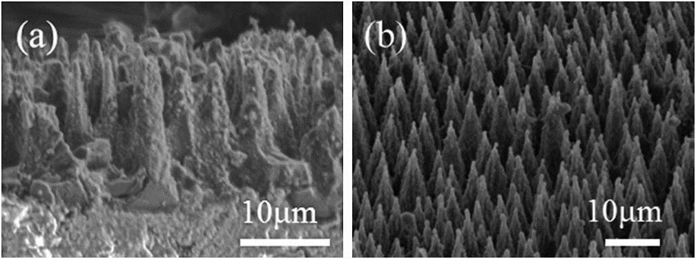
    Fig. 2. SEM images of the BS with (a) side view and (b) oblique view.
    (a) SEM image of the AgNPs on the BS protrusions. (b), (c), and (d) Enlarged SEM images of AgNPs on the area marked by red, green, and blue squares in (a).
    Fig. 3. (a) SEM image of the AgNPs on the BS protrusions. (b), (c), and (d) Enlarged SEM images of AgNPs on the area marked by red, green, and blue squares in (a).
    SEM images of the AgNPs grown under (a) 15°C, (b) 25°C, (c) 50°C, and (d) 75°C. The scale bars indicate 100 nm.
    Fig. 4. SEM images of the AgNPs grown under (a) 15°C, (b) 25°C, (c) 50°C, and (d) 75°C. The scale bars indicate 100 nm.
    SEM images of the AgNPs grown in (a) 0.001, (b) 0.01, (c) 0.1, and (d) 1 mol/L AgNO3 solution. The scale bars indicate 100 nm.
    Fig. 5. SEM images of the AgNPs grown in (a) 0.001, (b) 0.01, (c) 0.1, and (d) 1 mol/L AgNO3 solution. The scale bars indicate 100 nm.
    EDS spectra of the Ag-BS (a) under different reaction temperatures, where inset shows the peak intensity versus temperature; and (b) with different AgNO3 solution concentrations, where inset shows the peak intensity versus concentration.
    Fig. 6. EDS spectra of the Ag-BS (a) under different reaction temperatures, where inset shows the peak intensity versus temperature; and (b) with different AgNO3 solution concentrations, where inset shows the peak intensity versus concentration.
    SERS spectra taken before (black line) and after (red line) the catalytic reaction of pNP to pAP. Inset illustrates the chemical reaction process.
    Fig. 7. SERS spectra taken before (black line) and after (red line) the catalytic reaction of pNP to pAP. Inset illustrates the chemical reaction process.
    SERS spectra of R6G with the concentrations ranging from 10−6 to 10−8 M.
    Fig. 8. SERS spectra of R6G with the concentrations ranging from 106 to 108M.
    Zhaoxu Yan, Chunhao Li, Yang Luo, Jihong Zhao, Hai Yang, Prabhat Verma, Satoshi Kawata . Silver hierarchical structures grown on microstructured silicon in chip for microfluidic integrated catalyst and SERS detector[J]. Chinese Optics Letters, 2015, 13(10): 102401
    Download Citation