• Journal of Infrared and Millimeter Waves
  • Vol. 40, Issue 3, 314 (2021)
Yue LU1, Hao XU2, Xiao-Wen LI2, Fang PENG2, Yan SUN2、*, Ding WANG1、**, and Jiao-Ming HAO2
Author Affiliations
  • 1School of Materials Science and Engineering, University of Shanghai for Science and Technology, Shanghai 200093, China
  • 2State Key Laboratory of Infrared Physics, Shanghai Institute of Technical Physics, Chinese Academy of Sciences, Shanghai 200083, China
  • show less
    DOI: 10.11972/j.issn.1001-9014.2021.03.006 Cite this Article
    Yue LU, Hao XU, Xiao-Wen LI, Fang PENG, Yan SUN, Ding WANG, Jiao-Ming HAO. Visible-near infrared light superabsorption of aluminum-based planar metamaterial[J]. Journal of Infrared and Millimeter Waves, 2021, 40(3): 314 Copy Citation Text show less
    Preparation flowchart of aluminum-based electromagnetic absorber(a) Silicon substrate,(b) Silicon substrate/aluminum film,(c) Silicon substrate/aluminum/alumina film,(d) Silicon substrate/aluminum/alumina/aluminum film
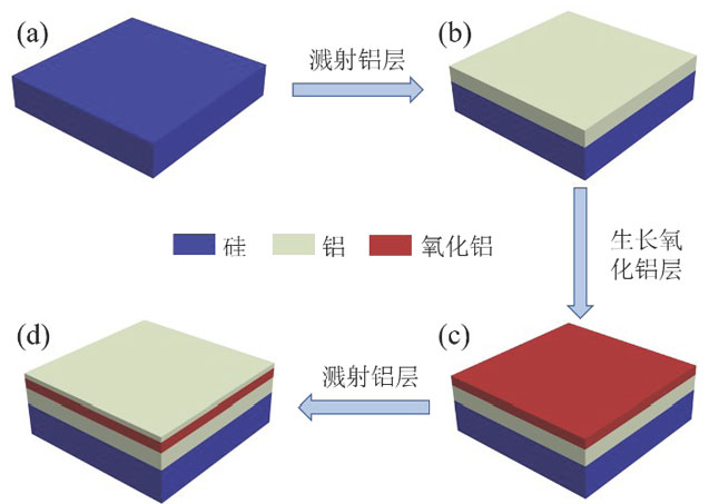
    Fig. 1. Preparation flowchart of aluminum-based electromagnetic absorber(a) Silicon substrate,(b) Silicon substrate/aluminum film,(c) Silicon substrate/aluminum/alumina film,(d) Silicon substrate/aluminum/alumina/aluminum film
    An absorber with a three-layer film stack structure(a) Schematic structure,(b) SEM cross-sectional view
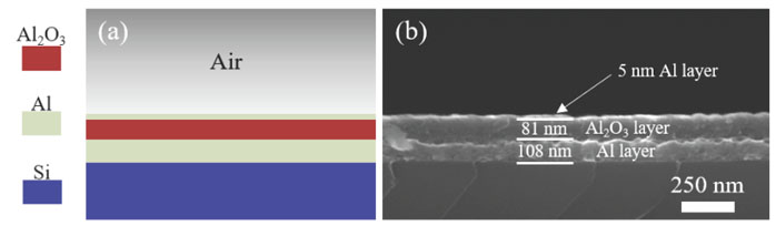
    Fig. 2. An absorber with a three-layer film stack structure(a) Schematic structure,(b) SEM cross-sectional view
    Reflectance spectrum curves of the absorber(a) The experimental reflection spectrum curve of samples with alumina thickness of 63 nm, 73 nm, 81 nm, and 90 nm,(b) The simulation of samples with alumina thickness of 63 nm, 73 nm, 81 nm, and 90 nm. Reflection spectrum curve,(c) The experimental reflection spectrum curve of samples with alumina thickness of 105 nm, 117 nm, 136 nm and 146 nm,(d) The simulated reflection spectrum curve of samples with alumina thickness of 105 nm, 117 nm, 136 nm and 146 nm
    Fig. 3. Reflectance spectrum curves of the absorber(a) The experimental reflection spectrum curve of samples with alumina thickness of 63 nm, 73 nm, 81 nm, and 90 nm,(b) The simulation of samples with alumina thickness of 63 nm, 73 nm, 81 nm, and 90 nm. Reflection spectrum curve,(c) The experimental reflection spectrum curve of samples with alumina thickness of 105 nm, 117 nm, 136 nm and 146 nm,(d) The simulated reflection spectrum curve of samples with alumina thickness of 105 nm, 117 nm, 136 nm and 146 nm
    Schematic diagram of absorber structure
    Fig. 4. Schematic diagram of absorber structure
    Optical parameters of each layer of 100 nm Al/63 nm Al2O3/5 nm Al(a) 100 nm aluminum,(b) 63 nm Alumina,(c) 5 nm aluminum. The black curve is the refractive index n, and the red curve is the extinction coefficient k
    Fig. 5. Optical parameters of each layer of 100 nm Al/63 nm Al2O3/5 nm Al(a) 100 nm aluminum,(b) 63 nm Alumina,(c) 5 nm aluminum. The black curve is the refractive index n, and the red curve is the extinction coefficient k
    Line chart of the thickness relationship between the superabsorber cavity and the position of the absorption peak
    Fig. 6. Line chart of the thickness relationship between the superabsorber cavity and the position of the absorption peak
    Variable angle reflection spectra of the device under different polarization states. Experimental(a-c) and calculated(d-f) reflectance spectra as a function of incidence angles under different polarization conditions
    Fig. 7. Variable angle reflection spectra of the device under different polarization states. Experimental(a-c) and calculated(d-f) reflectance spectra as a function of incidence angles under different polarization conditions
    The electric and magnetic field distribution at the resonant wavelength of the sample at 8° incidence(a) The electric field distribution at the xz longitudinal section(y=0 nm),(b) The magnetic field distribution at the xz longitudinal section(y=0 nm)
    Fig. 8. The electric and magnetic field distribution at the resonant wavelength of the sample at 8° incidence(a) The electric field distribution at the xz longitudinal section(y=0 nm),(b) The magnetic field distribution at the xz longitudinal section(y=0 nm)
    (a) Diagram of the experimental setup of the electromagnetic absorber for light heating,(b) The heating curve of the sample under 240 mW laser power,(c) The heating curve of the sample under 300 mW laser power,(d) The heating curve of the sample under 440 mW laser power, in which the black curve is the room temperature change curve, and the red curve is the sample temperature change curve
    Fig. 9. (a) Diagram of the experimental setup of the electromagnetic absorber for light heating,(b) The heating curve of the sample under 240 mW laser power,(c) The heating curve of the sample under 300 mW laser power,(d) The heating curve of the sample under 440 mW laser power, in which the black curve is the room temperature change curve, and the red curve is the sample temperature change curve
    氧化铝厚度/nm超吸收峰位/nm吸收带宽/nm超吸收范围/nm
    63504231417~648
    73567246474~720
    80630279525~804
    90687312573~885
    105891432717~1 149
    117963462777~1 239
    1361 098537894~1 431
    1461 176540960~1 500
    Table 1. The relationship between the thickness of alumina and the peak position, bandwidth and range of the devices’ superabsorption
    Yue LU, Hao XU, Xiao-Wen LI, Fang PENG, Yan SUN, Ding WANG, Jiao-Ming HAO. Visible-near infrared light superabsorption of aluminum-based planar metamaterial[J]. Journal of Infrared and Millimeter Waves, 2021, 40(3): 314
    Download Citation