• Chinese Physics B
  • Vol. 29, Issue 9, (2020)
Xing-Yu Zhang1、2, Yong-Liang Wang1、3、†, Chao-Lin Lv1、3, Li-Xing You1、2、3, Hao Li1、3, Zhen Wang1、3, and Xiao-Ming Xie1、3
Author Affiliations
  • 1State Key Laboratory of Functional Material for Informatics, Shanghai Institute of Microsystem and Information Technology, Chinese Academy of Sciences (CAS), Shanghai 200050, China
  • 2Center of Materials Science and Optoelectronics Engineering, University of Chinese Academy of Sciences, Beijing 100049, China
  • 3CAS Center for Excellence in Superconducting Electronics, Shanghai 200050, China
  • show less
    DOI: 10.1088/1674-1056/ab90f4 Cite this Article
    Xing-Yu Zhang, Yong-Liang Wang, Chao-Lin Lv, Li-Xing You, Hao Li, Zhen Wang, Xiao-Ming Xie. Flux-to-voltage characteristic simulation of superconducting nanowire interference device[J]. Chinese Physics B, 2020, 29(9): Copy Citation Text show less
    (a) Three states of nanowire: (i) superconducting state, (ii) hotspot state, (iii) normal state (“latched” state). ψ1,2 denotes the wave function at both ends of the nanowire. (b) Schematic diagram of simplified nanowire model. L1 denotes the inductance of nanowire. Rhs represents the resistance of hotspot region in hotspot state. SW refers to the switching effect of nanowires. SW is open for hotspot state, while closed for superconducting state.
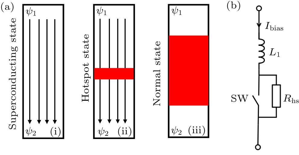
    Fig. 1. (a) Three states of nanowire: (i) superconducting state, (ii) hotspot state, (iii) normal state (“latched” state). ψ1,2 denotes the wave function at both ends of the nanowire. (b) Schematic diagram of simplified nanowire model. L1 denotes the inductance of nanowire. Rhs represents the resistance of hotspot region in hotspot state. SW refers to the switching effect of nanowires. SW is open for hotspot state, while closed for superconducting state.
    (a) Schematic diagram of two parallel ultrathin superconducting nanowires. Ibias is the current through parallel nanowires, i1,2 denote the currents in nanowires, and iflux represents the circulating current due to external magnetic flux Φe. The direction of circulation depends on fluxoid number n. (b) Equivalent circuit of parallel nanowires based on switch model. L1,2 denotes nanowire’s inductance. SW1,2 represents the switching effect of the nanowire. SW1,2 is open for hotspot state with hotspot resistance Rhs, while closed for superconducting state. (c) Simulation results of flux-to-voltage conversion curves in parallel nanowires. The bias currents for different curves increase from 1.3 ⋅ Isw to 2.5 ⋅ Isw in steps of 0.2 ⋅ Isw from bottom to top. Modulation disappears due to the latching effect.
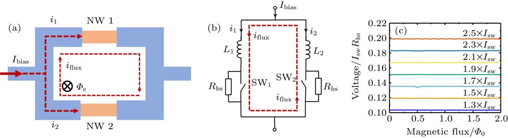
    Fig. 2. (a) Schematic diagram of two parallel ultrathin superconducting nanowires. Ibias is the current through parallel nanowires, i1,2 denote the currents in nanowires, and iflux represents the circulating current due to external magnetic flux Φe. The direction of circulation depends on fluxoid number n. (b) Equivalent circuit of parallel nanowires based on switch model. L1,2 denotes nanowire’s inductance. SW1,2 represents the switching effect of the nanowire. SW1,2 is open for hotspot state with hotspot resistance Rhs, while closed for superconducting state. (c) Simulation results of flux-to-voltage conversion curves in parallel nanowires. The bias currents for different curves increase from 1.3 ⋅ Isw to 2.5 ⋅ Isw in steps of 0.2 ⋅ Isw from bottom to top. Modulation disappears due to the latching effect.
    (a) Schematic diagram of the nanowire interference device with a shunt resistor. It comprises two parallel ultrathin superconducting nanowires shunted with resistor Rshunt. External inductance Lshunt is taken into consideration to estimate the effect of parasitic parameters. Φe is the external magnetic flux applied to the device. i1,2,3 denote the currents through the parallel nanowires and the shunt resistor respectively. (b) Equivalent circuit of the device with a shunt resistor. Φe is the external magnetic flux applied to the device. L1,2 denote the inductances of nanowires. SW1,2 denote the switching effect of nanowires. SW1,2 is open for hotspot state with hotspot resistance of Rhs, while it is closed for the superconducting state.
    Fig. 3. (a) Schematic diagram of the nanowire interference device with a shunt resistor. It comprises two parallel ultrathin superconducting nanowires shunted with resistor Rshunt. External inductance Lshunt is taken into consideration to estimate the effect of parasitic parameters. Φe is the external magnetic flux applied to the device. i1,2,3 denote the currents through the parallel nanowires and the shunt resistor respectively. (b) Equivalent circuit of the device with a shunt resistor. Φe is the external magnetic flux applied to the device. L1,2 denote the inductances of nanowires. SW1,2 denote the switching effect of nanowires. SW1,2 is open for hotspot state with hotspot resistance of Rhs, while it is closed for the superconducting state.
    (a) Simulation results of current–voltage characteristic with a shunt resistor. Bias current is normalized by switching current of single nanowire Isw, and output voltage is normalized by the multiplication of switching current and shunt resistance. (b) Simulation results of flux-to-voltage conversion curves. Bias currents of flux modulation curves increase from 1.1 ⋅ Isw to 2.5 ⋅ Isw in steps of 0.2 ⋅ Isw from bottom to top. Each curve has periodicity and symmetry.
    Fig. 4. (a) Simulation results of current–voltage characteristic with a shunt resistor. Bias current is normalized by switching current of single nanowire Isw, and output voltage is normalized by the multiplication of switching current and shunt resistance. (b) Simulation results of flux-to-voltage conversion curves. Bias currents of flux modulation curves increase from 1.1 ⋅ Isw to 2.5 ⋅ Isw in steps of 0.2 ⋅ Isw from bottom to top. Each curve has periodicity and symmetry.
    Flux-to-voltage conversion curves for devices with different values of shunt resistance and nanowire inductance. (a) Curves for different values of shunt resistance. Shunt resistances are selected to be 0.01 ⋅ Rhs, 0.05 ⋅ Rhs, 0.1 ⋅ Rhs, 0.15 ⋅ Rhs, and 0.25 ⋅ Rhs respectively from bottom to top for Ibias = 2 ⋅ Isw. Output voltage is normalized by the multiplication of switching current and hotspot resistance. For a smaller resistor, device can support higher bias current, but output voltage is lower. When resistance becomes larger, device is easier to latch. (b) Flux-to-voltage conversion curves for different values of nanowire inductance of 16.5, 66, 100, 165, 230 pH, respectively, for Ibias = 2 Φ Isw. Output voltage is normalized by the multiplication of switching current and shunt resistance. As the inductance of nanowire decreases, modulation curve becomes steeper, while output voltage slightly increases.
    Fig. 5. Flux-to-voltage conversion curves for devices with different values of shunt resistance and nanowire inductance. (a) Curves for different values of shunt resistance. Shunt resistances are selected to be 0.01 ⋅ Rhs, 0.05 ⋅ Rhs, 0.1 ⋅ Rhs, 0.15 ⋅ Rhs, and 0.25 ⋅ Rhs respectively from bottom to top for Ibias = 2 ⋅ Isw. Output voltage is normalized by the multiplication of switching current and hotspot resistance. For a smaller resistor, device can support higher bias current, but output voltage is lower. When resistance becomes larger, device is easier to latch. (b) Flux-to-voltage conversion curves for different values of nanowire inductance of 16.5, 66, 100, 165, 230 pH, respectively, for Ibias = 2 Φ Isw. Output voltage is normalized by the multiplication of switching current and shunt resistance. As the inductance of nanowire decreases, modulation curve becomes steeper, while output voltage slightly increases.
    VariableParameterSimulation value
    L1,2inductance of nanowires160 pH
    Iswswitching current of nanowires10 μA
    Rhsresistance of nanowires/
    Rshuntshunt resistance0.03 ⋅ Rhs
    Lshuntshunt inductance∼ 10 pH
    Table 1. Simulation parameters for device.
    Xing-Yu Zhang, Yong-Liang Wang, Chao-Lin Lv, Li-Xing You, Hao Li, Zhen Wang, Xiao-Ming Xie. Flux-to-voltage characteristic simulation of superconducting nanowire interference device[J]. Chinese Physics B, 2020, 29(9):
    Download Citation