
Kyung Rock Son, Byeong Ryong Lee, Min Ho Jang, Hyun Chul Park, Yong Hoon Cho, Tae Geun Kim, "Enhanced light emission from AlGaN/GaN multiple quantum wells using the localized surface plasmon effect by aluminum nanoring patterns," Photonics Res. 6, 30 (2018)
- Photonics Research
- Vol. 6, Issue 1, 30 (2018)
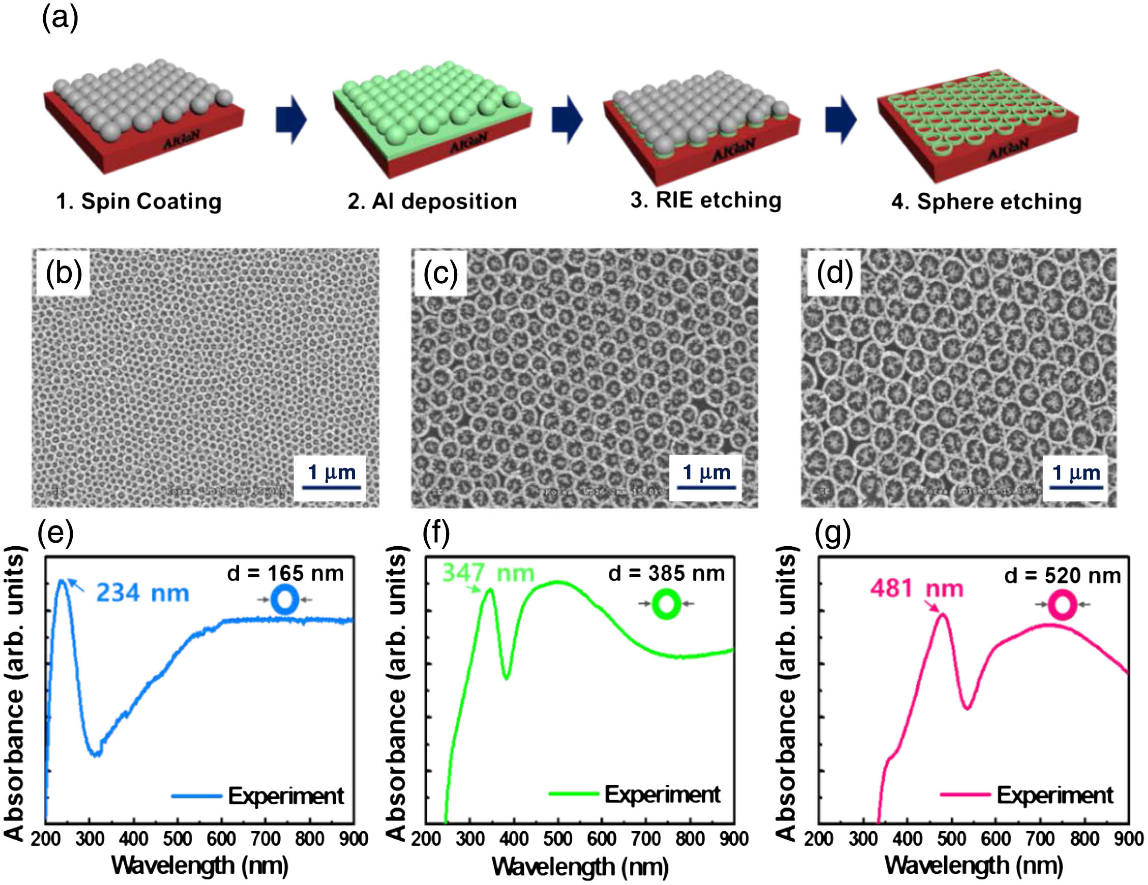
Fig. 1. (a) Schematics of the processing steps used to fabricate Al nanoring arrays using SiO 2 SiO 2
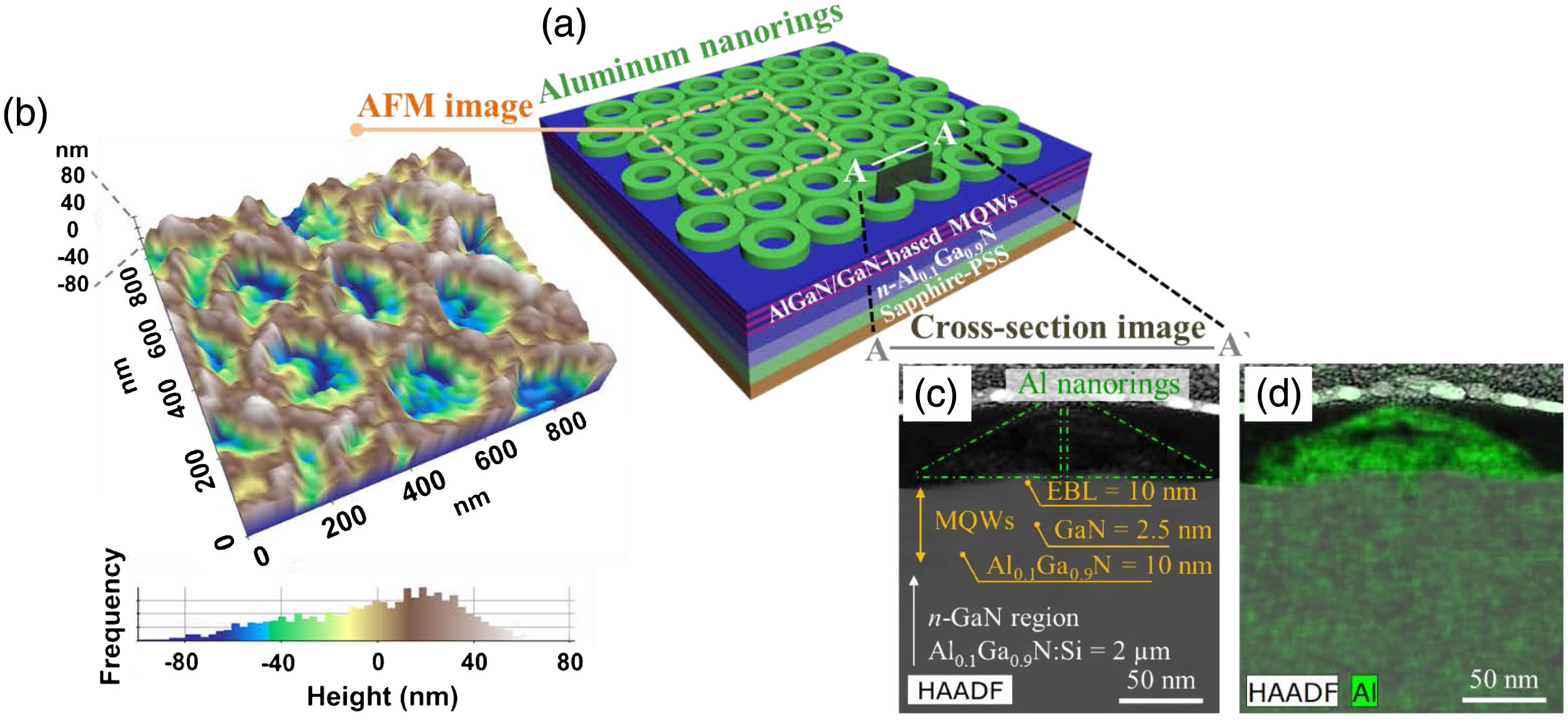
Fig. 2. (a) Schematic of the AlGaN/GaN-based near-UV LED structure with Al nanorings to capture both AFM and TEM images. (b) AFM image of the top surface of the near-UV LED with 385 nm Al nanorings that have an HCP array structure and height distribution. (c) STEM cross-sectional image of the AlGaN/GaN-based near-UV LED with Al nanorings and (d) the corresponding EDS mapping image of Al element (green color).
Fig. 3. 3D FDTD simulations of the Al nanoring array, which has an HCP structure with outer diameters of 385 nm, plasmonic system. (a) Schematic of the simulated Al nanoring array–HCP unit cell structure. (b) Simulated absorbance spectra of the Al nanoring array with an HCP unit cell on the glass substrate, when the incident light was both TE and TM polarized. Top views of the local electric field distributions of Al nanorings with HCP unit cell on the Al 0.1 Ga 0.9 N z = 0 nm z = − 16 nm
Fig. 4. (a) Power-dependent PL measurements with source power of 0.03, 0.1, 0.5, 2, and 8 mW from bottom to top. (b) Time-resolved PL spectra of the AlGaN/GaN MQW structure with and without Al nanorings at room temperature.
Fig. 5. (a) Temporal evolution of MQW emissions obtained at different temperatures for AlGaN/GaN MQW samples with and without Al nanoring structures. For both samples, temporal curves are normalized and vertically shifted for comparison. Measured PL lifetime τ m τ r τ n r
Fig. 6. TDPL measurements. PL spectra of AlGaN/GaN MQW structures (a) without Al nanorings (b) with Al nanorings at temperatures from 12 to 300 K. (c) Arrhenius plot of the normalized integrated PL intensities for AlGaN/GaN MQWs with and without Al nanorings.


Set citation alerts for the article
Please enter your email address

© Copyright 2018-2021 | Chinese Laser Press. All Rights Reserved 沪ICP备15018463号-20