• Laser & Optoelectronics Progress
  • Vol. 55, Issue 2, 020006 (2018)
Yuewu Yan1、2, Junming An1、2, Jiashun Zhang、*, Liangliang Wang1, Xiaojie Yin1, Yuanda Wu1、2, and Yue Wang1
Author Affiliations
  • 1 State Key Laboratory on Integrated Optoelectronics, Institute of Semiconductors, Chinese Academy of Sciences, Beijing 100083, China
  • 2 College of Materials Science and Opto-Electronic Technology, University of Chinese Academy of Sciences, Beijing 100049, China
  • show less
    DOI: 10.3788/LOP55.020006 Cite this Article Set citation alerts
    Yuewu Yan, Junming An, Jiashun Zhang, Liangliang Wang, Xiaojie Yin, Yuanda Wu, Yue Wang. Research Progress of Optical Phased Array Technology[J]. Laser & Optoelectronics Progress, 2018, 55(2): 020006 Copy Citation Text show less
    Schematic of optical phased array
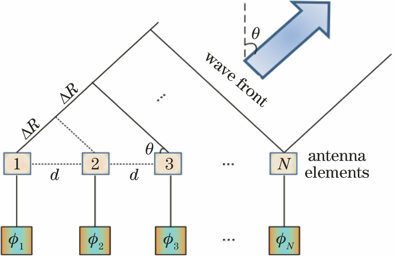
    Fig. 1. Schematic of optical phased array
    Schematic of the beam scanner in Ref. [16]
    Fig. 2. Schematic of the beam scanner in Ref. [16]
    Ten waveguide optical phased array
    Fig. 3. Ten waveguide optical phased array
    Schematic of the beam scanning component
    Fig. 4. Schematic of the beam scanning component
    Schematic of the 16-channel grating array. (a) Device structure; (b) angle alignment of longitudinal axis and transverse axis
    Fig. 5. Schematic of the 16-channel grating array. (a) Device structure; (b) angle alignment of longitudinal axis and transverse axis
    Device structure and simulation. (a) Schematic of the silicon waveguide based optical phased array; (b) beam propagation simulation
    Fig. 6. Device structure and simulation. (a) Schematic of the silicon waveguide based optical phased array; (b) beam propagation simulation
    Nanophotonic phased array system
    Fig. 7. Nanophotonic phased array system
    Device structure and SEM scanning graphs. (a) 3D rendering of the optical phased array; SEM graphs of (b) cascaded phase shifter architecture, (c) close-up of the thermal phase shifters, (d) full-etch silicon grating based antennas
    Fig. 8. Device structure and SEM scanning graphs. (a) 3D rendering of the optical phased array; SEM graphs of (b) cascaded phase shifter architecture, (c) close-up of the thermal phase shifters, (d) full-etch silicon grating based antennas
    Schematic of the phased array antenna[35]
    Fig. 9. Schematic of the phased array antenna[35]
    Schematic of optical phased array composed of HCG mirrors
    Fig. 10. Schematic of optical phased array composed of HCG mirrors
    Schematic of MEMS phased array composed of HCG
    Fig. 11. Schematic of MEMS phased array composed of HCG
    Schematic of phased array lidar
    Fig. 12. Schematic of phased array lidar
    TypeSteeringspeed /kHzControlvoltage /VSteeringangle /(°)Integration
    LC5[43]6.882Low
    Waveguide100[20]1051High
    MEMS632[42]102High
    Table 1. Comparison of three kinds of optical phased array
    Yuewu Yan, Junming An, Jiashun Zhang, Liangliang Wang, Xiaojie Yin, Yuanda Wu, Yue Wang. Research Progress of Optical Phased Array Technology[J]. Laser & Optoelectronics Progress, 2018, 55(2): 020006
    Download Citation