
Shivendra Yadav, Alish Pamnani, Dheeraj Sharma, Anju Gedam, Atul Kumar, Neeraj Sharma. A novel design approach of charge plasma tunnel FET for radio frequency applications[J]. Journal of Semiconductors, 2019, 40(5): 052901
- Journal of Semiconductors
- Vol. 40, Issue 5, 052901 (2019)
Abstract
1. Introduction
With the advent of MOSFET, technology over the past few decades has reached to new heights. The dimensions of MOSFET in the last decade has been reduced by three orders of magnitude in order to attain high performance integrated circuits[
According to international technology roadmap for semiconductors (ITRS) 2005, to overcome these critical issues, tunnel FET (TFET) has proved itself to be a best alternative of MOSFET[
Physically doped TFET suffers from random dopant fluctuations (RDFs) at nano scale regim. RDFS is defined as movement of dopant atoms across the junction and it has sever effects on TFET as compared to MOSFET[
In this concern, EES is deposited below the source/ channel junction of the CP-TFET which improves its DC and RF performances. This leads to the formation of new device double source charge plasma TFET (DS-CP-TFET). But, this device faces the problem of static power dissipation and negative conductance[
2. Device structure and simulation
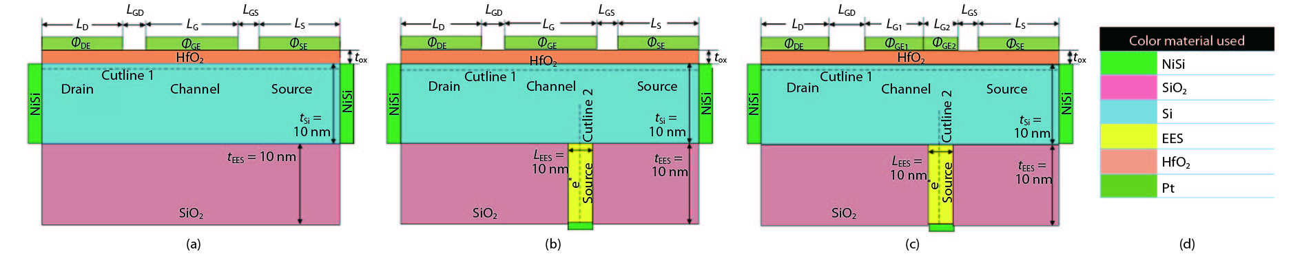
Figs. 1(a)–1(c) depicts the cross sectional view of device CP-TFET, DS-CP-TFET and DS-DG-CP-TFET. Fig. 1(d) shows the color bar of materials used in different color regions. A lightly doped silicon layer of concentration 1015 cm–3 is used for the substrate for all the three devices. The metal electrode of different WF 3.4 eV (Hf) and 5.93 eV (Pt) is used to form n+ and p+ region respectively[
![]()
Figure 1.(Color online) Cross sectional view (a) CP-TFET, (b) DS-CP-TFET, (c) DS-DG-CP-TFET, and (d) color bar of materials.
For all three devices, length of source electrode (
3. Results and discussion
This section describes relative comparison of performances among three devices i.e. CP-TFET, DS-CP-TFET and DS-DG-CP-TFET in terms of their DC characteristics and Analog/RF parameters.
3.1. DC characteristics
Conventional physically doped TFET has ON state current in nano ampere range and OFF state current in femto ampere range at
![]()
Figure 2.(Color online) (a) Carrier concentration of DS-DG-CP-TFET as reported in Refs. [
Electric field distribution along the channel is shown in Fig. 3(a). All the three devices have the same peak which shows that the tunneling probability is almost same for all the three devices. This is further supported by Fig. 3(b), which shows the energy band diagram (EBD) along cutline 1. Fig. 3(b) shows almost similar tunneling width for all three devices. Both of these observations clearly indicate that the increase in ON state current in DS-CP-TFET and DS-DG-CP-TFET is due to EES placed below the channel. Fig. 4(a) shows the EBD in ON state along cutline 2 and it can be observed that the electrons move from the EES to the channel over the barrier through thermionic emission. When the positive gate and drain voltage is applied on device a resultant positive voltage exist over the EES and other end of EES is connected with ground source. Since, EES is heavily doped so electrons came out easily from EES into the channel region through over the barrier. This is also evident from Fig. 4(b) in which the electron current density in ON state has been investigated by contour plot which indicates that additional current density is provided by the EES. Therefore, there is significant increase in ON state current in case of DS-CP-TFET and DS-DG-CP-TFET which can be seen from Fig. 5(a). From Fig. 5(a), it can also be observed that DS-CP-TFET has high leakage current. This has been rectified by employing dual metal gate engineering in DS-DG-CP-TFET. Fig. 5(b) shows EBD in OFF state along cutline 1 and it can be seen that there is an uplift in the energy band under GE1 causes the formation of potential well and restricts the movement of leaky charge carriers in the channel. Apart from this Fig. 6(a) indicates EBD in ambipolar state, where drain underlapping in DS-DG-CP-TFET clearly illustrates that tunneling width is getting wider as compared to other two devices. The advantageous impact of wider tunneling width at drain/channel junction can be visualized in terms of suppressed ambipolar current in proposed structure in Fig. 6(b). The figure is showing distribution of drain current for negative gate voltage in comparative manner in ambipolar state.
![]()
Figure 3.(Color online) (a) Electrical field and (b) EBD along cutline 1 in ON state.
![]()
Figure 4.(Color online) (a) EBD along cutline 2 and (b) contour plot of current density in ON state.
![]()
Figure 5.(Color online) Variation of (a) TC in ON state and (b) EBD along cutline 1 in ambipolar state.
![]()
Figure 6.(Color online) Variation of (a) EBD along cutline 1 in OFF state and (b) TC in ambipolar state.
A relative study of DC characteristics is shown in Table 1. In the table, reported values of
![]()
Figure 7.(Color online) (a)
3.2. RF analysis
In the present-day framework, RF figures of merit are critical parameters for determining the performance of the device. For elucidating analog performances of device there are various fundamental characteristics such as transconductance (
Transconductance (
![]()
Figure 8.(Color online) Variation of (a)
Cut-off frequency
![]()
Figure 9.(Color online) Variation of (a)
![]()
Figure 10.(Color online) Variation of IG with
It can be seen from Fig. 11(a) that
![]()
Figure 11.(Color online) Variation of (a)
4. Optimisation
In this section, we are trying to select the appropriate values of
![]()
Figure 12.(Color online) (a) TC and (b)
Dual metal gate engineering is used in DS-DG-CP-TFET to reduce the leakage current. Fig. 13(a) shows the TC for different value of
![]()
Figure 13.(Color online) (a) TC of DS-DG-CP-TFET for different WF of GE1 and (b) variation in cutoff frequency with
Supression of negative conductance is very important in circuit level performances. TC for different values of
![]()
Figure 14.(Color online) (a) TC of DS-DG-CP-TFET for different spacer length (
5. Conclusion
CP-TFET has low ON state current and poor RF performance. To resolve these issues DS-CP-TFET has been formed to increase ON state current by using EES but on the other hand it has issue of ambipolarity and leakage current. Therefore, a novel device DS-DG-CP-TFET has been proposed which improves device performance in terms of DC and Analog/RF parameters. It uses EES for increasing ON state current, dual metal gate engineering for lowering leakage current and drain underlapping technique for reducing ambipolarity. Further, optimizations are done in the position of EES, WF of GE1 and
References
[1] R H Dennard, F H Gaensslen, H N Yu et al. Design of ion-implanted MOSFET's with very small physical dimensions. IEEE J Solid-State Circuits, 87, 668(1999).
[2] K Gopalakrishnan, R Woo, C Jungemann et al. Impact ionization MOS (I-MOS)-Part II: Experimental results. IEEE Trans Electron Devices, 52, 77(2005).
[3] R Hajare, C Lakshminarayana, G H Raghunandan et al. Performance enhancement of FINFET and CNTFET at different node technologies. Microsyst Technol, 22, 1121(2016).
[4]
[5] S O Koswatta, M S Lundstrom, D E Nikonov. Performance comparison between p-i-n tunneling transistors and conventional MOSFETs. IEEE Trans Electron Devices, 56, 456(2009).
[6] N damrongplasit, S H Kim, T J K Liu. Study of random dopant fluctuation induced variability in the raised-Ge source TFET. IEEE Electron Device Lett, 34, 184(2013).
[7] N damrongplasit, C Shin, S H Kim et al. Study of random dopant fluctuation effects in germanium-source tunnel FETs. IEEE Trans Electron Devices, 58, 3541(2011).
[8] R Jhaveri, V Nagavarapu, J C S Woo. Effect of pocket doping and annealing schemes on the source-pocket tunnel field-effect transistor. IEEE Trans Electron Devices, 58, 80(2011).
[9] M J Kumar, K Nadda. Bipolar charge-plasma transistor:a novel three terminal device. IEEE Trans Electron Devices, 59, 962(2012).
[10] H Kroemer. Negative conductance in semiconductors. IEEE Spectrum, 5, 47(1968).
[11] S Yadav, D Sharma, B V Chandan et al. A novel hetero-material gate-underlap electrically doped TFET for improving DC/RF and ambipolar behaviour. Superlattices Microstruct, 117, 9(2018).
[12]
[13] T Aaltonen, M Ritala, T Sajavaara et al. Atomic layer deposition of platinum thin films. Chem Mater, 15, 1924(2018).
[14] F Gossenberger, T Roman, K F Tonigold et al. Change of the work function of platinum electrodes induced by halide adsorption. Beilst J Nanotechnol, 5, 152(2014).
[15] B Rajasekharan, R J E Hueting, C Salm et al. Fabrication and characterization of the charge-plasma diode. IEEE Electron Device Lett, 31, 528(2010).
[16] M J Kumar, S Janardhanan. Doping-less tunnel field effect transistor: Design and investigation. IEEE Trans Electron Devices, 60, 3285(2013).
[17] A Lahgere, C Sahu, J Singh. Electrically doped dynamically configurable field-effect transistor for low-power and high-performance applications. Electron Lett, 51, 1284(2015).
[18] B Awadhiya, S Pandey, K Nigam et al. Effect of ITC's on linearity and distortion performance of junctionless tunnel field effect transistor. Superlattices Microstruct, 111, 293(2017).
[19]
[20] K Boucart, A M Ionescu. Double-gate tunnel FET with high-
[21] P F Wang, K Hilsenbeck, T Nirschl et al. Complementary tunneling transistor for low power application. Solid State Electron, 48, 2281(2004).
[22] B R Raad, S Tirkey, D Sharma et al. A new design approach of dopingless tunnel FET for enhancement of device characteristics. IEEE Trans Electron Devices, 64, 1830(2017).
[23] G Pahwa, T Dutta, A Agarwal et al. Analysis and compact modeling of negative capacitance transistor with high ON-current and negative output differential resistance Part II: model validation. IEEE Trans Electron Devices, 63, 4986(2017).
[24] S Cho, J S Lee, K R Kim et al. Analyses on small-signal parameters and radio-frequency modeling of gate-all-around tunneling field-effect transistors. IEEE Trans Electron Devices, 58, 4164(2011).
[25] Y Yang, X Tong, L T Yang et al. Tunneling field-effect transistor: Capacitance components and modeling. IEEE Electron Device Lett, 31, 752(2010).
[26] Y Goswami, B Ghosh, P K Asthana et al. Analog performance of Si junctionless tunnel field effect transistor and its improvisation using II–IV semiconductor. R Soc Chem, 4, 10761(2014).
[27] J Madan, R Chaujar. Gate drain-overlapped-asymmetric gate dielectric-GAA-TFET: a solution for suppressed ambipolarity and enhanced ON state behavior. Appl Phys A, 122, 973(2016).

Set citation alerts for the article
Please enter your email address
© Copyright 2018-2021 | Chinese Laser Press. All Rights Reserved 沪ICP备15018463号-20