• Advanced Photonics Nexus
  • Vol. 2, Issue 3, 036012 (2023)
Quentin A. A. Tanguy1、†, Arnab Manna2, Saswata Mukherjee1, David Sharp2, Elyas Bayati1, Yueyang Chen1, Karl F. Böhringer1、3, and Arka Majumdar1、2、*
Author Affiliations
  • 1University of Washington, Department of Electrical and Computer Engineering, Seattle, Washington, United States
  • 2University of Washington, Department of Physics, Seattle, Washington, United States
  • 3University of Washington, Institute for Nano-engineered Systems, Seattle, Washington, United States
  • show less
    DOI: 10.1117/1.APN.2.3.036012 Cite this Article Set citation alerts
    Quentin A. A. Tanguy, Arnab Manna, Saswata Mukherjee, David Sharp, Elyas Bayati, Yueyang Chen, Karl F. Böhringer, Arka Majumdar. Multifunctional interface between integrated photonics and free space[J]. Advanced Photonics Nexus, 2023, 2(3): 036012 Copy Citation Text show less
    Hybrid PIC/metaoptical system. (a) Schematic of the system: an optical fiber feeds the laser light simultaneously to all the apodized gratings in a PIC via waveguides. The light comes out of the gratings, and a separate chip containing an array of metaoptics shapes the grating-output in parallel. (b) Close-up image of the entire hybrid platform with the array of 14 metaoptics, placed on top of the PIC (covered by the metaoptics chip). The optical fiber array shown on the right is used to feed laser light to the PIC. (c) Schematic diagram of the optical setup. SMF, single-mode fiber; MS, metasurface chip; F, focal plane; L1, objective lens (Mitutoyo 10× plan Apo ∞); BS, beam-splitter cube (Thorlabs CCM1 BS014); L2, plano–convex lens; L3, plano–convex lens; CAM, camera (Point Grey CMLN 13S2M CS). A warm LED is used for alignment and turned off for measurements. In our experiment, the vertical distance between the planes of MS and PIC is kept constant at 1 mm. The microscope is moved vertically to collect light from different planes.
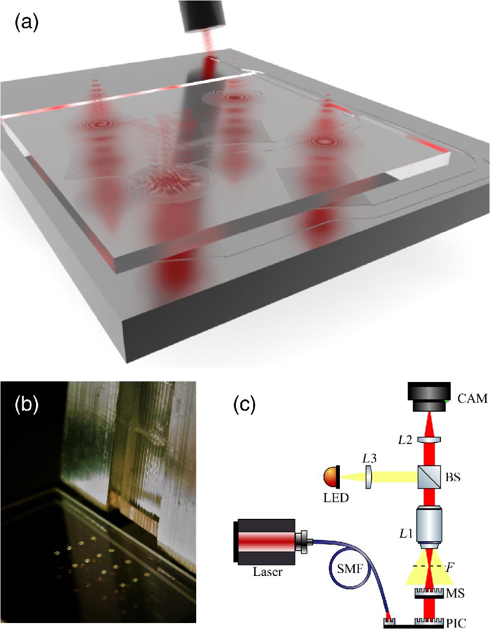
    Fig. 1. Hybrid PIC/metaoptical system. (a) Schematic of the system: an optical fiber feeds the laser light simultaneously to all the apodized gratings in a PIC via waveguides. The light comes out of the gratings, and a separate chip containing an array of metaoptics shapes the grating-output in parallel. (b) Close-up image of the entire hybrid platform with the array of 14 metaoptics, placed on top of the PIC (covered by the metaoptics chip). The optical fiber array shown on the right is used to feed laser light to the PIC. (c) Schematic diagram of the optical setup. SMF, single-mode fiber; MS, metasurface chip; F, focal plane; L1, objective lens (Mitutoyo 10× plan Apo ); BS, beam-splitter cube (Thorlabs CCM1 BS014); L2, plano–convex lens; L3, plano–convex lens; CAM, camera (Point Grey CMLN 13S2M CS). A warm LED is used for alignment and turned off for measurements. In our experiment, the vertical distance between the planes of MS and PIC is kept constant at 1 mm. The microscope is moved vertically to collect light from different planes.
    (a) Optical microscope image of the PIC: 16 identical apodized gratings are fed lights using a single-grating coupler via an optical fiber. (b) Close-up view of the detail of one apodized grating and system of coordinates. (c) Scanning electron microscope (SEM) image of one fabricated apodized grating.
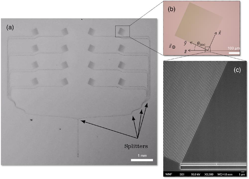
    Fig. 2. (a) Optical microscope image of the PIC: 16 identical apodized gratings are fed lights using a single-grating coupler via an optical fiber. (b) Close-up view of the detail of one apodized grating and system of coordinates. (c) Scanning electron microscope (SEM) image of one fabricated apodized grating.
    Direct measured intensities of light coming from the multifunctional platform. (a) Intensities collected in the plane of the integrated photonic chip showing the 14 apodized gratings “lit” at the same time. The red cross boxes represent defective apodized gratings. (b) Intensities collected in a plane located 1 mm above the metaoptics chip, which is situated at a distance of ∼1 mm above the PIC chip. The red cross boxes represent missing metaoptics. The optical functions of the devices from left to right and from top to bottom are: cubic metalens with focal length at 300 μm and 1 mm, hyperboloid (f=300 μm), hyperboloid (f=1 mm) metalens with 4 levels, 12 levels, and 32 levels, log-asphere (f=1 mm), vortices (l=1, 3, and 15), holograms of seal, W letter and faceprint, and flat-top beam. Notice that at 1-mm collection plane above the chip, the cubic device focal length designed at f=300 μm is still visible, whereas the first hyperboloid (designed with a focal length of 300 μm) is not, highlighting the extended depth of focus of the cubic metaoptics. Some devices also appear dark because their design focal plane was designed at 300 μm while the collection plane is located at 1 mm. Two different scale bars are used to make the figure to show the measured intensities and the separation between each grating/metaoptics. The common large scale bar of 1500 μm refers to the distance between devices, whereas the small scale bar of 300 μm refers to the size of the devices.
    Fig. 3. Direct measured intensities of light coming from the multifunctional platform. (a) Intensities collected in the plane of the integrated photonic chip showing the 14 apodized gratings “lit” at the same time. The red cross boxes represent defective apodized gratings. (b) Intensities collected in a plane located 1 mm above the metaoptics chip, which is situated at a distance of 1  mm above the PIC chip. The red cross boxes represent missing metaoptics. The optical functions of the devices from left to right and from top to bottom are: cubic metalens with focal length at 300  μm and 1 mm, hyperboloid (f=300  μm), hyperboloid (f=1  mm) metalens with 4 levels, 12 levels, and 32 levels, log-asphere (f=1  mm), vortices (l=1, 3, and 15), holograms of seal, W letter and faceprint, and flat-top beam. Notice that at 1-mm collection plane above the chip, the cubic device focal length designed at f=300  μm is still visible, whereas the first hyperboloid (designed with a focal length of 300  μm) is not, highlighting the extended depth of focus of the cubic metaoptics. Some devices also appear dark because their design focal plane was designed at 300  μm while the collection plane is located at 1 mm. Two different scale bars are used to make the figure to show the measured intensities and the separation between each grating/metaoptics. The common large scale bar of 1500  μm refers to the distance between devices, whereas the small scale bar of 300  μm refers to the size of the devices.
    Optical microscope images (upper panel) and measured intensity in the focal plane of corresponding metaoptics (lower panel). (a) Hyperboloid converging lens, (b) vortex 3, and (c) vortex 15. The common scale bar (in blue) measures 50 μm. The orange curves show the horizontal section cut of the 2D intensity.
    Fig. 4. Optical microscope images (upper panel) and measured intensity in the focal plane of corresponding metaoptics (lower panel). (a) Hyperboloid converging lens, (b) vortex 3, and (c) vortex 15. The common scale bar (in blue) measures 50  μm. The orange curves show the horizontal section cut of the 2D intensity.
    Characterization of metaoptical lenses with different depths of field. (a) Hyperboloid metalens, (b) logarithmic asphere metalens, and (c) cubic-phase profile metaoptics. The left panel shows the corresponding optical microscope images. The middle panel shows the cross sections of the propagated beam intensity along the optical axis z. Each cross section is a concatenation of 11 planes along the optical axis, spaced at 25.4 μm, with linear interpolation. The 0 coordinate refers to the design focal plane location (at 1 mm above the PIC), and the corresponding intensities at this plane are shown in the right panel. The orange bar depicts the depth of focus for each device.
    Fig. 5. Characterization of metaoptical lenses with different depths of field. (a) Hyperboloid metalens, (b) logarithmic asphere metalens, and (c) cubic-phase profile metaoptics. The left panel shows the corresponding optical microscope images. The middle panel shows the cross sections of the propagated beam intensity along the optical axis z. Each cross section is a concatenation of 11 planes along the optical axis, spaced at 25.4  μm, with linear interpolation. The 0 coordinate refers to the design focal plane location (at 1 mm above the PIC), and the corresponding intensities at this plane are shown in the right panel. The orange bar depicts the depth of focus for each device.
    Characterization of the holograms. (a) Letter W, (b) faceprint, (c) seal of the University of Washington. Optical microscope images, target hologram, and measured hologram in the designed projection plane are shown in upper, middle, and lower panels, respectively. The common scale bar (in blue) measures 50 μm.
    Fig. 6. Characterization of the holograms. (a) Letter W, (b) faceprint, (c) seal of the University of Washington. Optical microscope images, target hologram, and measured hologram in the designed projection plane are shown in upper, middle, and lower panels, respectively. The common scale bar (in blue) measures 50  μm.
    Quentin A. A. Tanguy, Arnab Manna, Saswata Mukherjee, David Sharp, Elyas Bayati, Yueyang Chen, Karl F. Böhringer, Arka Majumdar. Multifunctional interface between integrated photonics and free space[J]. Advanced Photonics Nexus, 2023, 2(3): 036012
    Download Citation