Quentin A. A. Tanguy1,†, Arnab Manna2, Saswata Mukherjee1, David Sharp2..., Elyas Bayati1, Yueyang Chen1, Karl F. Böhringer1,3 and Arka Majumdar1,2,*|Show fewer author(s)
Abstract
The combination of photonic integrated circuits and free-space metaoptics has the ability to untie technological knots that require advanced light manipulation due to their conjoined ability to achieve strong light–matter interaction via wave-guiding light over a long distance and shape them via large space-bandwidth product. Rapid prototyping of such a compound system requires component interchangeability. This represents a functional challenge in terms of fabrication and alignment of high-performance optical systems. Here, we report a flexible and interchangeable interface between a photonic integrated circuit and the free space using an array of low-loss metaoptics and demonstrate multifunctional beam shaping at a wavelength of 780 nm. We show that robust and high-fidelity operation of the designed optical functions can be achieved without prior precise characterization of the free-space input nor stringent alignment between the photonic integrated chip and the metaoptics chip. A diffraction limited spot of ∼3 μm for a hyperboloid metalens of numerical aperture 0.15 is achieved despite an input Gaussian elliptical deformation of up to 35% and misalignments of the components of up to 20 μm. A holographic image with a peak signal-to-noise ratio of >10 dB is also reported.1 Introduction
With the rise of computational electromagnetics techniques and sophisticated nanofabrication technologies, we can now design and fabricate dielectric photonic structures, with unprecedented reduction in size, and weight while simultaneously increasing their functionalities. These photonic structures are largely of two types: on-chip photonic integrated circuits (PICs), where the light is guided on the chip using waveguides and resonators, and subwavelength-patterned diffractive optics, also known as metaoptics, which shape the optical wavefront in free space.1 The PIC and free-space optics serve two very different purposes: while free-space optics boast a very large space-bandwidth product,2 as well as flexibility and compatibility with existing macroscopic optics,3,4 PICs can enable strong light–matter interaction due to tight spatial confinement of light and longer propagation distance via waveguiding. However, to create a functional compact optical system, we often need both free-space macroscopic optics and PICs. For example, we can envision a spatial light modulator that exploits the PIC to provide the necessary phase shifts, and then an array of metaoptics aggregates the beams and guides in free space. Possible applications include light detection and ranging, and simultaneously controlling a large number of cold atom/ionic qubits. In these applications, often we need stringent control over the optical wavefront, and metaoptics can help clean up the optical beam coming out of the PIC.
To interface PICs with free-space optics, we generally rely on grating couplers,5 which have limited functionality for spatial mode shaping. Thanks to the ability of metaoptics to arbitrarily shape the optical wavefront,6 we can manipulate the output light from the grating couplers to realize a multifunctional interface between PICs and free-space optics. Light coming out of a PIC will be shaped for desired functionalities using different metaoptics, and the wavefront-shaped light will be further routed via additional free-space optics. Such hybrid metaoptics PIC systems will be packaged together and can enable drastically miniaturized optical systems, with potential applications in beam steering,7–10 generation of structured light,11 optical trapping, and manipulation of cold atom qubits.12–14 To that end, researchers have already demonstrated focusing of light coupled from a PIC using metaoptics.7,10,15–18 Additionally, reseachers have demonstrated holography by fabricating metaoptics on top of a PIC.15,17,19 However, no multifunctional coupling between PIC and free space has yet been reported. Here, we report a chip-scale hybrid nanophotonic platform consisting of a 2D array of identical apodized gratings on a PIC and an array of different metaoptics for simultaneously shaping light coming out of each grating in a predefined fashion [Figs. 1(a) and 1(b)]. The PIC and the metaoptics chips are fabricated separately and susbequently aligned, presenting a modular architecture of our hybrid system. We tested the PIC/metaoptics platform at a wavelength of and demonstrated different optical functions, including conventional lensing, extended depth of focusing, vortex beam generation, and holographic projections. In total, we demonstrated simultaneous feeding of light from 14 apodized gratings in a PIC to 14 different metaoptics. Our work shows the ability of such a hybrid PIC/metaoptical platform to create multifunctional optical beams in parallel. Importantly, we show that such a platform does not require stringent alignment (within up to shift measured from the center of the apodized grating). We emphasize that the demonstrated functionalities in this work are chosen as just some examples to highlight the capabilities of this platform. Depending on specific applications, different metaoptics can be designed.

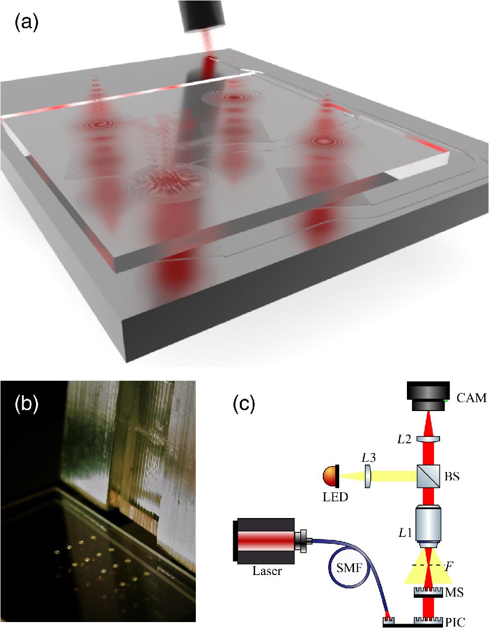
Figure 1.Hybrid PIC/metaoptical system. (a) Schematic of the system: an optical fiber feeds the laser light simultaneously to all the apodized gratings in a PIC via waveguides. The light comes out of the gratings, and a separate chip containing an array of metaoptics shapes the grating-output in parallel. (b) Close-up image of the entire hybrid platform with the array of 14 metaoptics, placed on top of the PIC (covered by the metaoptics chip). The optical fiber array shown on the right is used to feed laser light to the PIC. (c) Schematic diagram of the optical setup. SMF, single-mode fiber; MS, metasurface chip; , focal plane; , objective lens (Mitutoyo plan Apo ); BS, beam-splitter cube (Thorlabs CCM1 BS014); , plano–convex lens; , plano–convex lens; CAM, camera (Point Grey CMLN 13S2M CS). A warm LED is used for alignment and turned off for measurements. In our experiment, the vertical distance between the planes of MS and PIC is kept constant at 1 mm. The microscope is moved vertically to collect light from different planes.
2 Results
A schematic of the hybrid photonic platform is shown in Fig. 1(a), showing different metaoptics (fabricated in a thin film of silicon nitride on the top of a quartz slab) aligned to an array of apodized gratings fabricated in the bottom silicon nitride PIC. We first design -aperture apodized gratings following the approach by Kim et al.20 to output a near-Gaussian beam to free space. These Gaussian beams are then shaped via metaoptics. Figures 1(b) and 1(c) show the fabricated device in the optical characterization setup and a detailed schematic of the optical setup, respectively. It consists of an array of 16 compound devices ( array) with identical apodized gratings [an optical microscope image shown in Fig. 2(a)] and different metaoptics sitting atop of the gratings. Because of fabrication imperfections, two apodized gratings were damaged and could not be probed. Out of the 14 functioning devices [Fig. 1(b)], 8 were retained for extensive characterization. We note that the metaoptical chip blocks the view of the PIC chip underneath in Fig. 1(b).
Sign up for Advanced Photonics Nexus TOC. Get the latest issue of Advanced Photonics Nexus delivered right to you!Sign up now
Figure 2.(a) Optical microscope image of the PIC: 16 identical apodized gratings are fed lights using a single-grating coupler via an optical fiber. (b) Close-up view of the detail of one apodized grating and system of coordinates. (c) Scanning electron microscope (SEM) image of one fabricated apodized grating.
The photonic waveguides and gratings are made in to minimize the losses at the design wavelength of 780 nm. The 16 apodized gratings are connected through a single-entry port grating coupler, requiring a single optical fiber for the integrated photonic chip to function, splitting the input power nearly equally among all of them. While in our experiment, we used a fiber array to input light in the PIC, we used only one fiber in the array, and as such even a single fiber can be used for the experiments reported here. We employed commonly used -junctions (a total of 15 in this case) to split the light into multiple waveguides. As such for gratings, we need splitters. The wavefront generated in free space was purposefully not quantitatively characterized prior to the design of the metaoptics to demonstrate the robustness of the hybrid platform in terms of the ability to reshape the wavefront despite the discrepancies between the design and the real experimental conditions. Optical and scanning electron microscope images of an apodized grating are shown in Figs. 2(b) and 2(c), respectively. The angle of the apodized grating relative to the waveguide was chosen around 24 deg to minimize the divergence of the collimated Gaussian beam. A posteriori characterization of the Gaussian intensity on the grating plane was carried out and is shown in Fig. S1 in the Supplementary Material. A 2D Gaussian fit on the measured intensity of the grating provides a waist of along and along , which is, respectively, 35% and 9% smaller than the target widths. The center of the Gaussian beam is shifted off the center of the grating by on the axis and on the axis on average.
To carry out the design of the PIC and the metaoptics separately, we assumed that an accurate prior knowledge of the free-space field was not necessary to design the phase profiles. In particular, we made three assumptions based on previous studies20 that allowed us to treat the incident field on the metaoptics as a centered plane wave with Gaussian intensity. First, the wavefront error of the Gaussian beam propagating to free space is sufficiently small to be considered a plane wave. Second, the outcoupling angles, defined from the axis, orthogonal to the plane of the grating [see Fig. 2(b)] are also negligible.16 Third, the free-space beam intensity is considered to have a regular (nonelliptical) Gaussian distribution. The details of the design and fabrication of the metaoptics are provided in the Materials and Methods section. We tested 14 different metaoptics and presented detailed results for 8 of them: 5 metalenses [1 with hyperboloid phase profile, 2 vortex beam generators with orbital angular momenta of 3 and 15, and two extended depth-of-focus lenses with logarithmic-asphere and cubic phase profiles] and 3 holograms. The aperture of the metaoptics is kept at to match that of the apodized gratings, although the same aperture size is not crucial for the demonstrated platform. The vertical distance between the PIC and metaoptics chip is , although the performance of our system does not strongly depend on this separation, as the light from the apodized gratings remains collimated over a few millimeters. Figure 3(a) shows the experimentally collected intensities from the array of apodized gratings, and Fig. 3(b) shows the corresponding intensity collected above the metaoptical chip at a plane of 1 mm above, which is the distance of the target projection/focal plane design for 12 out of 14 devices. We found all the apodized gratings to have qualitatively similar behavior. We also note that, as we are interested in a single wavelength operation, the bandwidth of the grating is not important for our measurements (a simulated spectral response is reported in Fig. S2 in the Supplementary Material). Thus, all our beams are shaped simultaneously, which is the key result of our reported multifunctional interface.
Figure 3.Direct measured intensities of light coming from the multifunctional platform. (a) Intensities collected in the plane of the integrated photonic chip showing the 14 apodized gratings “lit” at the same time. The red cross boxes represent defective apodized gratings. (b) Intensities collected in a plane located 1 mm above the metaoptics chip, which is situated at a distance of above the PIC chip. The red cross boxes represent missing metaoptics. The optical functions of the devices from left to right and from top to bottom are: cubic metalens with focal length at and 1 mm, hyperboloid (), hyperboloid () metalens with 4 levels, 12 levels, and 32 levels, log-asphere (), vortices (, 3, and 15), holograms of seal, letter and faceprint, and flat-top beam. Notice that at 1-mm collection plane above the chip, the cubic device focal length designed at is still visible, whereas the first hyperboloid (designed with a focal length of ) is not, highlighting the extended depth of focus of the cubic metaoptics. Some devices also appear dark because their design focal plane was designed at while the collection plane is located at 1 mm. Two different scale bars are used to make the figure to show the measured intensities and the separation between each grating/metaoptics. The common large scale bar of refers to the distance between devices, whereas the small scale bar of refers to the size of the devices.
We characterize the hybrid photonic platform using a fiber-coupled microscopy setup (details are in the Methods section and Fig. S5 in the Supplementary Material). First, we present the results on the vortex beam generators with orbital angular momenta. The upper panel of Figs. 4(a)–4(c) shows the optical microscope images of the vortex phase profiles with of 0, 3, and 15, respectively. The corresponding measured intensities for the same three devices are collected in the design target focal plane (1 mm above the metaoptics) and plotted in the lower panel of Fig. 4. The hyperboloid metalens , designed for a numerical aperture of 0.15, exhibits a diffraction-limited focal spot with a full width at half-maximum (FWHM) of while we observe a 20 dB attenuation of the light intensity at the center of the vortices. The transmission efficiency of the metaoptics was measured at . Details of the efficiency measurement are provided in Fig. S2 in the Supplementary Material. From our rigorous-coupled wave analysis, we expect a transmission efficiency of in these metaoptics. We attribute the discrepancy between the theory and experiment to fabrication imperfection and excess reflection from the substrate. Using antireflecting coating on the other side of the substrate can increase the experimental efficiency.
Figure 4.Optical microscope images (upper panel) and measured intensity in the focal plane of corresponding metaoptics (lower panel). (a) Hyperboloid converging lens, (b) vortex 3, and (c) vortex 15. The common scale bar (in blue) measures . The orange curves show the horizontal section cut of the 2D intensity.
We then compare the hyperboloid, the logarithmic-asphere, and the cubic phase metaoptics21 in terms of their depth of focus. Figures 5(a)–5(c) show these three different metaoptics and their corresponding cross sections in the left panel. As expected, both the logarithmic-asphere and cubic-phase mask exhibit a longer depth of focus compared to the hyperboloid metalens.22,23 The hyperboloid lens has a depth of focus of , whereas the logarithmic-asphere metalens exhibits a two-fold increase in depth of focus. The logarithmic-asphere device also has a larger focal spot () than the hyperboloid (). The depth of focus of the cubic metaoptics exceeds the boundaries of the measured depth range. The latter demonstrates a Gaussian central spot of FWHM, and the direct neighboring peak intensity drops by 37% compared with the central one. The rays parallel to the chief ray are due to the cubic-phase inherent distortion. Essentially, the cubic phase generates an accelerating Airy beam.24,25
Figure 5.Characterization of metaoptical lenses with different depths of field. (a) Hyperboloid metalens, (b) logarithmic asphere metalens, and (c) cubic-phase profile metaoptics. The left panel shows the corresponding optical microscope images. The middle panel shows the cross sections of the propagated beam intensity along the optical axis . Each cross section is a concatenation of 11 planes along the optical axis, spaced at , with linear interpolation. The 0 coordinate refers to the design focal plane location (at 1 mm above the PIC), and the corresponding intensities at this plane are shown in the right panel. The orange bar depicts the depth of focus for each device.
Finally, we characterize a set of three different holograms fabricated on the same chip. The upper panel of Figs. 6(a)–6(c) shows optical images of their phase masks. Binary intensities of the target holograms are shown in the middle panel, and the intensity of the fabricated holograms are plotted in the lower panel. We observe a good fidelity between the holograms and their corresponding ground truth. According to the peak signal-to-noise ratio (PSNR), the “faceprint” hologram [Fig. 6(b)] shows the highest fidelity with a value of 11.4 while the “seal” and the “” hologram rank second and third with PSNR values of 5 and 4.7, respectively. A possible explanation for the higher score of the faceprint hologram may be related to its smaller size. As in our Gerchberg–Saxton algorithm,26 the angular spectrum propagation method27 is based on fast Fourier transforms of the fields, the size of the field impacts the higher spatial cut-off frequencies, causing the retrieved phase of the larger holograms to lose more bandwidth.
Figure 6.Characterization of the holograms. (a) Letter , (b) faceprint, (c) seal of the University of Washington. Optical microscope images, target hologram, and measured hologram in the designed projection plane are shown in upper, middle, and lower panels, respectively. The common scale bar (in blue) measures .
3 Discussion
We exploited metaoptics’ ability to shape optical wavefronts to create a multifunctional interface between integrated photonics and free-space optics. Although all the light beams coming out of the PIC are identical, by placing a different metaoptics on top of each grating, we can simultaneously manipulate all the beams differently. Specifically, the demonstration of holography provides an opportunity to engineer the beam shape to any desired functionality. If the light beam coming out of the PIC has some nonidealities due to fabrication imperfections, an additional metaoptics can be designed and fine-tuned to reshape the beam. Furthermore, metaoptics can provide an additional momentum vector to different beams, allowing light beams coming from gratings at different locations on the chip to form an ordered array of beams in free space. Such ability to reshape multiple beams can be particularly useful for active photonics. By placing the active components far from each other in a PIC, we can reduce the energy density and routing complexity of control circuits. However, using a separate layer of passive metaoptics, we can aggregate these beams in an ordered array. Such aggregation of beams for holography could be an interesting future direction. Interestingly, we found the alignment accuracy of the metaoptics and PICs can be in the orders of , making the co-packaging of these devices significantly simpler. We envision our demonstrated hybrid PIC/metaoptics platform will allow combining the best of both technologies: large space-bandwidth product and active functionalities exploiting strong light–matter interaction, with far-reaching impact on the field of optical information science (both classical and quantum) and imaging.
4 Methods
4.1 Design
The design and fabrication of the PIC follows previous reports.20 A standard straight-trench grating coupler was designed to couple an optical fiber to the PIC.5 The grating coupler is connected to a network of waveguides splitters (15 of them) into 16 lines to irrigate the distal photonic devices, as shown in Fig. 2(a). Each waveguide is terminated by a tapered profile to leak the waveguide mode into a 1D collimated Gaussian slab mode. The waveguide-to-slab mode conversion step was accomplished using a fully etched waveguide, and the coupling distance between the waveguide and the slab was tapered from 1 to over a length of to generate the tilted Gaussian slab mode incident on the apodized grating. Then, each apodized grating outcouples the slab mode into a free-space 2D Gaussian mode. The apodized gratings were partially etched over 60 nm deep and designed to generate a waist of . The grating period and grating width were tapered from 410 to and 20 to 100 nm, respectively, over a length of . The components of the photonic chip were designed for a wavelength of 780 nm using a 220-nm-thick platform encapsulated with -like refractive index materials. More features on the spectral response of the apodized gratings are provided in Fig. S2 in the Supplementary Material.
Both analytical and numerical methods were used for the design of the metaoptics. First, a library of meta-atoms was generated to maximize the transmitted intensity and achieve a phase coverage at the designed wavelength.28 The details of the meta-atoms and the phase-to-pillar size trend are provided in Fig. S3 in the Supplementary Material. The metaoptics exhibiting focusing behavior were designed using analytical spatial phase profiles. The metalens and the two vortex phase distributions are given by
While gives the phase profile for the hyperboloid lens, the vortex beams are designed with orbital angular momentum of and 15, respectively. and represent the cylindrical coordinates of the phase mask and , the focal length, is set at 1 mm. The spatial phase profile of the logarithmic-asphere metaoptics is given by21where is the aperture radius; and and denote two ends of the depth of focus. We chose and for our case. The cubic phase profile is given by where the parameter denotes the strength of the cubic term and is chosen as and . In all these lenses is kept at .
The phase profiles of the three holograms were retrieved using a modified Gerchberg–Saxton algorithm along with an angular spectrum method to project the hologram at a given plane above the metaoptics slab. For the sake of simplifying the characterization, the projection planes of the all the metaoptics were designed at a distance on the axis. The phase masks were then converted to a grid of meta-atoms arranged on a square lattice (as shown in Fig. S3 in the Supplementary Material).
4.2 Fabrication Process
The PIC was fabricated in two steps. First, a 220 nm on a buffer oxide chip was spin-coated with a 400-nm-thick layer of ZEP-520A electron-beam lithography (EBL) resist, and a 100 kV EBL system (JEOL JBX6300FS) was used to define the waveguide grating coupler, 330-nm-wide waveguides, and slab mode coupling waveguides. The fully etched pattern was transferred using a dry reactive ion etch (RIE) consisting of chemistry. A second EBL step with a 150-nm-thick layer of the same resist was then used to define the apodized gratings, which were then partially etched to a target depth of 60 nm. The entire chip was later spin-coated with a thick layer of polymethyl methacrylate (PMMA) to conveniently mimic the refractive index of .
Metaoptics were fabricated on a -thick -fused silica chip using a standard nanofabrication process. A layer of 780 nm of was deposited by plasma-enhanced chemical vapor deposition (PECVD) at 350°C. A 300-nm-thick layer of ZEP 520A followed by a thin film of anticharging polymer (DisCharge ) were spin-coated on the . The resist was then exposed using the same EBL tool at 8 nA to form the nanoscatterer patterns. The resist was developed for 2 min in amyl acetate after removal of the conductive polymer in water. A 70-nm-thick hard mask was evaporated and lifted off in a bath of 1-methyl-2-pyrrolidone at 90°C overnight followed by a short ultrasonication in dichloromethane. Due to the short distance between the apodized gratings and the optical fiber coupling on the PIC, and because the metaoptics must be aligned to the gratings, the fused silica chip was diced to make the patterns closer to the edge to leave sufficient space to approach the optical fiber. To form the nanopillars, the patterns were transferred using a fluorine-based RIE process, leaving a total thickness of 10 nm of on top of 778 nm of . For the RIE step, the chips were bonded to a Si carrier wafer using a vacuum oil for thermal contact spread underneath the entire surface of the chip. Finally, the chip was unbonded in acetone and descummed in a gentle plasma. Additional SEM pictures of the holograms are given in Fig. S4 in the Supplementary Material.
4.3 Characterization
To characterize the compound platform, a custom microscope composed of a long working distance objective lens aligned to a plano–convex lens with a visible camera was mounted onto an XYZ stage above the platform. A warm light-emitting diode (LED) light delivered from an optical fiber, collimated, and split through a beam-splitter cube inserted between the objective and the plano–convex lens was used for alignment and imaging purposes. The metaoptics slab was mounted onto a five-degree-of-freedom stage (XYZ + pitch + roll) for precise alignment to the photonic chip. The photonic chip was fixed to a four-degree-of-freedom stage (XYZ + yaw) for fine adjustment purposes. Details of the optical setup are provided in Fig. 1(c) and Fig. S5 in the Supplementary Material. A single fiber—from the fiber array shown in Fig. 1(b)—was used and coupled to the grating coupler. The metaoptics array was then aligned to the PIC. Finally, the microscope was used to image the optical functions produced by each device.
Quentin A. A. Tanguy received his MEng degree from French National Graduate School of Mechanical Engineering and Microtechnologies (ENSMM) of Besançon, France in 2013 and his PhD from the University of Franche-Comté (Femto-ST Research Institute, France) in 2018 in exchange with the University of Florida. He is currently working as a postdoctoral fellow at the University of Washington on MEMS and metasurfaces. His research interest includes hybrid photonic platforms, imaging, and holography.
Arnab Manna received his BTech and MTech degrees in Electrical Engineering with a specialization in microelectronics from the Indian Institute of Technology Bombay, India. Currently, he is pursuing a PhD in the Department of Physics, the University of Washington. His research interests include integrated photonics, quantum materials, and nanomechanics.
Saswata Mukherjee received his PhD in imaging through scattering media from BGU Beersheva, where he developed new imaging techniques through scattering materials. He is a researcher in the field of optics, with a keen interest in the areas of meta-optics, Fourier optics, and diffractive optics. During his postdoctoral fellowship at the University of Washington, he explored the potential of meta-optics for holographic applications.
David Sharp is currently pursuing a PhD in physics at the University of Washington. His research primarily focuses on coupling solution-processed semiconductor nanocrystals to dielectric nanocrystals. The goal of his research is to enable scalable photonic devices based on low-power optical nonlinearities.
Elyas Bayati received his PhD in electrical engineering from the University of Washington. His research focused on design, fabrication, and characterization of metasurfaces to build systems for imaging and non-imaging applications. He has designed composite metasurfaces for an ultracompact near-eye visors concept for an immersive augmented reality experience. In addition, he has interned in Microsoft Research, Apple, and Samsung Semiconductor on diffractive optics related topics and currently works in Tunoptix as a senior optical engineer.
Yueyang Chen received his PhD in electrical engineering from the University of Washington. His PhD research primarily focuses on coupling solution-processed material and 2D materials to nanophotonic devices. The goal of his research is to enable scalable photonic devices for both classical and quantum applications.
Karl F. Böhringer received his Dipl.-Inform. degree from the University of Karlsruhe, Germany and his MS/PhD degrees in computer science from Cornell University. He is a professor in the Department of Electrical and Computer Engineering and Bioengineering at the University of Washington, where his research focuses on micro/nano electro mechanical systems, self-assembly, microfluidics, and micro-optics. He is the director of the Institute for Nano-engineered Systems and site director of the NSF National Nanotechnology Coordinated Infrastructure site at the University of Washington.
Arka Majumdar received BTech degree from IIT-Kharagpur in 2007, his MS degree in 2009, and his PhD in 2012 in electrical engineering from Stanford University. He is an associate professor in the Departments of Electrical and Computer Engineering and Physics at the University of Washington. His research interests include developing a hybrid nanophotonic platform using emerging material systems for optical information science, imaging, and microscopy.
References
[1] S. Zhang et al. High efficiency near diffraction-limited mid-infrared flat lenses based on metasurface reflectarrays. Opt. Express, 24, 18024(2016).
[2] A. W. Lohmann et al. Space–bandwidth product of optical signals and systems. J. Opt. Soc. Am., 13, 470(1996).
[3] N. Yu et al. Light propagation with phase discontinuities: generalized laws of reflection and refraction. Science, 334, 333-337(2011).
[4] W. T. Chen et al. Broadband achromatic metasurface-refractive optics. Nano Lett., 18, 7801-7808(2018).
[5] R. Marchetti et al. Coupling strategies for silicon photonics integrated chips. Photonics Res., 7, 201(2019).
[6] S. M. Kamali et al. A review of dielectric optical metasurfaces for wavefront control. Nanophotonics, 7, 1041-1068(2018).
[7] Y.-C. Chang et al. 2D beam steerer based on metalens on silicon photonics. Opt. Express, 29, 854(2021).
[8] F. S. Chau, G. Zhou, Y. Zou. Ultra-compact optical zoom endoscope using solid tunable lenses. Opt. Express, 25, 20675-20688(2017).
[9] G. Zhou et al. Metasurface-based Fourier lens fed by compact plasmonic optical antennas for wide-angle beam steering. Opt. Express, 30, 21918(2022).
[10] W.-B. Lee et al. Metasurface doublet-integrated bidirectional grating antenna enabling enhanced wavelength-tuned beam steering. Photonics Res., 10, 248(2021).
[11] Q. Wang et al. On‐chip generation of structured light based on metasurface optoelectronic integration. Laser Photonics Rev., 15, 2000385(2021).
[12] M. T. Hummon et al. Photonic chip for laser stabilization to an atomic vapor with 10–11 instability. Optica, 5, 443(2018).
[13] A. Liu et al. Multigrating design for integrated single-atom trapping, manipulation, and readout. Phys. Rev. A, 105, 053520(2022).
[14] A. Y. W. Zhu et al. High NA free-space focusing using a metasurface-integrated photonic platform for atom trapping(2019).
[15] Y. Ding et al. Metasurface-dressed two-dimensional on-chip waveguide for free-space light field manipulation. ACS Photonics, 9, 398-404(2021).
[16] A. Yulaev et al. Metasurface-integrated photonic platform for versatile free-space beam projection with polarization control. ACS Photonics, 6, 2902-2909(2019).
[17] P.-Y. Hsieh et al. Integrated metasurfaces on silicon photonics for emission shaping and holographic projection. Nanophotonics, 4687-4695(2022).
[18] X. Guo et al. Molding free-space light with guided wave–driven metasurfaces. Sci. Adv., 6, eabb4142(2020).
[19] Y. Shi et al. On-chip meta-optics for semi-transparent screen display in sync with AR projection. Optica, 9, 670(2022).
[20] S. Kim et al. Photonic waveguide to free-space Gaussian beam extreme mode converter. Light Sci. Appl., 7, 72(2018).
[21] L. Huang et al. Design and analysis of extended depth of focus metalenses for achromatic computational imaging. Photonics Res., 8, 1613(2020).
[22] N. George, W. Chi. Extended depth of field using a logarithmic asphere. J. Opt. Pure Appl. Opt., 5, S157-S163(2003).
[23] A. Zhan et al. Metasurface freeform nanophotonics. Sci. Rep., 7, 1673(2017).
[24] M. A. Bandres. Accelerating beams. Opt. Lett., 34, 3791(2009).
[25] Z. Fang et al. 1D self-healing beams in integrated silicon photonics. ACS Photonics, 8, 2139-2147(2021).
[26] R. W. Gerchberg. A practical algorithm for the determination of phase from image and diffraction plane pictures. Optik, 35, 237-246(1972).
[27] J. W. Goodman. Introduction to Fourier Optics(2005).
[28] A. Zhan et al. Low-contrast dielectric metasurface optics. ACS Photonics, 3, 209-214(2016).