
Nian Liu, Xue Zhao, Mengling Xia, Guangda Niu, Qingxun Guo, Liang Gao, Jiang Tang. Light-emitting diodes based on all-inorganic copper halide perovskite with self-trapped excitons[J]. Journal of Semiconductors, 2020, 41(5): 052204
- Journal of Semiconductors
- Vol. 41, Issue 5, 052204 (2020)
Abstract
1. Introduction
Organometal halide perovskites have attracted great attention as emitting materials of high efficient light-emitting diodes (LEDs) for their unique advantages such as high color purity, tunable bandgap and facial solution processibility[
Despite most of the Pe-LEDs are fabricated via solution processing, vacuum-based deposition (VBD) is more favorable for the fabrication of high performance LEDs. Because of the controllable environment of vacuum preparation, devices fabricated by VBD are highly reproducible and reliable[
Recently, a set of high performance all-inorganic perovskites CsCu2I3 and Cs3Cu2I5 have been reported[
Further research confirmed that the electron–phonon interaction is so strong in these materials that the excited electrons and holes would cause elastic distortions in the lattice surrounding them as self-trapped excitons (STEs)[
Herein, CsCu2I3 powder was successfully synthesized with a high photoluminescence quantum yield (PLQY) of nearly 20%. Bright yellow emission could be observed under UV light excitation, with a emission peak located at 560 nm and a quite broad full width at half maximum (FWHM) of nearly 180 nm due to STE emission[
2. Experiment
2.1. Materials
All chemicals were used without further purifications: CsI (cesium iodide, 99%, Aladdin Reagent Ltd); CuI (cuprous iodide, 99%, Aladdin Reagent Ltd); DMSO (dimethyl sulfoxide, AR99%, Aladdin Reagent Ltd); LiF (lithium fluoride, 99.99%, Aladdin Reagent Ltd); TPBi (Xi’an Polymer Light Technology Corp); Aluminum particles (99.99%, Xi’an Polymer Light Technology Corp).
2.2. Synthesis of CsCu2I3 powder
CsCu2I3 powder was synthesized using a simple and efficient one-step reaction. In the reaction, 1.45 g CsI and 2.11 g CuI were added in 9 mL DMSO and stirred for 2 h at 70 °C for complete dissolution. Then, the solution was heated to 90 °C to evaporate the solvent and the resulting precipitate was CsCu2I3 powder that we needed.
2.3. LED device fabrication
Etched indium tin oxide (ITO) glass substrates were cleaned sequentially with detergent, acetone, isopropyl alcohol and ethanol by sonication for 20 min of each step, then dried with nitrogen. 20 nm Li doped NiOx was deposited on the ITO glasses by magnetron sputtering, with a radio frequency power of 200 W for 2 min. During the NiOx deposition, the substrates were held at 200 °C with a Ar2/O2 flow ratio of 99, and the vacuum was kept lower than 10–3 Pa. Afterwards, the synthesized CsCu2I3 powder was deposited on the room-temperature NiOx by vacuum-based deposition without further annealing. Next, a layer of 20 nm TPBi and patterned LiF (1 nm)/Al (80 nm) electrodes were deposited by thermal evaporation to complete the device fabrication. The deposition rates of CsCu2I3, TPBi, LiF and Al were kept at 0.2, 0.1, 0.02, and 0.2 nm/s, respectively. The rates were precisely monitored by calibrated quartz crystal. The vacuum was kept under 10-4 Pa during the whole deposition process.
2.4. Materials and devices characterization
The XRD data was accumulated using a Philips X'Pert Pro diffractometer with Cu Kα radiation (λ = 1.54 Å). The photoluminescence (PL) and photoluminescence exciation (PLE) spectra of the CsCu2I3 film were measured using an Edinburgh FLS980 spectrofluorometer. The absolute PLQY was further determined with an integrated sphere. The morphology of CsCu2I3 film was characterized by FEI Nova Nano field-emission SEM. Keithley 2400 Sourcemeter and Photo Research Spectra Scan PR655 were programmed and used to record the J−V−L curves, EQE, and CRI color coordinates of the operating Pe-LEDs.
3. Results and discussion
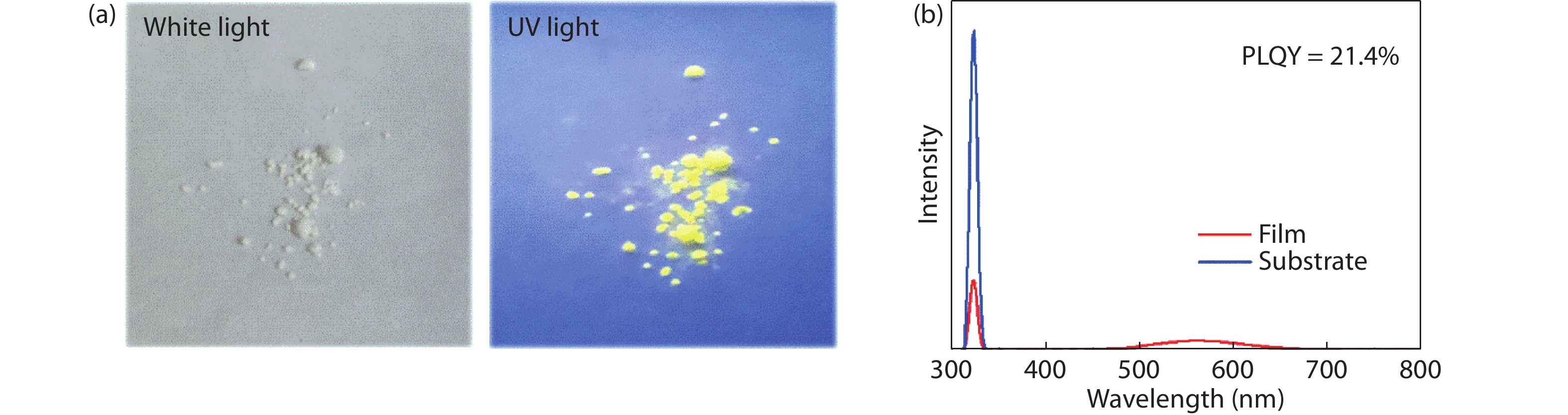
In this work, we used a simple one-step way to successfully synthesize CsCu2I3 powder. Fig. 1(a) shows optical images of the synthesized CsCu2I3 powder under natural light and excited by ultraviolet light. The synthesized white CsCu2I3 powder under natural light emits bright yellow light under ultraviolet excitation. Then the precise PLQY of the CsCu2I3 powder is furthered confirmed as shown in Fig. 1(b). After calibration calculation, the absolute PLQY of the CsCu2I3 powder is 21.4%.
![]()
Figure 1.(Color online) (a) Optical images of synthesized CsCu2I3 powder under natural light and excited by ultraviolet light. (b) PLQY of the CsCu2I3 powder.
The synthesized CsCu2I3 powder shows excellent air and thermal stability, whose decomposition temperature is as high as 600 °C, as confirmed in the early work[
![]()
Figure 2.(Color online) (a) XRD patterns of the CsCu2I3 film and powder. (b) Schematic of CsCu2I3 crystal structure. (c) PLE and PL spectra of the CsCu2I3 film. (d) Schematic of the energy level structure of STE.
As CsCu2I3 is a reported environmentally friendly material with excellent PLQY and thermal stability[
![]()
Figure 3.(Color online) (a) Structure of CsCu2I3 Pe-LED. (b) Schematic of VBD for CsCu2I3 film. (c) SEM image of CsCu2I3 film. (d) Energy level diagram of CsCu2I3 device.
The current density–voltage–luminance (J–V–L) characteristics and external quantum efficiency (EQE) versus luminance are described in Figs. 4(a) and 4(b). The resulting device shows a relatively low turn-on voltage of 2.9 V at the luminance of 1 cd/m2. It exhibits the maximum luminance of 10 cd/m2 and the best EQE is 0.02% at 1 cd/m2. Fig. 4(c) shows an image of the operating Pe-LEDs and the CIE color coordinates. It emits bright yellow light with a greatly broad FWHM just same as the PL results, which is attribute to the STE emission. The measured CIE color coordinate is (0.489, 0.485) as shown in Fig. 4(c). It is believed that the successful realization of the STE electroluminescence based on CsCu2I3 would make a step further in the aspect of wide spectrum electroluminescence. And much more continuous works are expected to further improve device brightness and luminescence.
![]()
Figure 4.(Color online) (a) Current density–voltage (
4. Conclusion
In summary, we synthesized the CsCu2I3 powder with PLQY exceeding 20% by a simple method. By taking advantage of its excellent thermal stability, the uniform and stable CsCu2I3 film was successfully fabricated by the direct evaporation of CsCu2I3 powder through VBD technology. We further characterized the VBD CsCu2I3 film by XRD and the pure phase of was determined. For the CsCu2I3 film prepared by VBD, the morphology was observed with flat surface and dense grains. The CsCu2I3 Pe-LED emitted bright yellow light with a quite broad FWHM attributed to the STE emission. It showed the maximum luminance of 10 cd/m2 and the best EQE is 0.02%. As far as we know, it is the first time of the successful realization of the STE electroluminescence based on CsCu2I3 through the advanced VBD technology. Despite its relatively low brightness and efficiency at present, the great improvement of the device performance could be sincerely expected with the further optimization of the device structure. We believe this work would provide a new avenue for high quality Pe-LED, and promote the further exploration of its working mechanism.
Acknowledgments
This work was supported by the National Key R&D Program of China (2016YFB070700702), the National Natural Science Foundation of China (51761145048), the Fundamental Research Funds for the Central Universities (HUST: 2019421JYCXJJ004) and the China Postdoctoral Science Foundation Grant (2019M662624). The authors thank the Analytical and Testing Center of HUST.
References
[1] L N Quan, B P Rand, R H Friend et al. Perovskites for next-generation optical sources. Chem Rev, 119, 7444(2019).
[2] A Fakharuddin, U Shabbir, W Qiu et al. Inorganic and layered perovskites for optoelectronic devices. Adv Mater, 31, e1807095(2019).
[3] D Luo, Q Chen, Y Qiu et al. Device engineering for all-inorganic perovskite light-emitting diodes. Nanomaterials, 9, 1007(2019).
[4] M Lu, Y Zhang, S Wang et al. Metal halide perovskite light-emitting devices: promising technology for next-generation displays. Adv Funct Mater, 29, 1902008(2019).
[5] Q Wang, X Wang, Z Yang et al. Efficient sky-blue perovskite light-emitting diodes via photoluminescence enhancement. Nat Commun, 10, 5633(2019).
[6] M Ban, Y Zou, J P H Rivett et al. Solution-processed perovskite light emitting diodes with efficiency exceeding 15% through additive-controlled nanostructure tailoring. Nat Commun, 9, 3892(2018).
[7] X Zhao, Z K Tan. Large-area near-infrared perovskite light-emitting diodes. Nat Photon, 14, 215(2019).
[8] Y Cao, N Wang, H Tian et al. Perovskite light-emitting diodes based on spontaneously formed submicrometre-scale structures. Nature, 562, 249(2018).
[9] K Lin, J Xing, L Quan et al. Perovskite light-emitting diodes with external quantum efficiency exceeding 20 percent. Nature, 562, 245(2018).
[10] H Cho, Y H Kim, C Wolf et al. Improving the stability of metal halide perovskite materials and light-emitting diodes. Adv Mater, 30, e1704587(2018).
[11] P Cheng, L Sun, L Feng et al. Colloidal synthesis and optical properties of all-inorganic low-dimensional cesium copper halide nanocrystals. Angew Chem Int Ed Engl, 58, 16087(2019).
[12] T Jun, K Sim, S Iimura et al. Lead-free highly efficient blue-emitting Cs3Cu2I5 with 0D electronic structure. Adv Mater, 30, e1804547(2018).
[13] J Luo, X Wang, S Li et al. Efficient and stable emission of warm-white light from lead-free halide double perovskites. Nature, 563, 541(2018).
[14] P Vashishtha, G V Nutan, h B E Griffith et al. Cesium copper iodide tailored nanoplates and nanorods for blue, yellow, and white emission. Chem Mater, 31, 9003(2019).
[15] B M Benin, D N Dirin, V Morad et al. Highly emissive self-trapped excitons in fully inorganic zero-dimensional tin halides. Angew Chem Int Ed Engl, 57, 11329(2018).
[16] Y Hu, Q Wang, Y L Shi et al. Vacuum-evaporated all-inorganic cesium lead bromine perovskites for high-performance light-emitting diodes. J Mater Chem C, 5, 8144(2017).
[17] R Lin, Q Guo, Q Zhu et al. All-inorganic CsCu2I3 single crystal with high-PLQY (≈15.7%) intrinsic white-light emission via strongly localized 1D excitonic recombination. Adv Mater, 31, 1905079(2019).
[18] W Chen, J Zhang, G Xu et al. A semitransparent inorganic perovskite film for overcoming ultraviolet light instability of organic solar cells and achieving 14.03% efficiency. Adv Mater, 30, e1800855(2018).
[19] X Zhu, D Yang, R Yang et al. Superior stability for perovskite solar cells with 20% efficiency using vacuum co-evaporation. Nanoscale, 9, 12316(2017).
[20] M Liu, M B Johnston, H J Snaith. Efficient planar heterojunction perovskite solar cells by vapour deposition. Nature, 501, 395(2013).
[21] E R Dohner, A Jaffe, L R Bradshaw et al. Intrinsic white-light emission from layered hybrid perovskites. J Am Chem Soc, 136, 13154(2014).
[22] M D Smith, B L Watson, R H Dauskardt et al. Broadband emission with a massive stokes shift from sulfonium Pb–Br hybrids. Chem Mater, 29, 7083(2017).
[23] S Wang, Y Yao, J Kong et al. Highly efficient white-light emission in a polar two-dimensional hybrid perovskite. Chem Commun, 54, 4053(2018).
[24] S Krishnamurthy, R Naphade, J Mir Wasim et al. Molecular and self-trapped excitonic contributions to the broadband luminescence in diamine-based low-dimensional hybrid perovskite systems. Adv Optical Mater, 1800751(2018).
[25] S Li, Q Hu, J Luo et al. Self-trapped exciton to dopant energy transfer in rare earth doped lead-free double perovskite. Adv Opt Mater, 7, 1901098(2019).
[26] S Li, J Luo, J Liu et al. Self-trapped excitons in all-inorganic halide perovskites: fundamentals, status, and potential applications. J Phys Chem Lett, 10, 1999(2019).
[27] M D Smith, H I Karunadasa. White-light emission from layered halide perovskites. Acc Chem Res, 51, 619(2018).
[28] J Li, u P Du, S Li et al. High-throughput combinatorial optimizations of perovskite light-emitting diodes based on all-vacuum deposition. Adv Funct Mater, 29, 1903607(2019).
[29] P Du, J Li, L Wang et al. Vacuum-deposited blue inorganic perovskite light-emitting diodes. ACS Appl Mater Interfaces, 11, 47083(2019).
[30] Z Ma, Z Shi, C Qin et al. Stable yellow light-emitting devices based on ternary copper halides with broadband emissive self-trapped excitons. ACS Nano, 14, 4475(2020).


Set citation alerts for the article
Please enter your email address

© Copyright 2018-2021 | Chinese Laser Press. All Rights Reserved 沪ICP备15018463号-20