
Dongzhou Zhong. Control of the polarization switching and the nonlinear dynamic behaviors of vertical cavity surface-emitting lasers with external optical injection[J]. Chinese Optics Letters, 2015, 13(Suppl.): S21405
- Chinese Optics Letters
- Vol. 13, Issue Suppl., S21405 (2015)
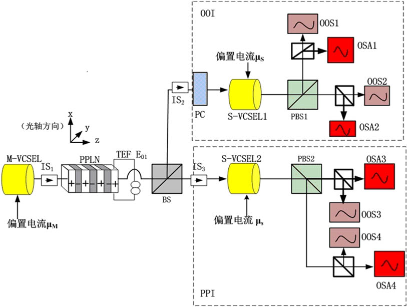
Fig. 1. Schematic of the control scheme for the PS and the NDBs of optically injected VCSEL.
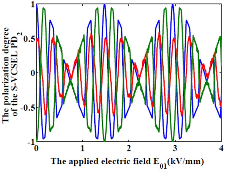
Fig. 2. For different bias current μ M PD 2 E 01 μ S = 1.2 K i n j = 10 ns − 1 E 02 = 0 kV / mm μ M = 1.048 μ M = 1.048 μ M = 1.1
Fig. 3. PS law of the output light from S-VCSEL2 in one change period of the applied electric field E 01 μ M = 1.048
Fig. 4. PS law of the output light from S-VCSEL2 in one change period of the applied electric field E 01 μ M = 1.1
Fig. 5. PS law of the output light from S-VCSEL2 in one change period of the applied electric field E 01 μ M = 1.18
Fig. 6. For different bias current μ M PD 2 E 01 μ S = 1.2 K i n j = 10 ns − 1 E 02 = 0 kV / mm μ M = 1.048 μ M = 1.048 μ M = 1.1
Fig. 7. Under different the applied electric field E 01 x y μ S = 1.2 μ M = 1.18 k i n j = 10 ns − 1 E 02 = 0 kV / mm x -LP; red-line: y -LP. E 0 = 0 0.6849 1.326 1.474 kV / mm
Fig. 8. Under different the applied electric field E 01 x y μ S = 1.2 μ M = 1.18 k i n j = 10 ns − 1 E 02 = 0 kV / mm x -LP; red-line: y -LP. E 0 = 0 0.6849 1.326 1.474 kV / mm

Set citation alerts for the article
Please enter your email address
© Copyright 2018-2021 | Chinese Laser Press. All Rights Reserved 沪ICP备15018463号-20