Dongzhou Zhong. Control of the polarization switching and the nonlinear dynamic behaviors of vertical cavity surface-emitting lasers with external optical injection[J]. Chinese Optics Letters, 2015, 13(Suppl.): S21405
Copy Citation Text
For polarization switching (PS) and nonlinear dynamic behaviors (NDBs) of an optically injected laser system composed of a master vertical-cavity surface-emitting laser (VCSEL) and a slave VCSEL, we put forward a novel manipulation scheme by means of electro-optic (EO) modulation with quasi-phase matched technology. It is found that the PS of the slave VCSEL subject to parallel or orthogonal optical injection takes on a change of periodic oscillation with the applied transverse electric field. The optically injected slave VCSEL can experience different NDBs evolutions when the light from the master laser is modulated by the linear EO effect.
Vertical-cavity surface-emitting lasers (VCSELs) have extensive applications, ranging from optical switching, all-optical composite logic gate, optical interconnection, optical storage, optical communication, to photonic information processing. This is due to their excellent characteristics such as low threshold current, single-longitudinal-mode operation, low power consumption, reduced manufacturing costs, circular output beam, and high bandwidth modulation. According to the spin flip model (SFM)[1], the light emitted by the VCSEL always includes two mutually orthogonal linear-polarization (LP) mode components because that there is weak anisotropy of the gain medium or laser cavity. The output of the laser can be , or circular polarization (CP), or elliptic polarization (EP), owing to that the polarization prefers different orientation[2]. Although VCSELs are intrinsically single-longitudinal mode devices, they usually show complex polarization characteristics and their polarization switching (PS) is sensitive to a slight disturbance of external light[3–13].
It is crucial that the PS and the nonlinear dynamic behavior (NDBs) of VCSELs are controlled steadily in polarization-sensitive applications such as optical switching, all-optical composite logic gate, and so on. Optical injection is also a technique used to control or achieve PS and NDBs. For VCSEL, there are two methods of optical injection[14]. One is parallel optical injection (POI), and the other one is orthogonal optical injection (OOI). In the system composed of master VCSEL (M-VCSEL) and slave VCSEL (S-VCSEL), it is defined as POI when the - and -LP of the M-VCSEL are injected into the - and -LP of the S-VCSEL, respectively. It is named as OOI when the - and -LP from the M-VCSEL are injected into the - and -LP of the S-VCSEL, respectively. In recent years, by controlling two key parameters, such as the injected optical power and the bias current, the PS and the evolutions of NDBs have been observed theoretically and experimentally in single-transverse mode VCSEL with POI or OOI[3–14]. However, the fierce competition between two LP components from the output of VCSEL may be manifested as a slight variation of the two key parameters. As a result, the output polarization becomes extremely unstable and the evolution of the NDBs of each LP component appear an unstable state. It is rather difficult to steadily and accurately control the PS and the evolution of the NDBs by changing the injected optical power and the bias current. Additionally, the optically injected VCSEL does not readily emit a steady CP mode, which is used for specific fields. The prospects of the optically injected VCSELs in applications are limited by these unfavorable factors. For this purpose, according to the new theory of electro-optic (EO) modulation[15], in this Letter we put forward a novel control scheme for the PS and the evolution of NDBs of injected optically VCSEL. In the scheme, the S-VCSEL with POI or OOI can emit an arbitrary polarization mode and generate different NDBs. whereas the output light from the M-VCSEL is modulated by the linear EO effect.
The physical basis of EO modulation is the linear EO effect. In 2001, instead of the refractive index ellipsoid theory, the wave-coupling theory has been used for the EO effect[15]. This theory can apply to the case of any pulses propagating along an arbitrary direction in any crystal, under an applied electric field along an arbitrary direction. According to this theory, the efficiency of the linear EO effect depends on the phase match between two LP components of the optical field. In the case of the phase matching technique, the technology of the quasi-phase-matching based on optical superlattice crystals shows many advantages over that of the birefringence phase matching, as follows. It can be easily performed in engineering, and applies to all transparent wavelengths and the maximum EO coefficient of the EO crystal. Periodically poled lithium niobate (PPLN), as a typical optical superlattice crystal, has good EO performance. Consequently, a PPLN crystal is used in the context of the phase matching of the linear EO effect[16–18]. Based on the aforementioned considerations, we explore the manipulation scheme of the PS and NDBs of an optically injected VCSEL, by means of the wave-coupling theory of quasi-phase-matching for the linear EO effect in a PPLN crystal.
Sign up for Chinese Optics Letters TOC. Get the latest issue of Chinese Optics Letters delivered right to you!Sign up now
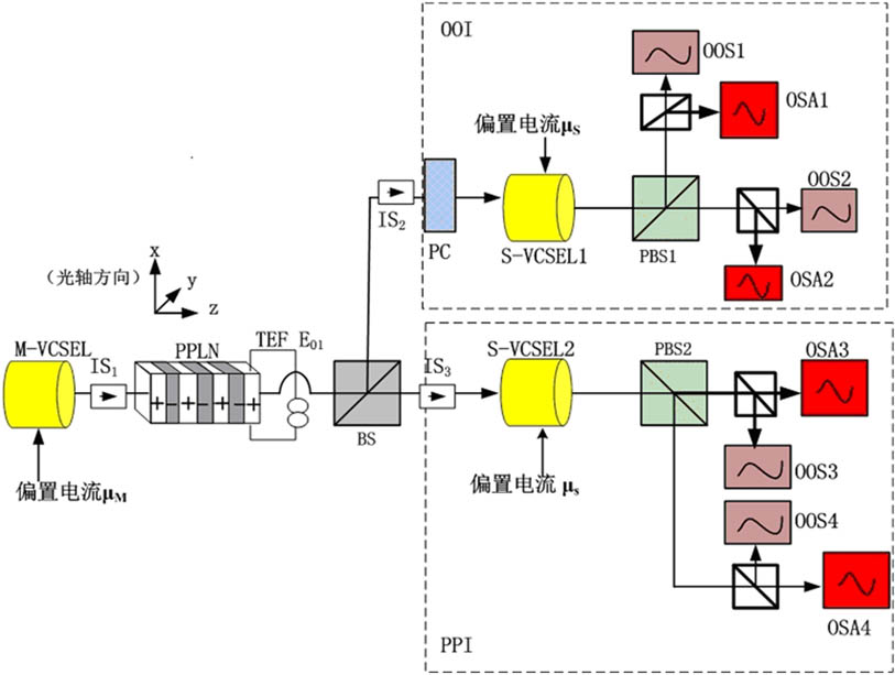
The control scheme of the PS and NDBs of an optically injected VCSEL is displayed in Fig. 1, where we have noted the transverse electric field (TEF); isolator 1 () is used to avoid the light from the left side of the PPLN to feedback into the M-VCSEL; and and ensure that the output light from the right-hand side of the PPLN propagates to the S-VCSEL1 and the S-VCSEL2 unidirectionally, respectively. The applied electric field is used for EO intensity modulation. The M-VCSEL subject to a certain bias current injection emits two LP mode components, i.e., TE and TM modes, which are along the - and -direction of the coordinate axis of the crystal, respectively. Consequently, they are defined as the - and -LP component, respectively. With the applied to the PPLN crystal, the two LP components experience EO modulation. The modulated light is divided into two light beams by a beam-splitter (BS). The - and -LP of one are first converted into - and -LP by a polarization controller (PC), and are then injected into S-VCSEL1. Consequently, this laser is subject to OOI. The two LP components of the other are directionally injected into S-VCSEL2. As a result, the laser is subjected to POI. The temporal traces of the - and -LP component emitted by S-VCSEL1 are measured by optical oscilloscopes (OOSs) 1 and 2, respectively. Optical spectrum analyzers (OSAs) 1 and 2 are used to test the power spectrums of these two LP components. The time traces of the two LP components of the S-VCSEL2 are measured by OOSs 3 and 4, respectively. The corresponding power spectrums are tested by OSAs 3 and 4.
Figure 1.Schematic of the control scheme for the PS and the NDBs of optically injected VCSEL.
According to SFM[2], the rate equations of M-VCSEL subject to the bias current injection are as where the subscript means the M-VCSEL; the subscripts and indicate the - and -LP components, respectively; is the complex amplitude of the optical field; and , respectively, are the total carrier concentration and difference in concentration between carriers with spin-up and spin-down; , where the photon lifetime in the solitary VSCEL cavity; a is the linewidth enhancement factor; is the spin relaxation; is the nonradiative carrier relaxation rate; and are the dichroism and birefringence, respectively; is the spontaneous-emission rate; and are two independent complex Gaussian white noise events with zero mean and 1 variance. Suppose that the - and -LP components are considered as the original input of the o- and e-light in the crystal; the dependence of the complex amplitude of the two independent polarization components on of the two LP components are as[7]where is Planck’s constant; the effective area of the light spot; is the volume of the active layer in the laser; C is the light velocity in vacuum; is the round trip time of light in the laser cavity; is the length of laser cavity; is the effective refractive index of the active layer; is the central frequency of the laser pulse emitted by the M-VCSEL; and are the undisturbed refractive of the - and -LP, respectively; is the delay of the light propagating from the M-VCSEL to the S-VCSEL. The other second-order nonlinear effects are very weak and are neglected due to phase mismatch. The wave-coupling equations of the linear EO effect for two LP components in a PPLN crystal are obtained, as[16]The effective EO coefficients are where , , , 2, 3 (the same throughout the paper); and are the diagonalized electric permittivity tensor elements; are the EO tensor elements; and are the unit vectors of o- and e-light, respectively; is the unit vector of the applied electric field; and in a uniaxial crystal of PPLN; and are the polar angle and the azimuth angle, respectively; ; and ; is a zero-order Fourier coefficient; and are positive and negative first-order Fourier coefficients, respectively. The duty ratio , where and are the length of the positive and that of negative domain, respectively. The wave vector mismatch , is the first-order reciprocal lattice vector, and is the poled period of the crystal. Additionally, and are the wave vector of the - and -LP component at , respectively; and is the wave vector of light in vacuum. Here, we consider close to the wave vector mismatch , and neglect those components that make little contributions to the EO effect because of phase mismatch.
While the two LP components subject to EO modulation are injected into S-VCSEL1 or S-VCSEL2, their amplitudes become Consequently, the rate equations of S-VCSEL2 subject to POI are[2,3–7]where is the difference between the central frequency of M-VCSEL and that of S-VCSEL. Suppose that S-VCSEL1 is the same as S-VCSEL2; there is a slight difference between the rate equations of S-VCSEL2 and those of S-VCSEL, owing to the S-VCSEL1 subject to OOI. For S-VCSEL1, the last term for optical injection in Eq. (13) should be modified as .
To describe the polarization of the S-VCSEL, we define the polarization degree of the light pulse as follows where the symbol indicates the mean value; ; . The subscripts 1 and 2 show the S-VCSEL1 and the S-VCSEL2, respectively. The PD ranges between and 1. shows that the output of the slave VCSEL is the -LP mode; for , the output is the -LP mode; if , it is CP mode; it is right-handed EP mode when ; it is left-handed EP mode for . First, we numerically calculate the rate equations [Eqs. (1)–(3) and (13)–(15)] by the four-order Rung–Kutta method. The data in calculation are given in Table 1, where and come from the Shellmeier formula for a PPLN crystal[19]. To facilitate the discussion, the spontaneous emission noise terms in Eqs. (1) and (13) are ignored in the numerical calculation of the following, owing to the slight influence it has on the PS of the laser[20]. The parameter values of system for calculation are as follows. ; ; ; ; ; ; ; ; ; ; ; ; ; ; ; ; ; ; ; . The EO tensor elements are ; ; ; .
For different bias current of M-VCSEL, we calculate the dependence of of the output light from S-VCSEL2 with POI on the applied electric field , shown in Fig. 2. Here, ; ; ; . In Fig. 2, one sees that for any , the appears to be a change of periodic oscillation with the applied electric field . The period is . In addition, the oscillates between and 1. The envelope cure of its oscillating peak is the cosine curve, and that of its oscillating wave trough is the sine curve. From Fig. 2, we obtain the PS law of the output light of the S-VCSEL2 in one period of change when the is fixed at 1.048 (Fig. 3). From Fig. 3, one sees that the output polarization is first switched from the original -LP into left-handed EP, then undergoes five cycles of conversion among the left-handed EP, the CP and the right-handed EP, and finally is switched into the original -LP. For , the PS rule of the output in an oscillating period is given in Fig. 4. As seen from Fig. 4, with the fixed at , the initial polarization emitted by the S-VCSEL2 is the left-handed EP. With the increase in the , the output polarization is switched into the CP, then experiences four cycles of switching between CP, the right-handed EP, and the left-handed EP. Once again, it becomes the CP. Finally, it is restored to the original left-handed EP. Also we give the PS rule of the output in one period of oscillating change when is fixed at 1.18 (Fig. 5). From Fig. 5, it is found that the output polarization is switched from the original -LP into the right-handed EP. Then it undergoes the following five cycles of PS: the right-handed left-handed EP. It finally becomes the original -LP again. Under the same condition, for different bias current , we also calculate the dependence of the output polarization from S-VCSEL1 with OOI on the applied electric field . One sees from Fig. 6 that under the same condition of original polarization, the PS law of the output light from S-VCSEL1 with OOI is nearly the same as that from S-VCSEL2 with POI in one change period of the . But under the same and , compared with the case of the salve VCSEL subjected POI, the output polarization state has changed, i.e., , , left-handed EP and right-handed EP, when the salve VCSEL is subjected to OOI.
Figure 2.For different bias current of M-VCSEL, the dependence of the output of light from S-VCSEL2 with POI on the applied electric field , where , , and . Blue-line: ; red-line: ; green-line: .
Figure 6.For different bias current of the M-VCSEL, the dependence of the output of light from S-VCSEL1 with OOI on the applied electric field , where , , and . Blue-line: ; red-line: ; green-line: .
Here we take as an example to calculate the temporal traces of the light intensities of the two LP mode components of the S-VCSEL2 output (Fig. 7). From Fig. 7, it is found that the output of the S-VCSEL2 is the -LP mode component, and the temporal trajectories of its light intensity show period-doubling when [Fig. 7(a)].With the increase of the to , the temporal traces of each LP component of the laser output are nearly the same and the output is the CP mode. However, the temporal traces of each LP component appear to be a chaotic orbit [Fig. 7(b)]. For , the output is the -LP mode component and the temporal traces are quasi-period [Fig. 7(c)]. When the is further increased to , the output is restored to the -LP mode component, but the temporal trajectories become chaos. Figure 8 gives further the temporal traces of the light-intensity of each LP component from S-VCSEL1 subject to OOI, where the parameters are the same as that in Fig. 7. From Fig. 8, one sees that when the is taken as 0, 0.6849, 1.325, and in turn, the output of the laser in turn becomes the -LP, the CP mode, the -LP, and the -LP. The temporal traces of the output show period-doubling, chaos, quasi-period, and chaos in turn.
Figure 7.Under different the applied electric field , the temporal traces of the light intensity of the output - or -LP mode component from S-VCSEL2 with POI when , , , and . Here, blue-line: x-LP; red-line: y-LP. (a) , (b) , (c) , and (d) .
Figure 8.Under different the applied electric field , the temporal traces of the light intensity of the output - or -LP mode component from S-VCSEL1 with OOI when , , , and . Here, blue-line: x-LP; red-line: y-LP. (a) , (b) , (c) , and (d) .
We present a novel manipulation scheme for PS and NDBs of an optically injected laser system composed of M-VCSEL and S-VCSEL. Here, the PS and the NDBs of the S-VCSEL can be effectively and steadily controlled when the light from the master VCSEL subject to EO modulation. From the aforementioned results, it is concluded that the output polarization of the slave VCSEL subject to POI or OOI shows a variation of periodic oscillation with the applied TEF. The envelope trajectories of its oscillation peak take on a cosine curve, and that of its oscillation wave trough appears to be a sine curve. With the bias current of the master VCSEL fixed at a certain value, the slave VCSEL can emit arbitrary polarization mode and generate different NDBs evolutions by EO modulation. These results have potential applications in some focused scientific fields, such as the exploration of a controllable optical composite logic gate based on the polarization characteristic of VCSELs, the multi-channel encryption system based on polarization-division-multiplexing.
Dongzhou Zhong. Control of the polarization switching and the nonlinear dynamic behaviors of vertical cavity surface-emitting lasers with external optical injection[J]. Chinese Optics Letters, 2015, 13(Suppl.): S21405