
Cizhe Fang, Qiyu Yang, Qingchen Yuan, Xuetao Gan, Jianlin Zhao, Yao Shao, Yan Liu, Genquan Han, Yue Hao. High-Q resonances governed by the quasi-bound states in the continuum in all-dielectric metasurfaces[J]. Opto-Electronic Advances, 2021, 4(6): 200030-1
- Opto-Electronic Advances
- Vol. 4, Issue 6, 200030-1 (2021)
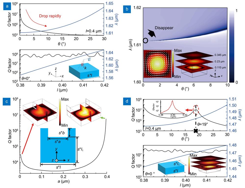
Fig. 1. (a ) Simulated Q factor and resonant wavelength as a function of θ (top) and l (bottom), respectively. Inset: the schematic view of the model (a square block with l =0.4 μm). (b ) Simulated transmission spectrum as a function of the angle and wavelength. Inset: the magnetic field profiles under the normal incidence condition, where white arrows correspond to electric field vectors and the black wireframe outlines the single unit. (c ) Modeled the Q factor as a function of a for a broken-symmetry square block (l =0.4 μm). Bottom inset: the schematic image of the concave Si block. The top two insets show the magnetic field distributions at around a =0 μm and a =0.4 μm, respectively. (d ) Simulated Q factor and resonant wavelength as a function of θ (top) and l (bottom) for the BIC mode at a =0.4 μm. The top inset: simulated Q factor as a function of l at θ =19°. The bottom left inset: the schematic view of the model (a rectangle block with l 1=0.3 μm). The bottom right inset: the magnetic field profile at θ =0°. The scaling parameter is set as 1.2 in (a−d).
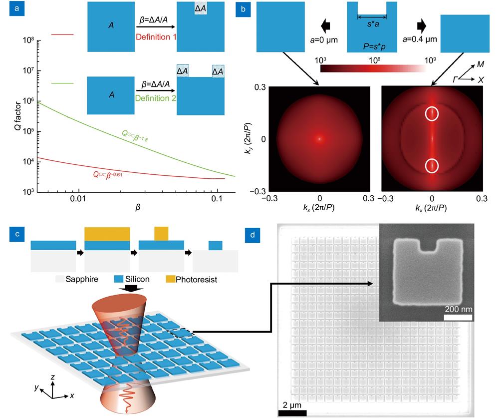
Fig. 2. (a ) Dependence of the Q factor on asymmetry parameter β for both designs (log-log scale). Inset: two definitions of the asymmetry parameter. (b ) Simulated Q in momentum space at a =0 μm (left) and a =0.4 μm (right). Inset: the designed patterns shown in the xy plane for both cases. (c ) Schematic image of a period metasurface with concave nanopillars. Inset: device fabrication process. (d ) SEM image of the fabricated metasurface.
Fig. 3. (a ) Measured transmission spectrum at different s (20×20 array). Inset: The magnetic field distribution in the yz plane for the metasurface with the substrate. (b ) Polarization dependence measurements of the transmission (T exp) and reflection (R exp) spectra at a wavelength of 1.55 μm and their corresponding calculations (i.e. T sim and R sim). The arrow indicates the direction of the x -axis. (c ) Top: Modeled the calculated and measured Q factor as a function of a (s =1.2 and b =0.1 μm). Inset: SEM image of the single unit at a =0.02 μm and a =0.32 μm, respectively. Bottom: The evolution of Q factor at different α for two definitions (log-log scale). (d ) Numerically simulated dependence of the resonant wavelength and Q factor on t sub (t sub=0 μm means that there is no substrate). The top inset shows the comparison of the measured Q factor for different dimensions and array sizes. Structure 1: l =0.4 μm, a =0.15 μm, b =0.1 μm, and s =1.15. Structure 2: l =0.5 μm, a =0.1 μm, b =0.1 μm, and s =1.02. The bottom inset shows the SEM images of the prepared structures before and after the process optimization.
Fig. 4. Magnitude plots of the on-resonance magnetic field for the isolated resonator and 3×3, 5×5, 7×7, and 9×9 arrays. The magnetic field distributions are obtained at the vertical mid-plane of the blocks and the magnitude is indicated by the height. The structural parameters are l =0.4 μm, a =0.15 μm, b =0.1 μm, s =1.2. The table on the right shows the corresponding Q factors.
Fig. 5. (a ) Measured transmission spectrum of the proposed metasurface (200×200 array) and its fitting of Fano function. Optimized structural parameters are p =0.6 μm, l =0.5 μm, a =0.1 μm, b =0.1 μm, s =1.05. (b ) Comparison of THG in the proposed structure (red line) and a flat Si film with the same thickness (black line). The intensity of the THG in the flat Si film is amplified 100 times. (c ) The electric field profiles at the resonance (left) and the off-resonance (right), respectively. (d ) The corresponding polarization dependence measurements (normalized to the peak value of the resonance).


Set citation alerts for the article
Please enter your email address

© Copyright 2018-2021 | Chinese Laser Press. All Rights Reserved 沪ICP备15018463号-20