• Journal of Inorganic Materials
  • Vol. 38, Issue 3, 329 (2023)
Zhiqiang WANG1, Ji’an WU1, Kunfeng CHEN1、*, and Dongfeng XUE2、*
Author Affiliations
  • 11. Institute of Novel Semiconductors, State Key Laboratory of Crystal Materials, Shandong University, Jinan 250100, China
  • 22. Multiscale Crystal Materials Research Center, Shenzhen Institute of Advanced Technology, Chinese Academy of Sciences, Shenzhen 518055, China
  • show less
    DOI: 10.15541/jim20220646 Cite this Article
    Zhiqiang WANG, Ji’an WU, Kunfeng CHEN, Dongfeng XUE. Large-size Er,Yb:YAG Single Crystal: Growth and Performance[J]. Journal of Inorganic Materials, 2023, 38(3): 329 Copy Citation Text show less
    Characteristics of as-grown Er,Yb:YAG single crystal and wafer(a) With diameter of 80 mm and length of 230 mm; (b) Wafer with a thickness of 1.5 mm; (c) XRD patterns for wafer and ground powder; (d) EDS pattern of the wafer
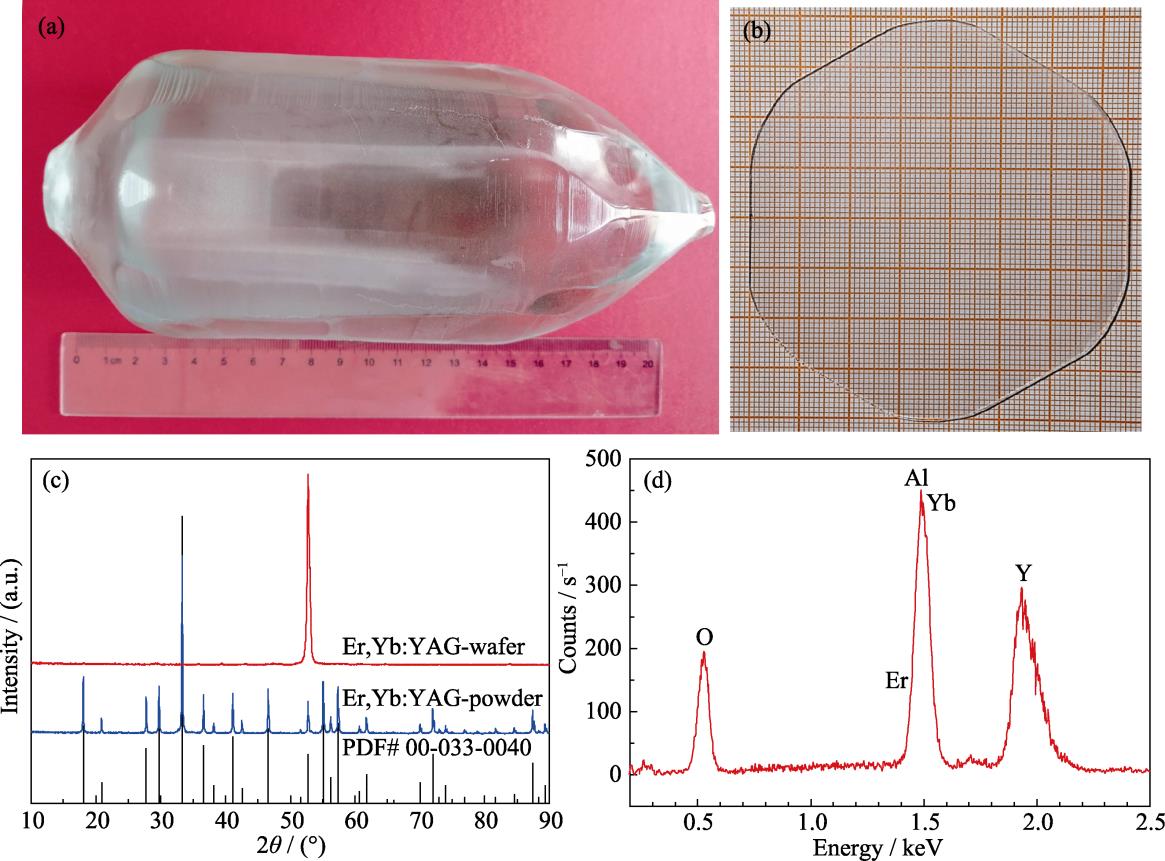
    1. Characteristics of as-grown Er,Yb:YAG single crystal and wafer(a) With diameter of 80 mm and length of 230 mm; (b) Wafer with a thickness of 1.5 mm; (c) XRD patterns for wafer and ground powder; (d) EDS pattern of the wafer
    Micrographs of wafer surface with (111) face(a, b) Before etching; (c, d) Etched in H3PO4 at 180 ℃ for 60 min
    2. Micrographs of wafer surface with (111) face(a, b) Before etching; (c, d) Etched in H3PO4 at 180 ℃ for 60 min
    Raman spectrum of Er,Yb:YAG
    3. Raman spectrum of Er,Yb:YAG
    Raman spectra of different points at Er,Yb:YAG wafer(a) Five points on a straight line; (b) Peak positions and FWHM obtained by Lorentz fitting at the 783 cm-1 band with nisets showing Er,Yb:YAG wafer and schematic diagram of Raman test points
    4. Raman spectra of different points at Er,Yb:YAG wafer(a) Five points on a straight line; (b) Peak positions and FWHM obtained by Lorentz fitting at the 783 cm-1 band with nisets showing Er,Yb:YAG wafer and schematic diagram of Raman test points
    Optical absorption spectra of Er,Yb:YAG crystal in the range of 200-1050 nm at room temperature
    5. Optical absorption spectra of Er,Yb:YAG crystal in the range of 200-1050 nm at room temperature
    Emission spectra of Er,Yb:YAG crystal at room temperature(a) Excited by 382 nm; (b) Excited by 260 nm; Fluorescent decay curves of (c) 554 nm; (d) 405 nm emission; Colorful figures are available on website
    6. Emission spectra of Er,Yb:YAG crystal at room temperature(a) Excited by 382 nm; (b) Excited by 260 nm; Fluorescent decay curves of (c) 554 nm; (d) 405 nm emission; Colorful figures are available on website
    Wavelength/nmAssignment (from ground 4I15/2)
    2554D7/2
    3562K15/2
    3642G9/2
    3814G11/2
    4072H9/2
    4424F3/2
    4504F5/2
    4884F7/2
    518, 5242H11/2
    5424S3/2
    647, 6554F9/2
    7884I9/2
    961, 9664I11/2
    Table 1.

    Correspondence between the experimentally observed absorption lines and energy levels of Er3+ in Er,Yb:YAG single crystal[11,33 -36]

    Zhiqiang WANG, Ji’an WU, Kunfeng CHEN, Dongfeng XUE. Large-size Er,Yb:YAG Single Crystal: Growth and Performance[J]. Journal of Inorganic Materials, 2023, 38(3): 329
    Download Citation