We theoretically and experimentally demonstrate an RGB achromatic metalens that operates concurrently at three visible wavelengths (, 532, and 700 nm) with a high numerical aperture of 0.87. The RGB metalens is designed by simple integration of metalens components with the spatial interleaving method. The simulated spatial interleaving metalens shows RGB achromatic operation with focusing efficiencies of 25.2%, 58.7%, and 66.4% at the wavelengths of 450, 532, and 700 nm, respectively. A 450 μm diameter metalens operating at three designated wavelengths is fabricated with low-loss hydrogenated amorphous silicon. The fabricated metalens has the measured focusing efficiencies of 5.9%, 11.3%, and 13.6% at , 532, and 700 nm, respectively. The Strehl ratios of 0.89, 0.88, and 0.82 are obtained at given wavelengths, which show a capability of diffraction-limited operation.
1. INTRODUCTION
Metasurfaces based on subwavelength scale structures have emerged as a next-generation optical platform for enabling complete control of the properties of light [1–31]. Depending on the geometrical parameters and materials of the designed nanostructures, known as meta-atoms, various metasurfaces that manipulate visible light have been proposed, such as metaholograms [1–11], plasmonic resonators [12–14], phase control devices [15–19], and compact photonic devices [20–31]. All-dielectric metalenses have received great attention in particular, due to having various industrial applications [32–39] and advantages over traditional lenses such as their ultrathin compact integration, multifunctionality [32–35], and high numerical aperture (NA) imaging [36–39] in the visible spectrum.
However, as with conventional refractive lenses, chromatic dispersion is a limiting factor for metalenses, which means that existing all-dielectric metalenses can be operated only by one specific design wavelength. Recently, several methods have been introduced to reduce chromatic dispersion such as control of the group delay dispersion of light by adjusting the geometric parameters and rotation angle of nanofins [40,41]. Chromatic dispersion can be reduced by compensating the optical path difference to the focus of the transmitted light for different wavelengths through the variation of group delay dispersion of nanofins. However, they have an NA of less than 0.2, making them unsuitable for high-resolution imaging systems. Various metalenses have also been demonstrated [42,43] but have NAs of less than 0.3 and do not operate at visible wavelengths. Multilayer stacking and spatial multiplexing have also been reported for achromatic metalenses operating at several discrete wavelengths [44–50]. Multilayer stacking can be demonstrated by Fresnel zone plates or independent phase modulation at different wavelengths [43,44]. However, these metalenses have low efficiency due to noise between stacked metasurfaces. Because of this problem, various metalenses have been integrated into one metalens by spatial multiplexing [46–49]. These metalenses can operate at two [46,47] or three [48,49] discrete wavelengths but are still limited due to low NA (). Such problems can be solved by the spatial integration of different isotropic meta-atoms. The simple integration of isotropic meta-atoms based on unit cell engineering can increase the operating wavelengths of the metalens. Therefore, this method can reduce chromatic dispersion.
Here, we propose a polarization-insensitive RGB achromatic metalens by spatial integration of three distinct meta-atoms to design a metalens that operates at three wavelengths in the visible spectrum (450, 532, and 700 nm). The meta-atoms for two wavelengths (532 and 700 nm) are embedded in the metalens designed to operate at the wavelength of 450 nm. To design a high NA and high-efficiency metalens, dielectric meta-atom transmitter arrays composed of low-loss hydrogenated amorphous silicon (a-Si:H) are used [50]. By controlling the hydrogenation and silicon disorder, a-Si:H is optimized to provide a near-zero extinction coefficient () in the visible spectrum. Also, it has a higher refractive index than conventional materials such as titanium dioxide (), gallium nitride (GaN), or silicon nitride (SiN). This leads to higher efficiency metalenses than previous results in our group using [51]. The calculated efficiencies of the a-Si:H-based spatial interleaving method (SIM) metalens are 25.2%, 58.7%, and 66.4% at the wavelengths of 450, 532, and 700 nm, respectively. Furthermore, the metalens is successfully fabricated by using simple plasma-enhanced chemical vapor deposition (PECVD) and electron-beam lithography (EBL) processes. The fabricated metalens has with a diameter of 450 μm and measured efficiencies of 5.9%, 11.3%, and 13.6% at , 532, and 700 nm, respectively.
Sign up for Photonics Research TOC. Get the latest issue of Photonics Research delivered right to you!Sign up now
2. RESULTS AND DISCUSSION
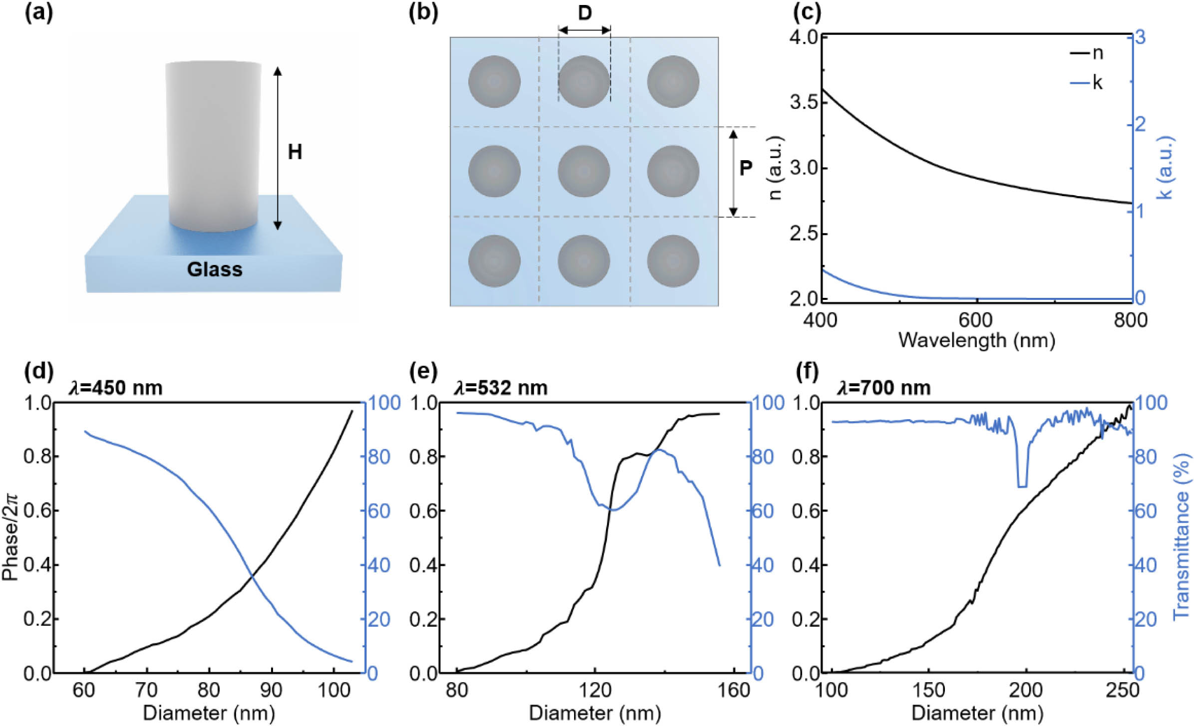
To design an RGB achromatic metalens operating at three discrete wavelengths, the following hyperbolic phase profile must be satisfied to prevent spherical aberration [52]: where is the radial distance from the center, is the incident wavelength of light, and is the designed focal length. For polarization-insensitive operation, circular meta-atoms on glass substrate are used [Fig. 1(a)]. To realize the required phase profile , the geometrical parameters such as diameter (D) and height (H) are optimized to provide full phase coverage from 0 to [Fig. 1(b)]. As D increases, the phase of the transmitted light is modulated from 0 to , showing that the full phase coverage can indeed be achieved. A sufficiently high H is also required for full phase coverage, as the phase change increases when the length of the optical path increases. In addition, since a proper lattice constant (P) is required for high efficiency, transmitted light must be restricted to only the 0th order. This can be predicted by the grating equation at normal incidence as given by , where is the refractive index of the medium, is diffraction order, and is the th diffraction angle. When high-order diffraction occurs (i.e., ), the transmitted light cannot be focused. Therefore, a sufficiently small P is required to avoid anomalous scattering. To achieve the required phase profile with the following considerations, low-loss a-Si:H is used for meta-atoms [50]. It has a higher refractive index () than or SiN and a lower extinction coefficient () than conventional silicon-based materials in the visible spectrum [Fig. 1(c)]. Sufficiently high of a-Si:H makes it suitable for achieving full phase coverage at low height.
Figure 1.(a) Schematic image of a low-loss hydrogenated amorphous silicon (a-Si:H) meta-atom on a glass substrate. (b) Top view of metalens building blocks with a rectangular array. (c) Measured refractive index and extinction coefficient of low-loss a-Si:H. (d)–(f) Simulated phase and transmittance for meta-atoms as a function of diameter (D) at , (e) 532, and (f) 700 nm. ; for ; for and 700 nm.
Taking these considerations into account, finite-difference time-domain (FDTD) simulations were conducted to optimize the geometrical parameters (D, H, and P) of the meta-atoms and to calculate their transmission properties (see Appendix A). The transmitted phase can be adjusted from 0 to by varying D from 60 to 104 nm at [Fig. 1(d)]. Full phase coverage was also obtained at and for and 700 nm, respectively [Figs. 1(e) and 1(f)]. The meta-atoms have been optimized by and at . For and 700 nm, optimized P was 460 nm with the same H. Full phase coverage also can be achieved at with high transmittance, resulting in a high aspect ratio (AR). However, high AR and small diameter of meta-atom () reduce the feasibility of the fabricated metalens due to a limitation of resolution in EBL; therefore, the H was set to be 600 nm (see Appendix A). In addition, was optimized to meet the 0th-order diffraction condition of the grating equation and the Nyquist sampling criterion () for high transmittance (see Appendix A). At , does not satisfy the Nyquist sampling criterion but was used to simplify the interleaving process. The transmittance of the meta-atoms at gradually decreases with increasing D due to the nonzero of a-Si:H.
To realize the RGB achromatic operation of metalens at three wavelengths (450, 532, and 700 nm), SIM is applied to three distinct meta-atoms. Three metalenses for , 532, and 700 nm can be integrated by substituting one of four blue meta-atoms with red meta-atoms and, likewise, one of two red meta-atoms with green meta-atoms [Fig. 2(a)]. The light transmitted from the meta-atoms at each wavelength can constructively interfere at the focus when the coupling between neighboring meta-atoms is weak.
Figure 2.(a) Schematic illustrations of spatial interleaving method with three meta-atoms: , 532, and 700 nm for blue, green, and red circles, respectively. (b) Simulated cross-sectional normalized electric field distributions of the metalens at (top), 532 nm (middle), and 700 nm (bottom) in the focal region. (c)–(e) Calculated normalized electric field distributions at the focal spot at , (d) 532 nm, and (e) 700 nm. Scale bar: 500 nm.
To theoretically investigate the focusing properties of an RGB achromatic metalens, the cross-sectional electric-field (E-field) distributions in the focal region with different incident wavelengths of light () are calculated using 3D finite-difference time-domain (3D FDTD) simulations (see Appendix A). The designed metalens has a diameter μ, μ, and . The transmitted light with , 532, and 700 nm is focused at through the SIM metalens [Fig. 2(b)]. The focusing efficiency is calculated by the ratio of optical power at the focal spot to the total incident power on the metalens. Focusing efficiencies of 25.2%, 58.7%, and 66.4% are calculated at , 532, and 700 nm, respectively. The normalized E-field distributions of the SIM metalens at μ confirm that the two metalenses focus the incident light at the almost same spot for , 532, and 700 nm [Figs. 2(c) to 2(e)]. The focusing efficiency at is slightly lower than at and 700 nm because of the absorption by nonzero of a-Si:H. Additionally, the focusing efficiency decreases as decreases due to the phase difference of meta-atoms at three different wavelengths. For , the meta-atoms have , which is relatively small for ; thus, the phase error due to the meta-atoms of is small when the SIM metalens operates at . However, when the metalens operates at 450 or 532 nm, a large phase error can be caused by the meta-atoms for . In addition, high-order diffraction () can occur at and 532 nm due to the large diameter of meta-atoms for .
The fabricated metalens has μ, μ, and , which is the same NA as the simulated metalens [Figs. 3(a) and 3(b); see Appendix B]. To investigate the focusing properties of the fabricated SIM metalens, we measured the intensity profile in the focal plane for various propagation distances in the -direction using a custom-built setup [Fig. 3(c); see Appendix C]. The focal spot of the plane was determined by taking the location of the maximum intensity. The cross-sectional images were combined to produce the optical field intensity profile along the axis [Fig. 3(d)]. The transmitted light with , 532, and 700 nm through the fabricated metalens was focused at , which is consistent with the simulation results.
Figure 3.(a), (b) Scanning electron micrograph of the fabricated metalens for (a) top-down and (b) tilted SEM images. (c) Schematic illustration of the optical setup. (d) Normalized measured optical field intensity profiles at (top), 532 nm (middle), and 700 nm (bottom).
The point spread function of the metalens at three incident wavelengths (, 532, and 700 nm) was measured at each focal spot [Figs. 4(a)–4(c)]. The focusing efficiency of fabricated metalens is defined as the ratio of optical power at the focal spot to the total incident power. Focusing efficiencies of 5.9%, 11.3%, and 13.6% were measured at , 532, and 700 nm, respectively. In addition, focusing efficiencies were measured depending on the polarization to confirm the polarization-insensitive characteristic of the SIM metalens (see Appendix D). These are lower than the simulated results, but the trends are similar. It can be improved through further research (see Appendix E). To compare the SIM metalens and the perfect lens, measured intensity profiles and their Airy functions were plotted and normalized at each wavelength [Figs. 4(d) to 4(f)]. The normalized intensity of the Airy function is given as follows [53]: where is the maximum intensity, and is the Bessel function of the first order. The measured FWHMs of the SIM metalens were 298.5, 323.4, and 457.1 nm at , 532, and 700 nm, respectively. Diffraction-limited FWHMs at the respective incident wavelengths, derived from the Airy function (i.e., ), are 264.6, 312.8, and 411.6 nm. The measured FWHMs of the SIM metalens are comparable with Airy functions, implying that the fabricated metalens is diffraction-limited. To confirm this, the Strehl ratios (SRs), which are the figure of merit to indicate the imaging quality of the lens, are calculated by normalizing and integrating the ideal Airy functions and measured intensity profiles to obtain the power of the lens. After that, we multiply a compensating factor, so that the calculated powers of the metalens and perfect lens are the same. Finally, we calculate the SR by dividing the central intensity of the Airy function and measured profile [54]. SRs of 0.89, 0.88, and 0.82 were obtained at , 532, and 700 nm, respectively. Considering that the maximum value of SR is 1, the high enough SR value at each wavelength represents excellent imaging performance of the metalens. Therefore, the fabricated SIM metalens is capable of diffraction-limited operation. Compared with the existing RGB metalens study, the SIM metalens has a high resolution (low FWHM value) and a sufficiently high Strehl ratio value with a high NA (Appendix F).
Figure 4.(a)–(c) Captured image of the focal spot created by the metalens at , (b) 532 nm, and (c) 700 nm. (d)–(f) Normalized cross-sectional intensity profiles and Airy functions at , (e) 532 nm, and (f) 700 nm. (g)–(i) MTF of the metalens at , (h) 532 nm, and (i) 700 nm.
To characterize the optical system in the spatial frequency domain, the modulation transfer function (MTF) through the Fourier transform relation was obtained [Figs. 4(g)-4(i)]. It is the standard resolution, indicating how the image is blurred by using the lens. We calculated MTF values from three wavelength cases from the equation below [55]: where is the pupil function from the experimentally obtained focusing images, and and are the spatial frequency of the and coordinates, respectively. The high spatial frequency value in MTF means that fine patterns are also possible, and the image can be resolved above the cutoff frequency, which is the point where the MTF value decreases to 0. From the MTF result, sharp drops of MTF are shown at all wavelengths, and it can be interpreted that the shorter wavelength light has a better resolution ability.
Also, we confirmed the imaging capabilities of the metalens by using a negative 1951 USAF target (Thorlabs R3L1S4N). The imaging macroscopy setup is shown in Fig. 5(a). The laser light was cropped by a pinhole to adjust it to the proper size and was incident on a negative resolution target. An objective lens (Olympus PLN10X) ensured the diverging light with a wide area of target images focused tightly on metalens. The resulting images were captured with the CCD camera. The image of the resolution target was successfully captured at [Fig. 5(b)]. However, in the case of blue light (), the imaging efficiency is low; in the case of red light (), the intensity of the supercontinuum laser is weak, so the imaging results could not be captured by CCD camera and sCMOS camera.
Figure 5.(a) Experimental setup for imaging setup. (b) Captured image of a negative 1951 USAF resolution target using the SIM metalens at .
The achromatic imaging of the SIM metalens was investigated by using a screen-capture system [Fig. 6(a)]. The image reflected on the screen was taken with the camera. Since the metalens is a high NA lens with an NA of about 0.87, the screen had to be close. Therefore, the magnified image was large (as large as several cm) even if the system was used. The same number “5” of the resolution target was compared for each wavelength [Fig. 6(b)]. Even though the images were not clear compared with Fig. 5, and there were some distortions because of the limit of the oblique screen-capture system, the SIM metalens demonstrated the capability of achromatic imaging.
Figure 6.(a) Screen-capture system in bright and dark conditions. (b) Captured image of the same number “5” at , 532, and 700 nm.
In summary, we successfully designed and experimentally realized an RGB achromatic metalens operating at three wavelengths in the visible spectrum. The spatial interleaving method is used to demonstrate the RGB achromatic metalens by the simple spatial integration of meta-atoms. This method yields a metalens (μ, μ, and ) that focuses light of , 532, and 700 nm with calculated efficiencies of 25.2%, 58.7%, and 66.4%, respectively. The fabricated metalens achieves focusing efficiencies of 5.9%, 11.3%, and 13.6% at the given wavelengths. This efficiency loss was caused by fabrication error, but it can be improved by further optimization during the fabrication process. We also demonstrated that our fabricated metalens is capable of diffraction-limited operation. The spatial interleaving method could be further generalized to multifunctional metasurfaces at specific wavelengths or RGB achromatic operation of more than three wavelengths. Furthermore, RGB achromatic metalenses working at discrete wavelengths have the potential for applicability in various display devices such as CMOS image sensors, which are essential for next-generation display technology.
Acknowledgment
Acknowledgment. J.R. acknowledges an industry-academia strategic grant funded by Samsung Display Co., Ltd. Y.K. acknowledges the Hyundai Motor Chung Mong-Koo fellowship, and the NRF fellowships (NRF-2022R1A6A3A-13066251 and NRF-2022K1A3A1A12080445), respectively, funded by the Ministry of Education and the Ministry of Science and ICT of the Korean government. J.K. acknowledges the POSTECH Alchemist fellowship.
APPENDIX A: SIMULATION
FDTD simulation was used for the numerical analysis of the meta-atoms. The simulation tool was an electromagnetic calculation module (RSoft FullWAVE) from commercial software RSoft 2014.09 (Synopsys and RSoft Design Group, Inc.). The simulation structure consists of a low-loss a-Si:H of 600 nm and glass substrate () of 1 μm. The thickness of the glass substrate was reduced to 1 μm to prevent time consumption for the FDTD simulation. The refractive index and extinction coefficient of a-Si:H [50] and [56] were taken from the literature. A plane wave with a given is excited from the glass substrate to the a-Si:H meta-atoms. For the realization of the polarization insensitivity of meta-atoms, 50% transverse electric (TE) and 50% transverse magnetic (TM) modes are averaged. Perfectly matched layers (PMLs) were used at the top and bottom boundaries to avoid the occurrence of the reflected electromagnetic waves at the edge of the structure, and periodic boundary conditions were used to describe a uniform array of meta-atoms of a given diameter and periodicity. The mesh grid size was set to 10 nm. All simulations were conducted until a steady state was reached (i.e., variation of the electric field is per FDTD time step).
The focusing characteristics of the metalens were calculated by using the 3D FDTD method. The same light source was used, and all boundary conditions were set to PML. To obtain the spatial electric field distribution, the monitor was set to discrete Fourier transform (DFT) mode. The grid size was set to 20 nm for the metalens to reduce the simulation time.
Based on the following simulation setup, the phase and transmittance of meta-atoms were calculated according to the variation of and [Figs. 7(a) and 7(b)]. Full-phase coverage was obtained at , so the was set to 600 nm to reduce the aspect ratio of meta-atoms. In the next step, the phase and transmittance were calculated at according to the period change at , 532, and 700 nm [Figs. 8(a) to 8(f)]. The black lines were set as the region that satisfies full-phase coverage and high transmittance of meta-atoms while avoiding anomalous diffraction.
Figure 7.Simulated transmission properties of the meta-atoms of , at . (a) Phase. (b) Transmittance. The period was set to 230 nm, which satisfies the Nyquist sampling criteria. Black lines: optimized structures used in this work to achieve full-phase coverage with high efficiency.
Figure 8.Simulated (a) phase and (b) transmittance of the meta-atoms of , at . Simulated (c) phase and (d) transmittance of the meta-atoms of , at . Simulated (e) phase and (f) transmittance of the meta-atoms of , at . The H is set to 600 nm, which is the optimization result in Fig. 7. Black lines: optimized structures used in this work to achieve full-phase coverage with high transmittance while avoiding anomalous diffraction.
A 600 nm thick layer of a-Si:H film was deposited on the glass substrate PECVD. A positive electron beam resist (Microchem, 950 PMMA A2) was spin-coated on the film at 2000 r/min, and then baked at 180°C for 5 min. The resist was exposed using EBL (ELS-7800, ELIONIX). The exposed photoresist was developed in methyl isobutyl ketone/isopropyl alcohol 1:3 solution. Then, a 40 nm thick chromium (Cr) layer was deposited on the sample using electron beam evaporation; then, the sample was immersed in acetone for 1 min with sonication for a lift-off process. The Cr was used as an etch mask for the a-Si:H in an inductively coupled plasma reactive ion etching (ICP-RIE) process. The remaining Cr etch mask was removed using Cr etchant.
APPENDIX C: CHARACTERIZATION OF THE FOCUSING PERFORMANCE OF THE METALENS
Considering the target wavelength of our metalens, we used CW diode laser (CPS450 from Thorlabs for 450 nm and CPS532 from Thorlabs for 532 nm) and supercontinuum laser (SC-Pro-7 from YSL for 700 nm) as illuminators. To characterize the focusing properties of the metalens, we measured the intensity profile in the focal plane along the direction with 0.5 μm intervals. A schematic of the optical setup is shown in Fig. 3(c). The microscope characterizing setup consists of an objective lens (Olympus LMPLFLN ) and a CCD camera (Lumenera INFINITY2-2), which are on the motorized stage. To estimate focusing efficiency, we measured the power in the focal spot (the power of transmitted light passing through a circular area with a radius of four times the FWHM) divided by the incident light power with a power meter (PM120VA from Thorlabs).
APPENDIX D: POLARIZATION-INSENSITIVE OPERATION
To investigate the polarization-insensitivity of the SIM metalens, the focusing efficiency is measured depending on the polarization of incident light by using a custom-built setup [Fig. 9(a)]. As a representative, the focusing efficiency is measured using the blue laser (). In the linear polarization cases, we added a half-wave plate (HWP) to rotate the linearly polarized light in an intentional direction. A quarter-wave plate (QWP), in which the fast axis is at an angle of 45° to the linear polarizer, is added for the circular polarization. Even if the polarization of incident light changes, the focusing efficiency exhibits a small variation (average , standard deviation ) [Fig. 9(b)]. These differences are small enough to establish the polarization-insensitivity of the SIM metalens.
Figure 9.(a) Schematic image of the custom-built setup for efficiency measurement depending on the polarization. (b) Measured focusing efficiency of the SIM metalens according to polarization variation.
The calculated focusing efficiency of the SIM metalens is 25.2% at and 58.7% and 66.4% at and 700 nm, respectively. Low-loss a-Si:H, which is used in our metalens, has a nonzero at () and near-zero at and 700 nm. This is an optimized result to provide the lowest in the visible spectrum. However, since the bandgap of silicon (1.12 eV) is too small, absorption at is inevitable. Therefore, the focusing efficiency decreases due to the absorption by a-Si:H at . The focusing efficiency at can be improved by using a material with a large bandgap (), such as GaN or .
The measured focusing efficiencies of the SIM metalens, 5.9% at , 11.3% , and 13.6% are all lower than the calculated values. These differences can be induced by fabrication defects [57]. The most critical defect is a tilted sidewall [Fig. 3(b)]. To investigate the effect of the tilted sidewall, the phase and transmittance of slanted nanopillars are calculated by FDTD simulation (Fig. 10). The slanted meta-atom with tilted angle is used for simulation [Fig. 10(a)]. With slanted meta-atoms, full phase coverage cannot be achieved for the same diameter range as in Fig. 1 [Figs. 10(b)–10(d)]. Because of these discrepancies, some of the transmitted light cannot be focused at the focal spot, reducing focusing efficiency. This kind of defect can be corrected through optimization of the ICP-RIE process.
Figure 10.(a) Schematic image of slanted meta-atom on the glass substrate. (b)–(d) Simulated phase for slanted meta-atoms as a function of at , (c) 532, and (d) 700 nm. Height ; for ; for and 700 nm. , 3.5°, and 4.5° for , 532, and 700 nm, respectively.
Table 1 presents the comparison of our lenses with previous achromatic or RGB metalenses. We did not include achromatic lenses that were only simulated, only lenses that were fabricated and measured. This table shows that our RGB metalens has a high resolution (low FWHM value) and a sufficiently high Strehl ratio value with a high NA value compared with the existing RGB metalens study.