• Chinese Optics Letters
  • Vol. 17, Issue 2, 020005 (2019)
Tian Jiang1、2、3、*, Runlin Miao1, Jie Zhao1, Zhongjie Xu1, Tong Zhou2, Ke Wei1, Jie You4, Xin Zheng4, Zhenyu Wang4, and Xiang'ai Cheng1
Author Affiliations
  • 1College of Advanced Interdisciplinary Studies, National University of Defense Technology, Changsha 410073, China
  • 2State Key Laboratory of High Performance Computing, College of Computer, National University of Defense Technology, Changsha 410073, China
  • 3Interdisciplinary Center of Quantum Information, National University of Defense Technology, Changsha 410073, China
  • 4National Institute of Defense Technology Innovation, Academy of Military Sciences PLA China, Beijing 100010, China
  • show less
    DOI: 10.3788/COL201917.020005 Cite this Article Set citation alerts
    Tian Jiang, Runlin Miao, Jie Zhao, Zhongjie Xu, Tong Zhou, Ke Wei, Jie You, Xin Zheng, Zhenyu Wang, Xiang'ai Cheng. Electron–phonon coupling in topological insulator Bi2Se3 thin films with different substrates[J]. Chinese Optics Letters, 2019, 17(2): 020005 Copy Citation Text show less
    (a) AFM image of the high-quality Bi2Se3 film. It is grown on the p-type Si (111) substrate, which is highly doped by boron, by using the MBE under a base vacuum ∼1.0 × 10⁻¹⁰ Torr. (b) XRD pattern of Bi2Se3 film after subtracting the signal from the p-type Si (111) substrate. (c) and (d) RHEED patterns of the Bi2Se3 film grown on the Si (111) substrate along the [112¯] (Γ–M) and [11¯0] (Γ–K) directions, respectively. (e) Room temperature Raman spectrum of eight QL Bi2Se3 thin film.
    Fig. 1. (a) AFM image of the high-quality Bi2Se3 film. It is grown on the p-type Si (111) substrate, which is highly doped by boron, by using the MBE under a base vacuum 1.0×10¹⁰Torr. (b) XRD pattern of Bi2Se3 film after subtracting the signal from the p-type Si (111) substrate. (c) and (d) RHEED patterns of the Bi2Se3 film grown on the Si (111) substrate along the [112¯] (ΓM) and [11¯0] (ΓK) directions, respectively. (e) Room temperature Raman spectrum of eight QL Bi2Se3 thin film.
    (a) TR spectrum acquired with 1.78–3.04 eV probe energy. (b) The reflection change for probe energy levels at three white dashed lines of (a).
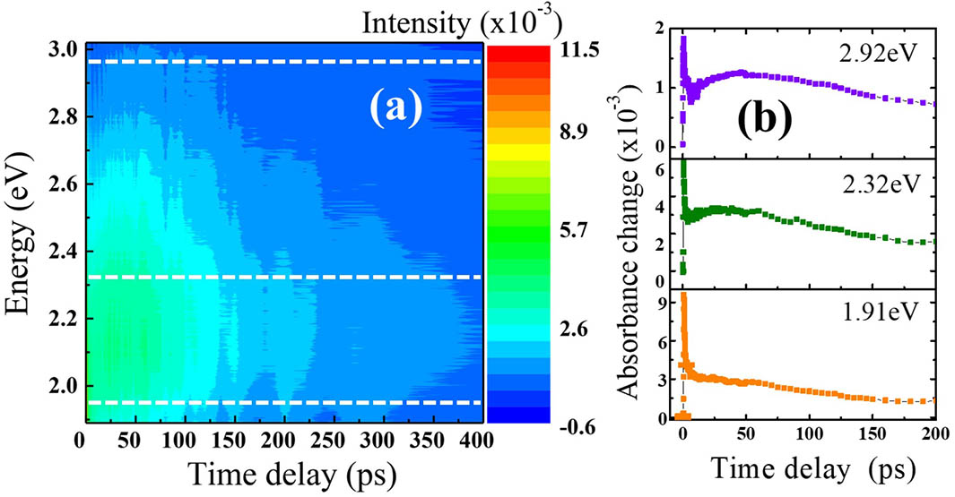
    Fig. 2. (a) TR spectrum acquired with 1.78–3.04 eV probe energy. (b) The reflection change for probe energy levels at three white dashed lines of (a).
    (a) TR trace acquired at 2.32 eV, which is divided into four parts. (b) The energy spectrum plotted as a function of amplitude. (c) The schematic diagram of the pump and probe processes.
    Fig. 3. (a) TR trace acquired at 2.32 eV, which is divided into four parts. (b) The energy spectrum plotted as a function of amplitude. (c) The schematic diagram of the pump and probe processes.
    (a) TR spectrum of eight QL Bi2Se3 thin films grown on the STO substrate. (b) TR spectrum of eight QL Bi2Se3 thin films grown on the Al2O3 substrate.
    Fig. 4. (a) TR spectrum of eight QL Bi2Se3 thin films grown on the STO substrate. (b) TR spectrum of eight QL Bi2Se3 thin films grown on the Al2O3 substrate.
    (a) Amplitude changes linearly with the increasing pump fluence. (b) The TR traces of samples grown on Al2O3 (black line) and STO (blue line) substrates extracted at the probe energy of 2.32 eV.
    Fig. 5. (a) Amplitude changes linearly with the increasing pump fluence. (b) The TR traces of samples grown on Al2O3 (black line) and STO (blue line) substrates extracted at the probe energy of 2.32 eV.
    Tian Jiang, Runlin Miao, Jie Zhao, Zhongjie Xu, Tong Zhou, Ke Wei, Jie You, Xin Zheng, Zhenyu Wang, Xiang'ai Cheng. Electron–phonon coupling in topological insulator Bi2Se3 thin films with different substrates[J]. Chinese Optics Letters, 2019, 17(2): 020005
    Download Citation