Author Affiliations
1College of Advanced Interdisciplinary Studies, National University of Defense Technology, Changsha 410073, China2State Key Laboratory of High Performance Computing, College of Computer, National University of Defense Technology, Changsha 410073, China3Interdisciplinary Center of Quantum Information, National University of Defense Technology, Changsha 410073, China4National Institute of Defense Technology Innovation, Academy of Military Sciences PLA China, Beijing 100010, Chinashow less
Abstract
Broadband transient reflectivity traces were measured for thin films with various substrates via a 400 nm pump–white-light-probe setup. We have verified the existence of a second Dirac surface state in and qualitatively located it by properly analyzing the traces acquired at different probe wavelengths. Referring to the band structure of , the relaxation mechanisms for photo-excited electrons with different energies are also revealed and studied. Our results show a second rise of the transient reflection signal at the time scale of several picoseconds. The types of substrate can also significantly affect the dynamics of the rising signal. This phenomenon is attributed to the effect of lattice heating and coherent phonon processes. The mechanism study in this work will benefit the fabrication of high-performance photonic devices based on topological insulators.Three-dimensional (3D) topological insulators (TIs), a rather fresh quantum state of matter, could exhibit an insulating bulk state and a robust conductive surface state (SS) simultaneously[1–5]. The unique electronic structure of TIs leads to tremendous intriguing physical phenomena under light excitation, making TIs potential candidates for future opto-electronic and opto-spintronic applications[6–11]. Thus, it is essential to explore the non-equilibrium properties of TIs under light excitation, such as phonon, carrier, as well as spin dynamics of both the SS and the bulk. The relaxation mechanism of photo-excited hot carriers has been intensively studied by various methods, including the optical pump optical probe (OPOP)[12–19], optical pump terahertz probe (OPTP)[20–23], time-resolved angle-resolved photoemission spectroscopy (Tr-ARPES)[24–28], Raman spectroscopy[29,30], second harmonic generation (SHG)[31–33], as well as the time-resolved Kerr rotation (TRKR)[31,34].
Despite the relevant studies and some convincing explanations for the relaxation path of electrons, there are some issues that remain obscure. Most of the transient reflection (TR) traces were studied by using a two-color pump–probe system, which can reveal the relaxation process of photo-excited carriers at a certain energy level[12–17]. However, there is a great need to study the relaxation process of electrons excited to different energy levels. In addition, the existence of a second Dirac SS has been previously reported, which is located at 1.5–2.5 eV above the Fermi level[26,27]. Thus, it would be appealing and beneficial to investigate not only different relaxing behaviors of the photo-excited electrons located at both the second Dirac SS and the bulk conduction bands (CBs), but also the coupling effects between the second SS (2nd SS) and the bulk states.
In this Letter, transient reflectivity measurements are employed to investigate the photo-excited carrier dynamics in the prototypical 3D TI via a 400 nm pump and white-light-probe system. The relaxation information of electrons in different regions of the energy band is acquired by adjusting the probe wavelength. The second Dirac SS of is revealed by properly analyzing the transient spectrum. Furthermore, a second rise of TR signal is observed for films grown on different substrates.
Sign up for Chinese Optics Letters TOC. Get the latest issue of Chinese Optics Letters delivered right to you!Sign up now
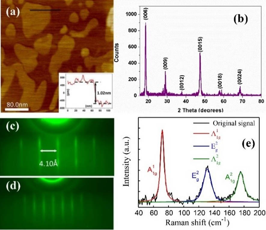
The sequence of Se–Bi–Se–Bi–Se forms a stack or quintuple layer (QL) along the -axis direction of the rhombohedral structure. Each QL is approximately 1 nm thick. In this Letter, the single crystal with eight QLs was grown on -type silicon (Si) (111), , and (STO) substrates by using a custom-made molecular beam epitaxy (MBE) system under a base vacuum (1 Torr = 133.322 Pa). The bismuth source with 99.9999% purity and selenium source with 99.999% purity were thermally evaporated from Knudsen cells to provide stable fluxes. Reflection high-energy electron diffraction (RHEED) was used to monitor the crystal quality and crystal structure of thin films during growth. Figures 1(c) and 1(d) show the RHEED patterns of the film grown on the Si (111) substrate along the [] and [] directions, respectively. The clear and sharp diffraction streaks indicate high crystalline quality and flat surface morphology of the film. From the positions of the streaks relative to the Si (111) substrate (, 1 Å = 0.1 nm), we deduce the lattice constant of the epitaxy film to be 4.10 Å, which is in good agreement with the values reported previously. To confirm the crystalline structure of the MBE grown films, we employ X-ray diffraction (XRD), with the results of 8 nm film shown in Fig. 1(b). The sharp diffraction peaks (006), (009), (0012), (0015), (0018), and (0024) from film can be obviously seen. Notably, the XRD pattern of our film shows that only (003)-type lattice planes own the QL thickness of 0.98 nm, which is consistent with the atomic force microscopy (AFM) measured step height [Fig. 1(a)]. Hence, the good quality of the rhombohedral film is well supported by the AFM, XRD, and RHEED characterizations.
![(a) AFM image of the high-quality Bi2Se3 film. It is grown on the p-type Si (111) substrate, which is highly doped by boron, by using the MBE under a base vacuum ∼1.0 × 10⁻¹⁰ Torr. (b) XRD pattern of Bi2Se3 film after subtracting the signal from the p-type Si (111) substrate. (c) and (d) RHEED patterns of the Bi2Se3 film grown on the Si (111) substrate along the [112¯] (Γ–M) and [11¯0] (Γ–K) directions, respectively. (e) Room temperature Raman spectrum of eight QL Bi2Se3 thin film.](/Images/icon/loading.gif)
Figure 1.(a) AFM image of the high-quality film. It is grown on the -type Si (111) substrate, which is highly doped by boron, by using the MBE under a base vacuum . (b) XRD pattern of film after subtracting the signal from the -type Si (111) substrate. (c) and (d) RHEED patterns of the film grown on the Si (111) substrate along the [] () and [] () directions, respectively. (e) Room temperature Raman spectrum of eight QL thin film.
Furthermore, Fig. 1(e) presents the Raman spectrum of the eight QL thin film. Here, the black curve is experimental data and the other ones are three Lorentzian–Gaussian fitting curves. We unambiguously assign the peak at to the shear phonon mode, and the other two peaks located at and are assigned to the and longitudinal phonon modes, respectively. The peak positions match very well with the previous studies on thin films[29,30], which further verifies good quality of the sample.
Our TR spectra are acquired by a typical pump–probe system, where the 400 nm femtosecond pump pulse is focused onto the sample with a fluence of . The induced reflection changes are recorded by a white-light continuum probe pulse with a tunable time delay to the pump pulse. Detailed information of our experiment setup can be found in the previous works of our group[19,35].
The TR spectrum of eight-layer films with the Si substrate acquired at the probe energy between 1.78 and 3.02 eV (411–697 nm) is shown in Fig. 2(a), in which the recombination processes detected at different probe wavelengths are changing gradually. In order to have a better view of the signals in the time domain, we extract the signals at three different probe energies, as marked by the white dashed lines in Fig. 2(a), the results being shown in Fig. 2(b). The responsible region of the energy band for the different probe lights is marked in Fig. 3(c).
Figure 2.(a) TR spectrum acquired with 1.78–3.04 eV probe energy. (b) The reflection change for probe energy levels at three white dashed lines of (a).
Figure 3.(a) TR trace acquired at 2.32 eV, which is divided into four parts. (b) The energy spectrum plotted as a function of amplitude. (c) The schematic diagram of the pump and probe processes.
We zoomed in the TR trace acquired at 2.32 eV and divided the signal into four parts, as shown in Fig. 3(a). Particularly, in the period of , the carrier excitation and thermalization processes occur, with the corresponding sketch being shown in Fig. 3(c). The characteristic time remains around 300 fs no matter how the probe energy changes. However, the amplitudes of the signals are quite different when measured at different probe wavelengths by the end of . According to former researches[8,9,12], the excited charge carriers would affect the reflection signal of via two mechanisms, namely, the free-carrier absorption (weak due to indirect absorption) and the phase-space filling (dominant). From our pump–probe data acquired with different pump fluence at the probe energy of 2.07 eV [as shown in Fig. 4(a)], it is clear that the amplitude changes linearly with the pump fluence in the range of . It is already proved that the reflection change () is proportional to the carrier density when the sample is not saturated[36]. According to previous angle-resolved photoemission spectroscopy (ARPES) results[25–27], the excited carriers will relax to states near the Fermi level within about 1 ps. As a result, the amplitude of the band filling effect is mainly determined by the density of holes and the density of states (DOS) at the corresponding energy levels. Since the hole density is the same for different probing energies, the peak value of the TR signal at different probing energies is approximately proportional to the DOS. By plotting probe energy as a function of amplitude A, the DOS in the different energy levels range is thus revealed, with the result shown in Fig. 3(b). Based on some previous studies on ARPES[25–27], a 2nd SS is observed between 1.5 and 2.5 eV above the Fermi level, as shown in Fig. 3(c). A clear relationship between Figs. 3(b) and 3(c) is derived. To start with, we can divide the curve in Fig. 3(b) into three parts. The first part illustrates that the energy band is more filled with the decreasing probe energy, which could be related to the second CB, followed by a decrease of amplitude due to the coexistence of the bulk band and SS in part 2. Moreover, the amplitude oscillation in the last part is possibly induced by the 2nd SS. Additionally, we did not observe the Dirac point of the 2nd SS due to the limit of the probe energy range. Thus, the results prove that the position and shape of the 2nd SS of can be qualitatively characterized via a simple pump–probe experiment.
Figure 4.(a) TR spectrum of eight QL thin films grown on the STO substrate. (b) TR spectrum of eight QL thin films grown on the substrate.
Figure 5.(a) Amplitude changes linearly with the increasing pump fluence. (b) The TR traces of samples grown on (black line) and STO (blue line) substrates extracted at the probe energy of 2.32 eV.
In order to explore the influence of different substrates, we performed pump–probe experiments on two other eight QL films that are grown on STO and substrates with the same experiment system. The results of the reflectance change () are shown in Fig. 5. It is obvious that the reflectance change spectrum is quite different from the sample grown on the Si substrate (Fig. 2), especially the second rise behavior of the signal. For convenience of comparison, we extract the signals of the two samples at the probe energy of 2.32 eV, as shown in Fig. 4.
Compared with the results shown in Fig. 2, the signals for different substrates show similar dynamics, except in time region , where all signals show a second rise, but are quite different in time scales and amplitudes. The second rise phenomena are attributed to the effects of carrier–phonon interactions, such as coherent acoustic phonons and lattice heating. For the samples grown on and STO substrates (Fig. 4), the second rise appears at around the time delay of 5 ps with only a slight difference. While for the sample grown on Si (Fig. 2), the second rise appears at the time delay of 50 ps, which is quite different from the other two substrates. These differences are probably due to the different carrier lifetimes in different samples. For samples grown on and STO substrates, the carriers are not likely to transfer from because of the large band gap of and STO. The carriers have short lifetimes in the films. On the other hand, the promising carrier transfer between and Si substrates results in much larger carrier lifetimes and thus a longer second rising time scale. Another difference is the amplitude of the second rise. Comparing Figs. 2 and 4, it is easy to see that the second rise is strongest on the STO substrate, probably due to its larger thermal expansion coefficients. The second rise is much weaker on Si and substrates. Thus, we tend to attribute the second rise on Si to the electron and phonon interaction between the sample and substrate due to the time scale, while we assume the weak second rise on the substrate is caused by the coherent acoustic phonon, based on previous reports[8,19]. These results, together with some former studies[37], should be useful for future applications of TI thin films.
In conclusion, we found that the TR change spectroscopy acquired with white probe light is connected to the DOS of material. Thus, the pump–probe experiment qualitatively verified the existence of 2nd SS in the conductive band of . Moreover, we performed the same pump–probe experiment on 3 eight QL thin films grown on different substrates, Si, , and STO. The results show that the second rise behavior is quite different on different substrates. For thin film grown on Si, the second rise is possibly caused by the electron and phonon interaction between the sample and substrate. Due to the large thermal expansion coefficients of STO, the second rise is rather strong on this substrate. Compared to other two-dimensional (2D) materials [such as transition metal dichalcogenides (TMDCs) and perovskites], TI films have more significant phonon effects, such as coherent phonon and lattice heating effects.
References
[1] C. L. Kane, E. J. Mele. Science, 314, 1692(2006).
[2] J. E. Moore. Nat. Phys., 5, 378(2009).
[3] J. E. Moore. Nature, 464, 194(2010).
[4] X. L. Qi, S. C. Zhang. Phys. Today, 63, 33(2010).
[5] M. Z. Hasan, C. L. Kane. Rev. Mod. Phys., 82, 3045(2010).
[6] Z. Wang, H. Mu, J. Yuan, C. Zhao, Q. Bao, H. Zhang. IEEE J. Sel. Top. Quantum Electron., 23, 8800105(2017).
[7] Q. Wang, Y. Chen, L. Miao, G. Jiang, S. Chen, J. Liu, X. Fu, C. Zhao, H. Zhang. Opt. Express, 23, 7681(2015).
[8] K. Yin, B. Zhang, L. Li, X. Zhou, T. Jiang, J. Hou. Photon. Res., 3, 72(2015).
[9] C. Zhao, Y. Zou, Y. Chen, Z. Wang, S. Lu, H. Zhang, S. Wen, D. Tang. Opt. Express, 20, 27888(2012).
[10] D. Sun, M. Wang, Y. Huang, Y. Zhou, M. Qi, M. Jiang, Z. Ren. Chin. Opt. Lett., 15, 051603(2017).
[11] P. Tang, Y. Tao, Y. Mao, M. Wu, Z. Huang, S. Liang, X. Chen, X. Qi, B. Huang, J. Liu, C. Zhao. Chin. Opt. Lett., 16, 020012(2018).
[12] J. L. Wang, L. Guo, C. H. Liu, X. Xu, Y. F. Chen. Appl. Phys. Lett., 107, 063107(2015).
[13] J. L. Wang, L. Guo, C. Ling, Y. Song, X. Xu, Z. Ni, Y. Chen. Phys. Rev. B, 93, 155306(2016).
[14] S. Kim, D. H. Shin, J. H. Kim, C. W. Jang, J. W. Park, H. Lee, S. H. Choi, S. H. Kim, K. J. Yee, N. Bansal, S. Oh. Nanotechnology, 27, 045705(2015).
[15] Y. D. Glinka, S. Babakiray, T. A. Johnson, A. D. Bristow, M. B. Holcomb, D. Lederman. Appl. Phys. Lett., 103, 151903(2013).
[16] Y. D. Glinka, S. Babakiray, T. A. Johnson, M. B. Holcomb, D. Lederman. J. Appl. Phys., 117, 165703(2015).
[17] Y. D. Glinka, S. Babakiray, T. A. Johnson, M. B. Holcomb, D. Lederman. Appl. Phys. Lett., 105, 171905(2014).
[18] D. Panna, R. Marjieh, E. Sabag, L. Rybak, A. Ribak, A. Kanigel, A. Hayat. Appl. Phys. Lett., 110, 212103(2017).
[19] J. Zhao, Z. J. Xu, Y. Y. Zang, Y. Gong, X. Zheng, K. He, X. A. Cheng, T. Jiang. Opt. Express, 25, 14635(2017).
[20] S. Sim, M. Brahlek, N. Koirala, S. Cha, S. Oh, H. Choi. Phys. Rev. B, 89, 165137(2014).
[21] V. S. Kamboj, A. Singh, T. Ferrus, H. E. Beere, L. B. Duffy, T. Hesjedal, C. H. W. Barnes, D. A. Ritchie. ACS Photon., 4, 2711(2017).
[22] P. Le, P. Liu, C. Luo, J. Lin, K. Wu. J. Alloys Compd., 692, 972(2017).
[23] Y. G. Choi, C. J. Zhung, S. H. Park, J. Park, J. S. Kim, S. Kim, J. Park, J. S. Lee. Phys. Rev. B, 97, 075307(2018).
[24] Y. Zhang, K. He, C. Chang, C. Song, L. Wang, X. Chen, J. Jia, Z. Fang, X. Dai, W. Shan, S. Shen, Q. Niu, X. Qi, S. Zhang, X. Ma, Q. Xue. Nat. Phys., 6, 712(2010).
[25] J. A. Sobota, S. Yang, J. G. Analytis, Y. L. Chen, I. R. Fisher, P. S. Kirchmann, Z. X. Shen. Phys. Rev. Lett., 108, 117403(2012).
[26] J. A. Sobota, S. L. Yang, A. F. Kemper, J. J. Lee, F. T. Schmitt, W. Li, R. G. Moore, J. G. Analytis, I. R. Fisher, P. S. Kirchmann, T. P. Devereaux, Z. X. Shen. Phys. Rev. Lett., 111, 136802(2013).
[27] J. A. Sobota, S. L. Yang, D. Leuenberger, A. F. Kemper, J. G. Analytis, I. R. Fisher, P. S. Kirchmann, T. P. Devereaux, Z. X. Shen. J. Electron Spectrosc. Relat. Phenom., 195, 249(2014).
[28] R. Heid, I. Y. Sklyadneva, E. V. Chulkov. Sci. Rep., 7, 1095(2017).
[29] C. Wang, X. Zhu, L. Nilsson, J. Wen, G. Wang, X. Shan, Q. Zhang, S. Zhang, J. Jia, Q. Xue. Nano Res., 6, 688(2013).
[30] J. Zhang, Z. Peng, A. Soni, Y. Xiong, B. Peng, J. Wang, M. S. Dresselhaus, Q. Xiong. Nano Lett., 11, 2407(2011).
[31] D. Hsieh, F. Mahmood, J. W. McIver, D. R. Gardner, Y. S. Lee, N. Gedik. Phys. Rev. Lett., 107, 077401(2011).
[32] J. W. McIver, D. Hesieh, S. G. Drapcho, D. H. Torchinsky, D. R. Gardner, Y.S. Lee, N. Gedik. Phys. Rev. B, 86, 035327(2012).
[33] Y. D. Glinka, S. Babakiray, T. A. Johnson, M. B. Holcomb, D. Lederman. Phys. Rev. B, 91, 195307(2015).
[34] M. C. Wang, S. Qiao, Z. Jiang, S. N. Luo, J. Qi. Phys. Rev. Lett., 116, 036601(2016).
[35] K. Wei, X. Zheng, X. Cheng, C. Shen, T. Jiang. Adv. Opt. Mater., 4, 1993(2016).
[36] R. Wang, B. A. Ruzicka, N. Kumar, M. Z. Bellus, H. Y. Chiu, H. Zhao. Phys. Rev. B, 86, 045406(2012).
[37] Y. Chen, C. J. Zhao, S. Q. Chen, J. Du, P. H. Tang, G. B. Jiang, H. Zhang, S. C. Wen, D. Y. Tang. IEEE J. Sel. Top. Quantum Electron., 20, 315(2014).