• Photonics Research
  • Vol. 9, Issue 7, 1182 (2021)
Ahmed E. Hassanien*, Steffen Link, Yansong Yang, Edmond Chow, Lynford L. Goddard, and Songbin Gong
Author Affiliations
  • Holonyak Micro and Nanotechnology Laboratory, Department of Electrical and Computer Engineering, University of Illinois at Urbana-Champaign, Urbana, Illinois 61801, USA
  • show less
    DOI: 10.1364/PRJ.421612 Cite this Article Set citation alerts
    Ahmed E. Hassanien, Steffen Link, Yansong Yang, Edmond Chow, Lynford L. Goddard, Songbin Gong. Efficient and wideband acousto-optic modulation on thin-film lithium niobate for microwave-to-photonic conversion[J]. Photonics Research, 2021, 9(7): 1182 Copy Citation Text show less
    (a) Mock-up of the proposed AO modulator concept; (b) simulated average strain on 1 μm wide 560 nm thick optical WG; (c) total refractive index variation, in principal directions, due to simulated strain in (b).
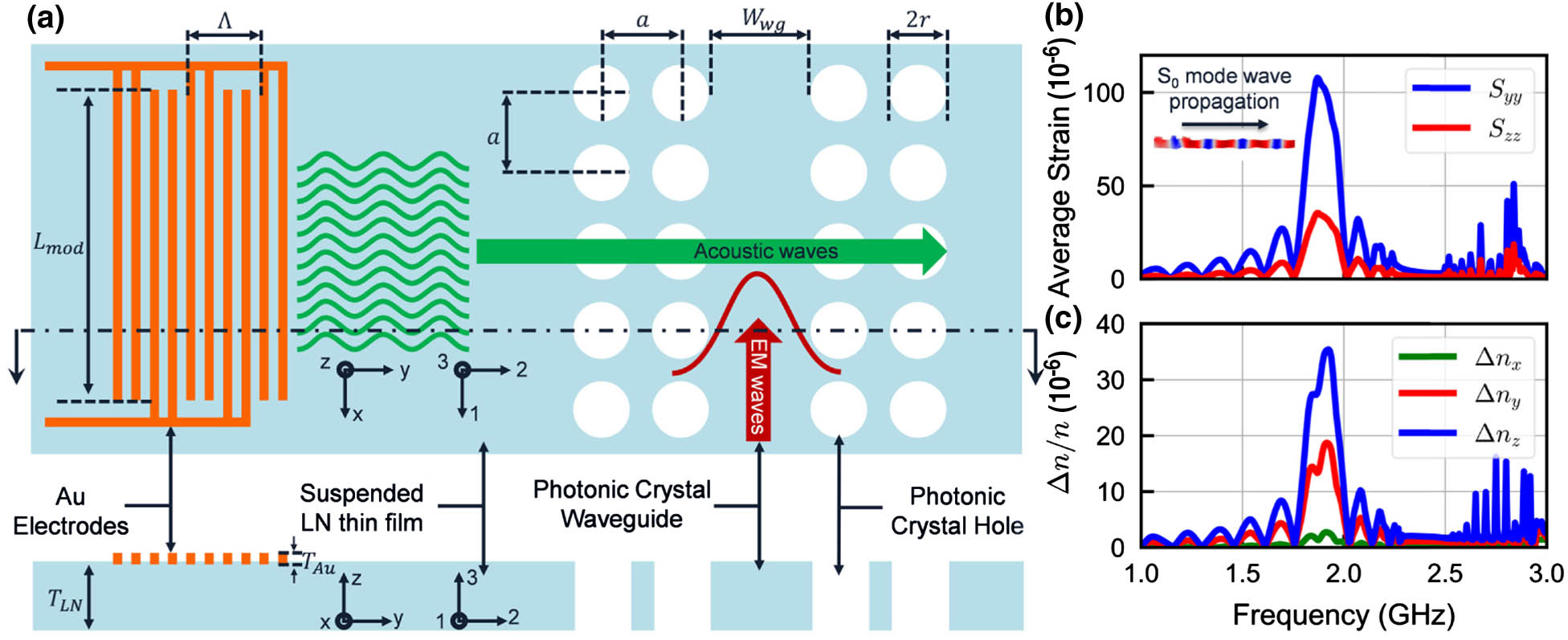
    Fig. 1. (a) Mock-up of the proposed AO modulator concept; (b) simulated average strain on 1 μm wide 560 nm thick optical WG; (c) total refractive index variation, in principal directions, due to simulated strain in (b).
    (a) Microscope image of the fabricated MZI; (b) measurement setup for the optical response of the MZI device. EDFA, erbium-doped fiber amplifier; FPC, fiber polarization controller; DUT, device under test; DAQ, data acquisition card. (c) Measured optical response of the MZI; (d) cross-sectional SEM image of the optical WG (left) and simulated TM mode shape, including WG sidewalls (right).
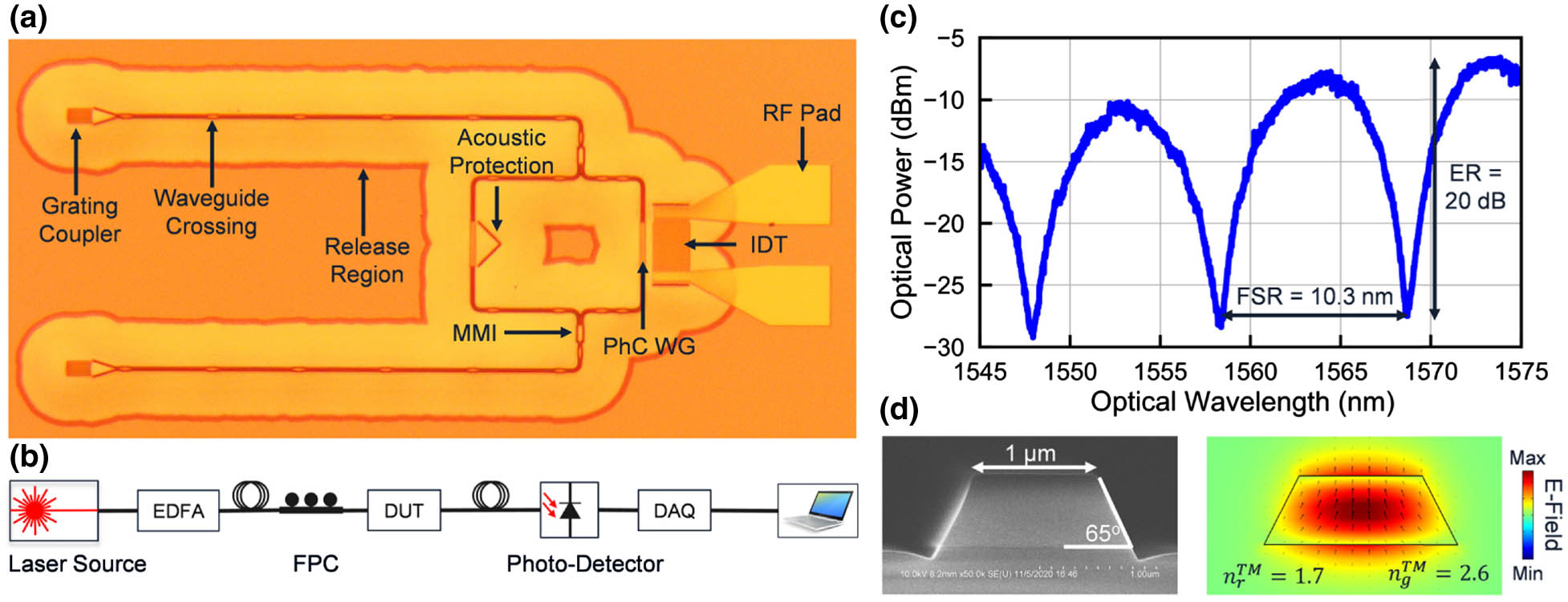
    Fig. 2. (a) Microscope image of the fabricated MZI; (b) measurement setup for the optical response of the MZI device. EDFA, erbium-doped fiber amplifier; FPC, fiber polarization controller; DUT, device under test; DAQ, data acquisition card. (c) Measured optical response of the MZI; (d) cross-sectional SEM image of the optical WG (left) and simulated TM mode shape, including WG sidewalls (right).
    (a) Fabrication process. BOX, buried oxide; PR, photoresist. SEM images of (b) IDTs and modulated MZI arm; (c) PhC WG; (d) etched region used to protect the unmodulated MZI arm from the acoustic waves; (e) zoomed-in IDTs; (f) zoomed-in IDTs and PhC WG; and (g) WGC used for mechanical tethering.
    Fig. 3. (a) Fabrication process. BOX, buried oxide; PR, photoresist. SEM images of (b) IDTs and modulated MZI arm; (c) PhC WG; (d) etched region used to protect the unmodulated MZI arm from the acoustic waves; (e) zoomed-in IDTs; (f) zoomed-in IDTs and PhC WG; and (g) WGC used for mechanical tethering.
    (a) Measurement setup; (b) measured optical powers versus wavelength for device A; (c) measured S-parameters of device A at optical wavelength of 1561 nm.
    Fig. 4. (a) Measurement setup; (b) measured optical powers versus wavelength for device A; (c) measured S-parameters of device A at optical wavelength of 1561 nm.
    (a) Measured S-parameters of device B at optical wavelength of 1560.6 nm; (b) measured S-parameters of device C at optical wavelength of 1558.5 nm; (c) SEM image of device C.
    Fig. 5. (a) Measured S-parameters of device B at optical wavelength of 1560.6 nm; (b) measured S-parameters of device C at optical wavelength of 1558.5 nm; (c) SEM image of device C.
    DeviceNIDTΛ (μm)Lmod (μm)a (μm)Wwg (μm)r (×a)TLN (μm)TAu (nm)
    A252.9450.710.350.5650
    B492.9450.710.350.5650
    C72.8450.710.350.5650
    Table 1. Fabricated Devices’ Dimensions
    Ref./DeviceAcoustic CavityFrequency (GHz)BW (MHz)Qap (rad/mW)Lmod (μm)ap/Lmod [rad/(mWmm)]VπL (V·cm)PπL (mW·cm)Mismatch Efficiencya (%)
    [20]0.110.06218000.07312000.0612.5b22242
    [18]3.270.936000.271002.70.0461.3564
    [37]0.110.0912000.2624000.110.943595
    [24]c0.520.073154.82.77
    [25]c0.520.131201.087
    C1.160.4824000.5445120.0190.1519.3
    A×1.90140140.0166450.370.3816150
    B×1.9070270.0175450.390.27145.390
    Table 2. Performance Summary and Comparison to SoA
    Ahmed E. Hassanien, Steffen Link, Yansong Yang, Edmond Chow, Lynford L. Goddard, Songbin Gong. Efficient and wideband acousto-optic modulation on thin-film lithium niobate for microwave-to-photonic conversion[J]. Photonics Research, 2021, 9(7): 1182
    Download Citation