• Photonics Research
  • Vol. 9, Issue 5, 781 (2021)
Tengteng Li1、†, Qingyan Li1、†, Xin Tang1, Zhiliang Chen1, Yifan Li1, Hongliang Zhao1, Silei Wang1, Xin Ding1、2, Yating Zhang1、*, and Jianquan Yao1、3
Author Affiliations
  • 1Key Laboratory of Opto-Electronics Information Technology, Ministry of Education, School of Precision Instruments and Opto-Electronics Engineering, Tianjin University, Tianjin 300072, China
  • 2e-mail: dingxin@tju.edu.cn
  • 3e-mail: jqyao@tju.edu.cn
  • show less
    DOI: 10.1364/PRJ.416580 Cite this Article Set citation alerts
    Tengteng Li, Qingyan Li, Xin Tang, Zhiliang Chen, Yifan Li, Hongliang Zhao, Silei Wang, Xin Ding, Yating Zhang, Jianquan Yao. Environment-friendly antisolvent tert-amyl alcohol modified hybrid perovskite photodetector with high responsivity[J]. Photonics Research, 2021, 9(5): 781 Copy Citation Text show less
    (a) Device architecture of PDs. (b) Cross-sectional SEM image of each layer in the device with a structure of (a). (c), (d) Cross-sectional EDS mapping images of different elements for each layer of the device in (a). (e) Schematic processing scheme of the antisolvent-assisted perovskite deposition process; the dashed parts are the chemical structures of antisolvents used in this work (TAA, TL, CB, nBA, and IPA).
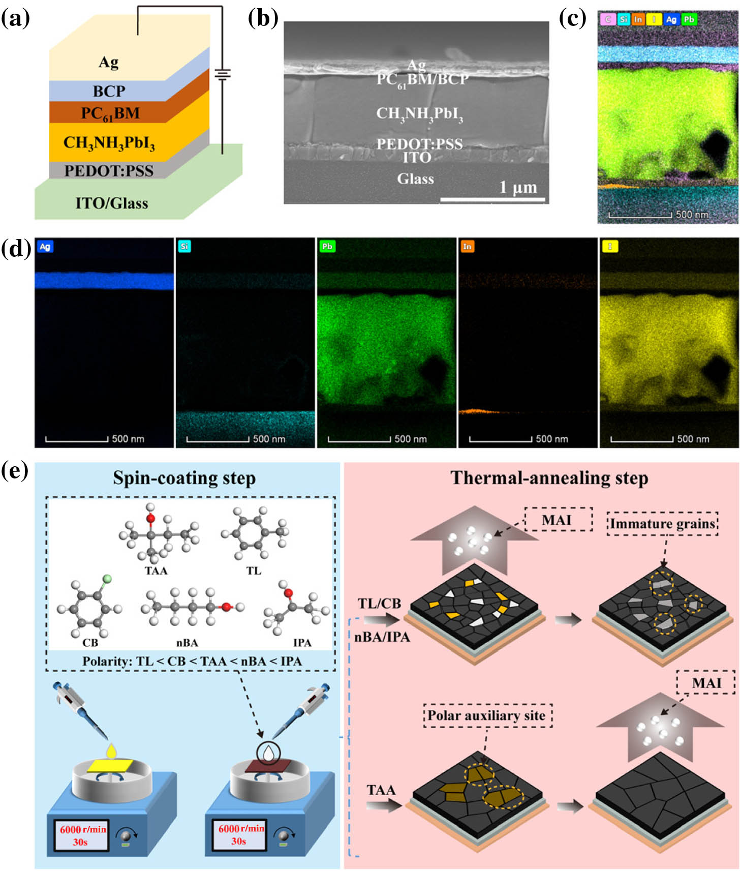
    Fig. 1. (a) Device architecture of PDs. (b) Cross-sectional SEM image of each layer in the device with a structure of (a). (c), (d) Cross-sectional EDS mapping images of different elements for each layer of the device in (a). (e) Schematic processing scheme of the antisolvent-assisted perovskite deposition process; the dashed parts are the chemical structures of antisolvents used in this work (TAA, TL, CB, nBA, and IPA).
    (a) Photograph of TAA-PSK film on ITO glass before annealing. (b) FTIR spectra of TAA-PSK films with and without annealing. (c) Photographs of different antisolvents processed films after annealing.
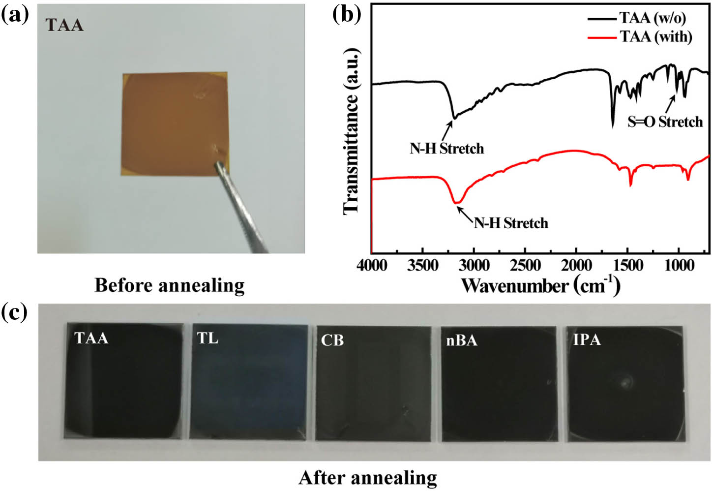
    Fig. 2. (a) Photograph of TAA-PSK film on ITO glass before annealing. (b) FTIR spectra of TAA-PSK films with and without annealing. (c) Photographs of different antisolvents processed films after annealing.
    Energy band and charge transfer diagram of PDs.
    Fig. 3. Energy band and charge transfer diagram of PDs.
    Optical properties of different antisolvent-processed films. (a) Absorption spectra. (b) XRD patterns. (c) Steady-state PL spectra; inset plots the corresponding emission peak position. (d) TRPL spectra; inset plots the values of τ1 and τ2.
    Fig. 4. Optical properties of different antisolvent-processed films. (a) Absorption spectra. (b) XRD patterns. (c) Steady-state PL spectra; inset plots the corresponding emission peak position. (d) TRPL spectra; inset plots the values of τ1 and τ2.
    Morphologies of different antisolvents processed perovskite films. (a)–(e) Top-view SEM images; the scale bar is 1 μm. (f)–(j) AFM images; the scanned area is 5 μm×5 μm, and the scale bar is 1 μm. (k)–(o) Top-view SEM images; the scale bar is 5 μm.
    Fig. 5. Morphologies of different antisolvents processed perovskite films. (a)–(e) Top-view SEM images; the scale bar is 1 μm. (f)–(j) AFM images; the scanned area is 5  μm×5  μm, and the scale bar is 1 μm. (k)–(o) Top-view SEM images; the scale bar is 5 μm.
    Grain-size distribution histograms of films based on (a) TAA-PSK, (b) TL-PSK, (c) CB-PSK, (d) nBA-PSK, and (e) IPA-PSK measured by SEM images with the scale bar of 1 μm.
    Fig. 6. Grain-size distribution histograms of films based on (a) TAA-PSK, (b) TL-PSK, (c) CB-PSK, (d) nBA-PSK, and (e) IPA-PSK measured by SEM images with the scale bar of 1 μm.
    Electrical properties of PDs. (a) I-V characteristics of the PDs processed by different antisolvents in dark condition and the illumination of 532 nm laser with a power density of 6.37 mW/cm2. (b) I-V characteristics of the TAA-PD under the illumination of 532 nm laser with different power densities. (c) Dependences of photoresponsivity of the PDs processed by different antisolvents on the incident power density at 532 nm; VBias=−2 V. (d) Dependences of detectivity of the PDs processed by different antisolvents on the incident power density at 532 nm; VBias=−2 V. (e) Dependences of EQE of the PDs processed by different antisolvents on the incident power density at 532 nm; VBias=−2 V. (f) Dependences of photocurrent of the PDs processed by different antisolvents on the incident power density at 532 nm; VBias=0 V. The linear goodness values of the fitted curves are in brackets.
    Fig. 7. Electrical properties of PDs. (a) I-V characteristics of the PDs processed by different antisolvents in dark condition and the illumination of 532 nm laser with a power density of 6.37  mW/cm2. (b) I-V characteristics of the TAA-PD under the illumination of 532 nm laser with different power densities. (c) Dependences of photoresponsivity of the PDs processed by different antisolvents on the incident power density at 532 nm; VBias=2  V. (d) Dependences of detectivity of the PDs processed by different antisolvents on the incident power density at 532 nm; VBias=2  V. (e) Dependences of EQE of the PDs processed by different antisolvents on the incident power density at 532 nm; VBias=2  V. (f) Dependences of photocurrent of the PDs processed by different antisolvents on the incident power density at 532 nm; VBias=0  V. The linear goodness values of the fitted curves are in brackets.
    Photoswitching properties of the PDs. (a) Photoswitching characteristics of the TAA-PD measured alternately in dark and under 532 nm laser illumination (1.27 mW/cm2, VBias=0 V). (b) The switching time of the TAA-PD during one ON/OFF illumination switching cycle. (c) Photocurrent stability measurement of TAA-PD for 1000 continuous switching cycles. Photoswitching characteristics of the TAA-PD under (d) 532 nm, (e) 405 nm, and (f) 808 nm laser illumination with different power densities. (g) Photoswitching characteristics of the PDs processed by different antisolvents measured alternately in dark and under 532 nm laser illumination (1.27 mW/cm2, VBias=0 V). (h) Photoswitching characteristics of the PDs processed by different antisolvents measured alternately in dark and under 405, 532, and 808 nm laser illumination (1.27 mW/cm2, VBias=0 V), respectively. (i) Photocurrent distribution of the PDs processed by different antisolvents measured alternately in dark and under 405, 532, and 808 nm laser illumination (1.27 mW/cm2, VBias=0 V), respectively. (j) Test schematic diagram of response time.
    Fig. 8. Photoswitching properties of the PDs. (a) Photoswitching characteristics of the TAA-PD measured alternately in dark and under 532 nm laser illumination (1.27  mW/cm2, VBias=0  V). (b) The switching time of the TAA-PD during one ON/OFF illumination switching cycle. (c) Photocurrent stability measurement of TAA-PD for 1000 continuous switching cycles. Photoswitching characteristics of the TAA-PD under (d) 532 nm, (e) 405 nm, and (f) 808 nm laser illumination with different power densities. (g) Photoswitching characteristics of the PDs processed by different antisolvents measured alternately in dark and under 532 nm laser illumination (1.27  mW/cm2, VBias=0  V). (h) Photoswitching characteristics of the PDs processed by different antisolvents measured alternately in dark and under 405, 532, and 808 nm laser illumination (1.27  mW/cm2, VBias=0  V), respectively. (i) Photocurrent distribution of the PDs processed by different antisolvents measured alternately in dark and under 405, 532, and 808 nm laser illumination (1.27  mW/cm2, VBias=0  V), respectively. (j) Test schematic diagram of response time.
    Electrical and photoswitching properties of TL-PD. (a) I-V characteristics under the illumination of 532 nm laser with different power densities. (b) Photoswitching characteristics measured alternately in dark and under 532 nm laser illumination (1.27 mW/cm2, VBias=0 V). (c) Switching time of the TL-PD during one ON/OFF illumination switching cycle. Photoswitching characteristics under (d) 532 nm, (e) 405 nm, and (f) 808 nm laser illumination with different power densities.
    Fig. 9. Electrical and photoswitching properties of TL-PD. (a) I-V characteristics under the illumination of 532 nm laser with different power densities. (b) Photoswitching characteristics measured alternately in dark and under 532 nm laser illumination (1.27  mW/cm2, VBias=0  V). (c) Switching time of the TL-PD during one ON/OFF illumination switching cycle. Photoswitching characteristics under (d) 532 nm, (e) 405 nm, and (f) 808 nm laser illumination with different power densities.
    Electrical and photoswitching properties of CB-PD. (a) I-V characteristics under the illumination of 532 nm laser with different power densities. (b) Photoswitching characteristics measured alternately in dark and under 532 nm laser illumination (1.27 mW/cm2, VBias=0 V). (c) Switching time of the CB-PD during one ON/OFF illumination switching cycle. Photoswitching characteristics under (d) 532 nm, (e) 405 nm, and (f) 808 nm laser illumination with different power densities.
    Fig. 10. Electrical and photoswitching properties of CB-PD. (a) I-V characteristics under the illumination of 532 nm laser with different power densities. (b) Photoswitching characteristics measured alternately in dark and under 532 nm laser illumination (1.27  mW/cm2, VBias=0  V). (c) Switching time of the CB-PD during one ON/OFF illumination switching cycle. Photoswitching characteristics under (d) 532 nm, (e) 405 nm, and (f) 808 nm laser illumination with different power densities.
    Electrical and photoswitching properties of nBA-PD. (a) I-V characteristics under the illumination of 532 nm laser with different power densities. (b) Photoswitching characteristics measured alternately in dark and under 532 nm laser illumination (1.27 mW/cm2, VBias=0 V). (c) Switching time of the nBA-PD during one ON/OFF illumination switching cycle. Photoswitching characteristics under (d) 532 nm, (e) 405 nm, and (f) 808 nm laser illumination with different power densities.
    Fig. 11. Electrical and photoswitching properties of nBA-PD. (a) I-V characteristics under the illumination of 532 nm laser with different power densities. (b) Photoswitching characteristics measured alternately in dark and under 532 nm laser illumination (1.27  mW/cm2, VBias=0  V). (c) Switching time of the nBA-PD during one ON/OFF illumination switching cycle. Photoswitching characteristics under (d) 532 nm, (e) 405 nm, and (f) 808 nm laser illumination with different power densities.
    Electrical and photoswitching properties of IPA-PD. (a) I-V characteristics under the illumination of 532 nm laser with different power densities. (b) Photoswitching characteristics measured alternately in dark and under 532 nm laser illumination (1.27 mW/cm2, VBias=0 V). (c) Switching time of the IPA-PD during one ON/OFF illumination switching cycle. Photoswitching characteristics under (d) 532 nm, (e) 405 nm, and (f) 808 nm laser illumination with different power densities.
    Fig. 12. Electrical and photoswitching properties of IPA-PD. (a) I-V characteristics under the illumination of 532 nm laser with different power densities. (b) Photoswitching characteristics measured alternately in dark and under 532 nm laser illumination (1.27  mW/cm2, VBias=0  V). (c) Switching time of the IPA-PD during one ON/OFF illumination switching cycle. Photoswitching characteristics under (d) 532 nm, (e) 405 nm, and (f) 808 nm laser illumination with different power densities.
    Samplesτ1 (ns)A1 (%)τ2 (ns)A2 (%)
    TAA-PSK20.6827.6880.8272.32
    TL-PSK2.4337.9657.0962.04
    CB-PSK14.6539.4878.9260.52
    nBA-PSK2.6024.2249.4275.78
    IPA-PSK2.4020.3449.1979.66
    Table 1. Summary of the Performance of PDs
    Device StructureWavelength(nm)Responsivity(A/W)Detectivity(Jones)Response Time Rise/Fall TimeReferences
    ITO/PEDOT:PSS/CH3NH3PbI3/PCBM/BCP/Al5000.879.1×1011-/26.1  μs[42]
    ITO/TiO2/PCBM/CH3NH3PbI3/P3HT/MoO3/Ag5000.344.8×1012[43]
    FTO/TiO2/AlO3/PCBM/CH3NH3PbI3/Spiro/Au/Ag6000.410121.2 μs/3.2 μs[44]
    ITO/PEDOT:PSS/CH3NH3PbI3/PCBM/Al6700.3144 μs/3 μs[45]
    ITO/PEDOT:PSS/CH3NH3PbI3/PCBM/AZO/Al7000.3[46]
    FTO/TiO2/CH3NH3PbI3/Spiro/Au6600.186.3×1010[47]
    ITO/PEDOT:PSS/CH3NH3PbI3/PCBM/BCP/Ag(TAA-PSK)5321.561.47×1012204 ns/358 nsThis work
    ITO/PEDOT:PSS/CH3NH3PbI3/PCBM/BCP/Ag(TL-PSK)5320.461.78×1011320 ns/720 nsThis work
    ITO/PEDOT:PSS/CH3NH3PbI3/PCBM/BCP/Ag(CB-PSK)5320.612.58×1011304 ns/656 nsThis work
    ITO/PEDOT:PSS/CH3NH3PbI3/PCBM/BCP/Ag(nBA-PSK)5320.351.56×1011348 ns/768 nsThis work
    ITO/PEDOT:PSS/CH3NH3PbI3/PCBM/BCP/Ag(IPA-PSK)5320.301.48×1011364 ns/744 nsThis work
    Table 2. Performance Parameters of PPDs with Vertical Structure
    Tengteng Li, Qingyan Li, Xin Tang, Zhiliang Chen, Yifan Li, Hongliang Zhao, Silei Wang, Xin Ding, Yating Zhang, Jianquan Yao. Environment-friendly antisolvent tert-amyl alcohol modified hybrid perovskite photodetector with high responsivity[J]. Photonics Research, 2021, 9(5): 781
    Download Citation