• Infrared and Laser Engineering
  • Vol. 52, Issue 6, 20230269 (2023)
Jiaqi Wen1、2, Jintian Bian1、2, Xin Li1、2, Hui Kong1、2, Lei Guo3, and Guorui Lv1、2
Author Affiliations
  • 1State Key Laboratory of Pulsed Power Laser Technology, Electronic Countermeasure Institute, National University of Defense Technology, Hefei 230037, China
  • 2Anhui Laboratory of Advanced Laser Technology, Electronic Countermeasure Institute, National University of Defense Technology, Hefei 230037, China
  • 3School of Mechanics and Optoelectronic Physics, Anhui University of Science and Technology, Huainan 232001, China
  • show less
    DOI: 10.3788/IRLA20230269 Cite this Article
    Jiaqi Wen, Jintian Bian, Xin Li, Hui Kong, Lei Guo, Guorui Lv. Research progress of laser dazzle and damage CMOS image sensor (invited)[J]. Infrared and Laser Engineering, 2023, 52(6): 20230269 Copy Citation Text show less
    Effect of pulsed laser parameters on damage
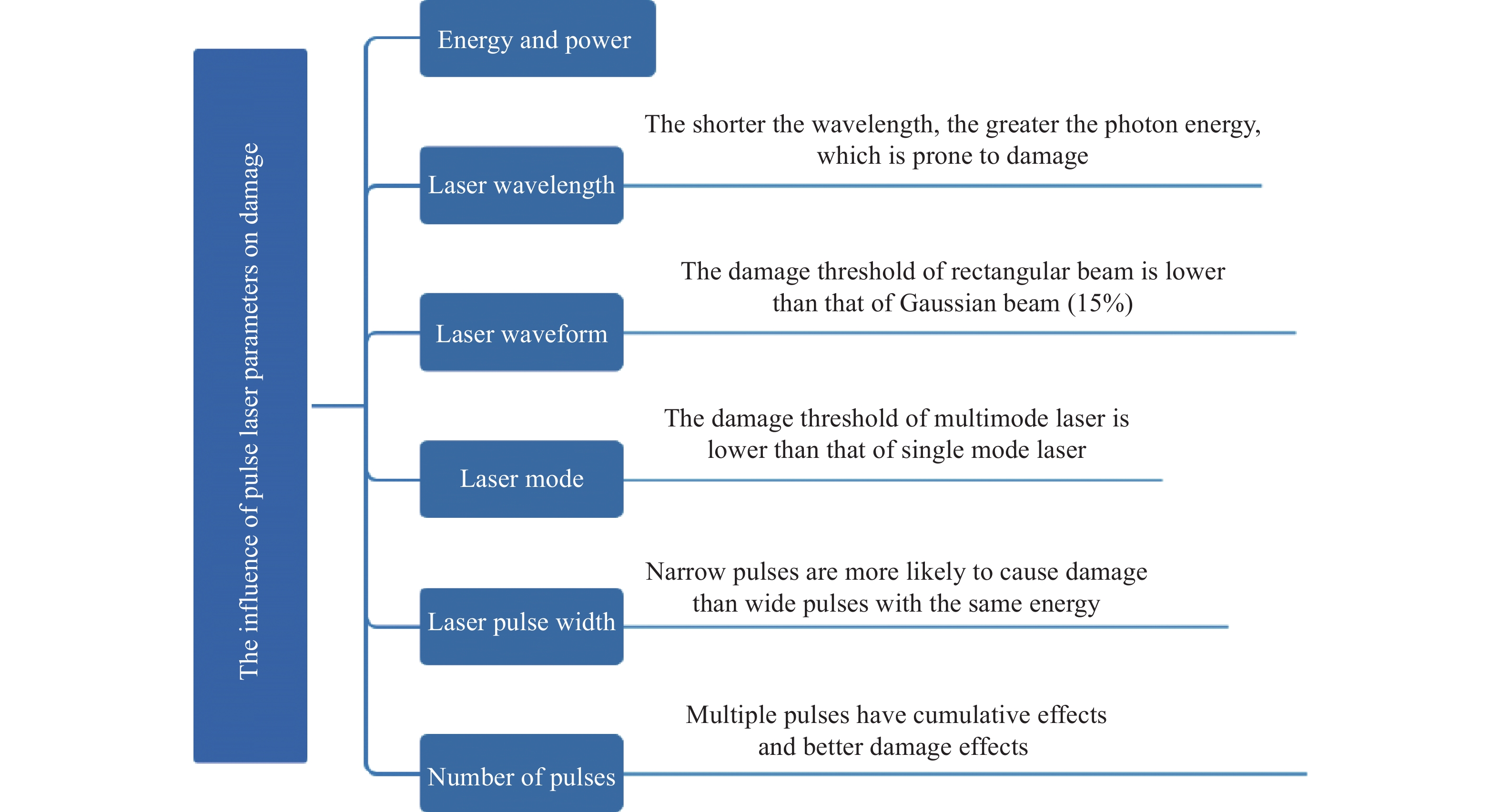
    Fig. 1. Effect of pulsed laser parameters on damage
    (a) Pixel structures of passive pixel CMOS and (b) active pixel CMOS[13]
    Fig. 2. (a) Pixel structures of passive pixel CMOS and (b) active pixel CMOS[13]
    DTI between CMOS pixels[15]
    Fig. 3. DTI between CMOS pixels[15]
    Schematic of the structure of the Front Side Illuminated CMOS image sensor[5]
    Fig. 4. Schematic of the structure of the Front Side Illuminated CMOS image sensor[5]
    Comparison of pixel structures between the FSI-CMOS and BSI-CMOS. (a) Front lighting structure; (b) Back lighting structure
    Fig. 5. Comparison of pixel structures between the FSI-CMOS and BSI-CMOS. (a) Front lighting structure; (b) Back lighting structure
    Correlated double sampling working process of CMOS pixels[16]
    Fig. 6. Correlated double sampling working process of CMOS pixels[16]
    Curve of interference area with incident laser energy density[4]
    Fig. 7. Curve of interference area with incident laser energy density[4]
    Comparison of irreversible damage to CMOS and CCD by nanosecond laser[24]
    Fig. 8. Comparison of irreversible damage to CMOS and CCD by nanosecond laser[24]
    Comparison of morphology of CMOS surface damage induced by different lasers[24]. (a) Morphology of picosecond laser damage; (b) Morphology of femtosecond laser damage
    Fig. 9. Comparison of morphology of CMOS surface damage induced by different lasers[24]. (a) Morphology of picosecond laser damage; (b) Morphology of femtosecond laser damage
    Comparison of damage to CCD, FSI-CMOS and BSI-CMOS[11]
    Fig. 10. Comparison of damage to CCD, FSI-CMOS and BSI-CMOS[11]
    Laser sourceCMOS modelSaturationOver saturationCrosstalkFull screen saturation
    1.06 mm, 64 kHz, 10 nsSONY IMX035LQZ-C35.8 W/cm2--4.3×103 W/cm2
    1.06 mm, 10 Hz, 5 nsDH HV1300FM7.70×10−2 J/cm2---
    1.06 mm, 10 Hz, 5 ns (vacuum)DH HV1300FM7.70×10- 2 J/cm2---
    532 nm CWMicron MT9V0224.32×10−4 W/cm28.7×102 W/cm2--
    1064 nm CWMicron MT9V0225.87×10−3 W/cm26.0×102 W/cm22.0×103 W/cm22.0×103 W/cm2
    632 nm CWDH HV-U 1×10⁻¹ mW ---
    632 nm CWMicron MT9V0324.2×10−5 W/cm24.1 W/cm2-11.6-24.3 W/cm2
    1031 nm, 226.5 ps, 9.6 MHzMicron MT9V034 -2.3 mW630 mW-
    1031 nm, 226.5 ps, 2.4 MHzMicron MT9V034 -1.3 mW28.5 mW-
    1064 nm, 5 Hz, 10 nsMicron MT9V032 ---0.76 mJ/cm
    Table 1. Comparison of laser interference thresholds for CMOS image sensors
    Laser sourceCMOS modelTest methodPoint damageBlack line damageCross damage
    1064 nm, 10 Hz, 5 nsDH HV1300FM1-on-10.5 J/cm2-626 J/cm2
    1064 nm, 10 Hz, 5 ns (vacuum)DH HV1300FM1-on-10.5 J/cm2-273 J/cm2
    1064 nm, 60 nsMicron MT9V022l-on-10.38 J/cm20.64 J/cm21.0 J/cm2
    1064 nm, 25 psMicron MT9V022l-on-119.1 mJ/cm267.8 mJ/cm2130.1 mJ/cm2
    800 nm, 100 fsMicron MT9V022l-on-14.1 mJ/cm2--
    1.06 mm, 10 ns double-pulses, interval 80 ns Micron MT9V0221-on-10.29 J/cm2(double) --
    1-on-10.67 J/cm2 (single)
    1031 nm, 226.5 ps, 9.6 MHzMicron MT9 V034S-on-1-1.06 W2.5 W
    1031 nm, 226.5 ps, 2.4 MHzMicron MT9V034S-on-1-720 mW800 mW
    532 nm, CWDCC1645CS-on-1150 kW/cm21400 kW/cm2>4000 kW/cm2 (destroyed)
    532 nm, CWDCC1545MS-on-1800 kW/cm21100 kW/cm2>4000 kW/cm2 (destroyed)
    532 nm, 10 nsMT9V024l-on-10.035 J/cm238.6 J/cm2-
    526.5 nm, 8.2 psMT9V024l-on-10.01 J/cm218 J/cm2-
    Table 2. Comparison of laser damage thresholds for CMOS image sensors
    Jiaqi Wen, Jintian Bian, Xin Li, Hui Kong, Lei Guo, Guorui Lv. Research progress of laser dazzle and damage CMOS image sensor (invited)[J]. Infrared and Laser Engineering, 2023, 52(6): 20230269
    Download Citation